How
to design an
enclosure using the Laser cutter in the Engineering College maker space.
Jonathan
Valvano, EE445L,
University of Texas at Austin
Background
steps
1) Get trained on the Full Spectrum Hobby and Pro Laser Cutters, http://makerspace.engr.utexas.edu/
2) Download and install the Retina Engrave Software on your laptop from
http://www.fullspectrumengineering.com/RetinaEngraveProtected.html
3) Download and install PCB artist from www.4pcb.com/free-pcb-layout-software
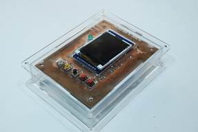
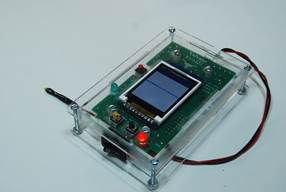
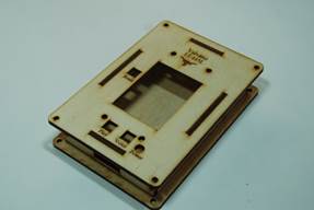
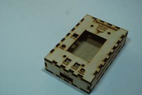
Figure
1.
Example boxes (Lab3Box, Lab9Box, WoodBox
and WoodBox2).
Planning
steps
0) Choose
whether you wish to build the box out of
acrylic or wood, and obtain the raw material so you can double check
its
thickness. Download the box starter file specific for that material,
and which
best matches your needs. The sizes in this list are the inside
dimensions of
the enclosure. Download
Lab3Box.pcb
is a 4.08 by 3.04 by 1.04 inch box, 80 mil acrylic, 8
by 8 inch raw material.
Lab9Box.pcb is a 3.92 by 2.4 by 0.72 inch box, 80 mil acrylic, 8 by 8 inch raw material.
CirqoidBox.pcb is a 4.10 by 3.10 by 1.00 inch box, 100 mil acrylic, 8 by 8 inch raw material.
WoodBox.pcb
is a 4.00 by 2.5 by 0.75 inch box, 125 mil wood, 6.5
by 9.5 inch raw material.
WoodBox2.pcb is a 4.00 by 2.5 by 0.75 inch box, 125 mil wood, 6 by 8.5 inch raw material.
Lab3Box93.pcb
is a 4.65 by 2.418 by 1.488 inch box, 93 mil acrylic, 9.3
by 8 inch raw material
Lab3Box93square.pcb
is a 4.65 by 2.418 by 1.488 inch box, 93 mil acrylic, 9.3
by 8 inch raw material
Lab10Box93.pcb
is a 5.58 by 2.976 by 0.93 inch box, 93 mil acrylic, 10.4
by 8 inch raw material
For
the 80 mil acrylic all slots are down-sized to 70
mil
so the pieces will fit snugly. For
the 93 mil acrylic all slots are down-sized to 84
mil
so the pieces will fit snugly.
For the 100 mil acrylic all slots are
down-sized
to 90
mil so the pieces will fit
snugly. For the 125
mil wood all slots are sized to 115 mil.
The board
outline layer can be used to determine the amount of raw material
needed.
1)
You can design your box with the same application with which you
designed your
PCB. I used PCB
Artist for these
examples. Open the appropriate starter file and print all layers of the
existing starter file at 100%. Find some cardboard that has a thickness
approximately equal to your final material. Glue the paper printout to
the
cardboard, and cut out the pieces. This step is important for you to
visualize
how the six parts designed in two dimensions will fit together to make
a 3-D
object. It is important to keep straight which side of each piece is
up/down,
left/right, and inside/outside. The paper printout exists on the 6
outside
faces of the box. Save the PCB file with a different name. Figure 2
shows the
top side of Lab9Box.pcb
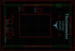
Figure
2.
Design in PCB Artist.
2)
Think about the mapping between PCB layers and the build process. I set
PCB
Artist to view only the layers used in the design: document, top
copper, top
silk, bottom silk, and board outline. I use the document
layer to define parameters not translated to either cuts
(vector) or etching (raster). Notice I added labels in the document
layer to
show the left/right, front/back, and top/bottom orientation. I use the top copper
layer to define all cuts. In
particular, I will cut holes in the sides of the box for items like
LEDs and
switches. The top copper layer also defines where in the box I wish
drill
holes. I use the top
silk layer to
define labels that will be etched on the pieces in raster mode. I use
the bottom silk
layer to define the other
piece situated in an orthogonal dimension.
In PCB Artist the etching
occurs on the outside layer, and the inside
layer will not be etched. I
use the board
outline layer to define the size
of the raw material from which the 6 pieces will be cut. Execute Settings->Grids
and set the Step
Size to match your material
thickness, and set the Snap
Mode to Grid.
The
following figure shows the settings for
the 80 mil acrylic on the left, and the 125 mil wood
on the right.
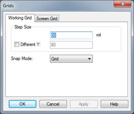
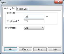
Figure 3.
Settings->Grids for 80 mil acrylic
and
125 mil wood.
3)
If you need to change the material thickness, you should make this
change
first. You should move all edges of each piece so it snaps to the Grid,
which
is the material thickness. Obviously, make sure the inside of the box
has room
to fit the PCB and other components you wish to house.
4)
Next, adjust the size of the box as needed. It is really helpful to
leave the
snap to Grid at the same setting so all box dimensions are multiples of
the
material thickness. Top and bottom pieces should be the same size, left
and
right should be the same size. Front and back should be the same.
Adjust the
slots so they all fit together. One trick I use to make sure it fits is
1) save
the PCB, 2) move/rotate pieces overtop each other to see all the slots
will fit,
3) revert to the saved version. This is where the documentation helps
to know
which edges should line up.
5)
Next, open the PCB file that contains your actual PCB. In the box PCB,
change
the grid snap to value convenient for the actual PCB. Select components
like
the PCB mounting holes, LEDs, switches, display, and PCB board outline.
Select
all components that will physically interact with the box. Copy these
components and paste them into the box PCB over the top (or bottom)
side of the
box. Move all these components together. Remember the box PCB shows the
outside
view of the box top, so you may have to flip the actual PCB depending
on how
you plan to mount the actual PCB into the box. The white in Figure 4
shows the
PCB pasted over the top side of the box. The pasted actual PCB
components have
been flipped and rotated by 180 so the bottom copper layer of the
actual PCB
physically touches the inside of the top of the box.
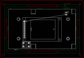
Figure
4.
Components of the actual PCB
pasted over the top side of the box
The
next step is to draw top copper rectangles for switch and display, and
to draw
circles for the LED and mounting screws. Recall the top copper layer
will be
cut by the laser. Next, add top silk to label the six sides of the box
as
desired. Recall the top silk will be etched on the material. You can
add holes
and rectangles on the other sides for off board switches and
connectors. It is
important to remove or change layer to document all top copper that was
pasted
in from the actual PCB. Figure 5 shows the final edit. Remember, first
we will
etch the top silk (raster) and then cut with the top copper layer. It
is
helpful to observe the design with just top copper and top silk. Zoom
way in to
make sure there are not two or more copies of top copper objects.
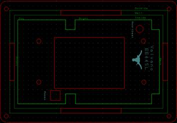
Figure
5.
The top side of the box with
cutouts for display,
switch and LED.
6)
Measure twice
and cut once. You
should not skip this step. Print out both your PCB and your box. Glue
the
pieces to cardboard and cut out the sides. Verify the labels are on the
outside
of the box and the slots, grooves and tabs will fit together.
7)
There are eight slots, four on the top and four on the bottom. Once you
are
sure you do not wish to change the size of the box, we will shrink the
size of
the eight slots so the pieces will fit snuggly. For the 80-mil acrylic,
we will
reduce the width of the slot from 80 to 70 mil.
For
the 93-mil acrylic,
we will
reduce the width of the slot from 93 to 84 mil.
For
the 100-mil acrylic, we will reduce the width of the slot from 100 to 90 mil.
For the 125-mil wood, we will reduce the width of
the slot from 125 to
115 mil. We wish to move both
sides of each slot by
5 mil, so we set the Grid to
5
mil, Figure 6. Figure 7A shows the slot before and Figure 7B shows the
slot
after reduction. This step accounts for the amount of material that
will be
removed by the laser during cutting.
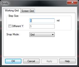
Figure
6.
Settings->Grids for ½ the
desired shrinkage. For 93-mil acrylic I set the grid to 3mil and moved
one side 6 mils and the other side I moved three mil.

Figure
7A.
A slot is originally 1680 by 80 mil.

Figure
7B.
We shrink the slot to 1680 by 70 mil.
Notice both lines are moved towards each other.
8) To prepare for cutting make a pdf print of just the top copper, and a second pdf print of just the top silk. Make both prints 100 %, all black. The portrait/landscape orientation should be the same. The laser cutters have more horizontal dimension than vertical dimension. Print the pdf at 100% and cutout the copper pieces to verify orientations are correct.
Cutting
steps
1)
Follow all safety and procedural steps as instructed by the Makerspace.
2)
First etch the labels by printing the top silk
3)
Second, cut the pieces by printing the top copper layer.
If
you have any comments or corrections please contact me at
valvano@mail.utexas.edu