(Please refer to the figure for problem 3.7 on page 84 of the book) The circuit has a major flaw. Can you identify it? Hint: Evaluate the circuit for all sets of inputs.
A B C |
NOT(NOT(A) AND NOT(B) AND NOT(C)) |
|---|---|
0 0 0 |
|
0 0 1 |
|
0 1 0 |
|
0 1 1 |
|
1 0 0 |
|
1 0 1 |
|
1 1 0 |
|
1 1 1 |
|
- Draw a transistor-level diagram for a three-input AND gate and a three-input OR gate. Do this by extending the designs from Figures 3.6a and 3.7a. (Figures can be found in the book on pages 56 & 57 respectively).
- Replace the transistors in your diagrams from part (a)
with either a wire or no wire to reflect the circuit’s operation when
the following inputs are applied:
- A = 1, B = 0, C = 0
- A = 0, B = 0, C = 0
- A = 1, B = 1, C = 1
- How many output lines will a five-input decoder have?
- How many output lines will an eight-input decoder have?
- How many output lines will an N-input decoder have? (N can be any number)
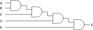
Figure 1
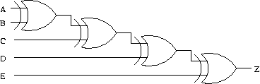
Figure 2
- Complete a truth table for the gate-level logic circuit shown in Figure 2 above.
- What do you notice about the input combinations that give an output value of 1? What do you notice about the input combinations that give an output value of 0?
Given the following truth table, generate the gate-level logic circuit, using the implementation algorithm referred to in Section 3.3.4.
A B C |
Z |
|---|---|
0 0 0 |
1 |
0 0 1 |
0 |
0 1 0 |
0 |
0 1 1 |
1 |
1 0 0 |
0 |
1 0 1 |
1 |
1 1 0 |
1 |
1 1 1 |
0 |
Implement the following functions using AND, OR, and NOT logic gates. The inputs are A, B, and the output is F.
- F has the value 1 only if A has the value 0 and B has the value 1.
- F has the value 1 only if A has the value 1 and B has the value 0.
- Use your answers from (a) and (b) to implement a 1-bit adder. The truth table for the 1-bit adder is given below.
- Is it possible to create a 4-bit adder (a circuit that will correctly add two 4-bit quantities) using only four copies of the logic diagram from (c)? If not, what information is missing? Hint: When A = 1 and B = 1, a sum of 0 is produced. What information is not dropped?
A B |
Sum |
|---|---|
0 0 |
0 |
0 1 |
1 |
1 0 |
1 |
1 1 |
0 |
Logic circuit 1 in Figure 3.36 (page 87 of the book) has inputs A, B, C. Logic circuit 2 in Figure 3.37 (page 87 of the book) has inputs A and B. Both logic circuits have an output D. There is a fundamental difference between the behavioral characteristics of these two circuits. What is it? Hint: What happens when the voltage at input A goes from 0 to 1 in both circuits?
Implement a 4-to-1 mux using only 2-to-1 muxes making sure to properly connect all of the terminals. Remember that you will have 4 inputs, 2 control signals, and 1 output. Write out the truth table for this circuit.
- Figure 3.39 (page 89 of the book) shows a logic circuit that appears in many of today’s processors. Each of the boxes is a full-adder circuit. What does the value on the wire X do? That is, what is the difference in the output of this circuit if X = 0 versus if X = 1?
- Construct a logic diagram that implements an adder/subtracter. That is, the logic circuit will compute A + B or A – B depending on the value of X. Hint: Use the logic diagram of Figure 3.39 as a building block.
Recall that the adder was built with individual "slices" that produced a sum bit and carryout bit based on the two operand bits A and B and the carryin bit. We called such an element a full-adder. Suppose we have a 3-to-8 decoder and two six-input OR gates, as shown in Figure 3 below. Can we connect them so that we have a full-adder? If so, please do. (Hint: If an input to an OR gate is not needed, we can simply put an input 0 on it and it will have no effect on anything. For example, see the figure below.)
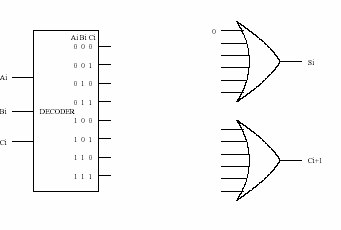
Figure 3