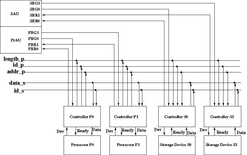
We show below a synchronous split transaction bus system employing centralized arbitration. There are two processors (P0 and P1) and two storage devices (S0 and S1). For the sake of simplicity, we assume that processors will only read data from the the storage devices.
Arbitration
There are two arbitration units, Processor Arbitration Unit(PrAU) and Storage Device Arbitration Unit(SAU). PrAU arbitrates the addr_p bus across P0 and P1. SAU arbitrates the data bus across S0 and S1. This allows one processor to request a transfer while the other processor is receiving data. P0 has higher priority than P1 and S0 has higher priority than S1.
Data Transfer
The following is how a transfer between Processor i (Pi) and Storage Device j (Sj) proceeds:
- When Pi needs data from Sj, it asserts the Bus Request signal (PBRi). Upon receiving the Bus Grant signal (PBGi) from the PrAU, the controller asserts the starting address on addr_p, the Vaddr (valid address signal, not shown in the figure), number of elements to be transfered on signal length_p (Count), and its Id (i in this case) on id_p signal. Pi now waits for data from Sj.
- When Sj sees an address that lies in its address range with Vaddr asserted, it latches the address, length, and Id and starts processing the request.
- When Sj is ready to return a data element, it asserts SBRj and upon receiving the Grant signal (SBGj), it asserts data on data_s, the Id of the processor that requested the data on id_s and the Vid (valid id signal, where Vid = SBG0 OR SBG1, not shown in the figure). It also decrements its Count of the remaining elements. The SBGj signal grants the bus to Sj for a single cycle.
- When Pi sees its Id on id_s with Vid signal asserted, it latches the data element and decrements its Count.
- Pi and Sj cycle through steps 3 and 4 until Count reaches 0.
The device and controller synchronize using the Dev and Ready signals. When a transfer needs to be carried out the Dev signal is asserted. The availability of valid data is indicated by asserting the Ready signal.
Note: for the sake of simplicity, assume each processor can have only one pending transfer.
Each storage device controller can buffer up to two requests since each processor could have one pending transfer from a given storage.
-
Construct the state machine for the processor controller Pi. Show relevant inputs and outputs on all arcs. (Remember that the controller keeps track of the number of data transfers completed in a Count
signalregister.) -
Assume that the controller consists of a state machine and a two-entry buffer: (Corrected: 04/12/2007 – changed directions of Dev and Ready signals)
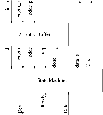
Whenever the storage controller is requested on the bus, the buffer stores the id_p, length_p, and addr_p bus signals. The req output of the buffer indicates that at least one request is awaiting service in the buffer. The id, length, and addr signals are the buffered bus signals of the oldest buffered bus request. The done input tells the buffer to clear the oldest buffered request.
Draw the state diagram for the state machine in the figure above. Show relevant inputs and outputs on all arcs.
We added a small cache to the LC-3b processor. The data store size is 64 bytes and the cache line size is 16 bytes. When a given program is executed, the processor reads data from the following sequence of hex addresses:
x3210, x3212, x3318, x3394, x3214, x3040, x3218, x3394, x3310, x3390
This pattern is repeated three times.
-
Show the contents of the cache at the end of each pass throughout this loop if a direct-mapped cache is used. Compute the hit rate for this example. Assume that the cache is initially empty.
-
Repeat part (a) for a two way set-associative cache that uses the LRU-replacement algorithm.
-
Repeat part (a) for a fully-associative cache that uses the LRU replacement algorithm.
Given the following code:
MUL R3, R1, R2
ADD R5, R4, R3
ADD R6, R4, R1
MUL R7, R8, R9
ADD R4, R3, R7
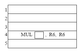
MUL R10, R5, R6Note: Each instruction is specified with the destination register first.
Calculate the number of cycles it takes to execute the given code on the following models:
- A non-pipelined machine.
- A pipelined machine with scoreboarding and five adders and five multipliers.
- A pipelined machine with scoreboarding and one adder and one multiplier.
Note: For all machine models, use the basic instruction cycle as follows:
- Fetch (one clock cycle)
- Decode (one clock cycle)
- Execute (MUL takes 6, ADD takes 4 clock cycles). The multiplier and the adder are not pipelined.
- Write-back (one clock cycle)
Do not forget to list any assumptions you make about the pipeline structure (e.g., data forwarding between pipeline stages).
Suppose we have the following loop executing on a pipelined LC-3b machine.
DOIT     STW   R1, R6, #0
         ADD   R6, R6, #1 #2
         AND   R3, R1, R2
         BRz   EVEN
         ADD   R1, R1, #3
         ADD   R5, R5, #-1
         BRp   DOIT
EVEN     ADD   R1, R1, #1
         ADD   R7, R7, #-1
         BRp   DOIT
Assume that before the loop starts, the registers have the following decimal values stored in them:
| Register | Value |
|---|---|
| R0 | 0 |
| R1 | 0 |
| R2 | 1 |
| R3 | 0 |
| R4 | 0 |
| R5 | 5 |
| R6 | 4000 |
| R7 | 5 |
The fetch stage takes one cycle, the decode stage also takes one cycle, the execute stage takes a variable number of cycles depending on the type of instruction (see below), and the store stage takes one cycle.
All execution units (including the load/store unit) are fully pipelined and the following instructions that use these units take the indicated number of cycles:
| Instruction | Number of Cycles |
|---|---|
| STW | 3 |
| ADD | 3 |
| AND | 2 |
| BR | 1 |
Data forwarding is used wherever possible. Instructions that are dependent on the previous instructions can make use of the results produced right after the previous instruction finishes the execute stage.
The target instruction after a branch can be fetched when the BR instruction is in ST stage. For example, the execution of an ADD instruction followed by a BR would look like:
ADD       F | D | E1 | E2 | E3 | ST
BR            F | D  | -  | -  | E1 | ST
TARGET                                F  | D
The pipeline implements “in-order execution.” A scoreboarding scheme is used as discussed in class.
Answer the following questions:
How many cycles does the above loop take to execute if no branch prediction is used?
How many cycles does the above loop take to execute if all branches are predicted with 100% accuracy.
How many cycles does the above loop take to execute if a static BTFN (backward taken-forward not taken) branch prediction scheme is used to predict branch directions? What is the overall branch prediction accuracy? What is the prediction accuracy for each branch?
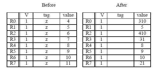
A five instruction sequence executes according to Tomasulo's
algorithm. Each instruction is of the form ADD DR,SR1,SR2 or MUL
DR,SR1,SR2. ADDs are pipelined and take 9 cycles
(F-D-E1-E2-E3-E4-E5-E6-WB). MULs are also pipelined and take 11 cycles (two
extra execute stages). The microengine must wait until a result is in
a register before it sources it (reads it as a source operand).
The register file before and after the sequence are shown below (tags for “After” are ignored).
-
Complete the five instruction sequence in program order in the space below. Note that we have helped you by giving you the opcode and two source operand addresses for instruction 4. (The program sequence is unique.)
-
In cycle 1 instruction 1 is fetched. In cycle 2, instruction 1 is decoded and instruction 2 is fetched. In cycle 3, instruction 1 starts execution, instruction 2 is decoded, and instruction 3 is fetched.
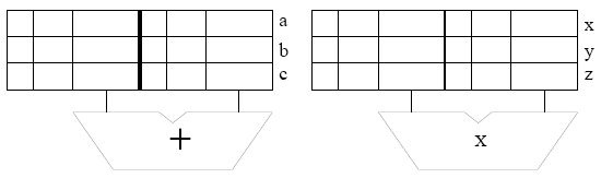
Assume the reservation stations are all initially empty. Put each instruction into the next available reservation station. For example, the first ADD goes into “a”. The first MUL goes into “x”. Instructions remain in the reservation stations until they are completed. Show the state of the reservation stations at the end of cycle 8.
Note: to make it easier for the grader, when allocating source registers to reservation stations, please always have the higher numbered register be assigned to SR2.
-
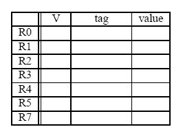
Show the state of the Register Alias Table (V, tag, Value) at the end of cycle 8.
Consider the following piece of code:
for(i = 0; i < 100; i++)
  A[i] = ((B[i] * C[i]) + D[i]) / 2;
Translate this code into assembly language using the following instructions in the ISA (note the number of cycles each instruction takes is shown with each instruction):
Opcode Operands Number of Cycles Description LEARi, X1 Ri ← address of X LDRi, Rj, Rk11 Ri ← MEM[Rj + Rk] STRi, Rj, Rk11 MEM[Rj + Rk] ← Ri MOVIRi, Imm1 Ri ← Imm MULRi, Rj, Rk6 Ri ← Rj × Rk ADDRi, Rj, Rk4 Ri ← Rj + Rk ADDRi, Rj, Imm4 Ri ← Rj + Imm RSHFARi, Rj, amount1 Ri ← RSHFA (Rj, amount) BRccX1 Branch to X based on condition codes Assume it takes one memory location to store each element of the array. Also assume that there are 8 registers (R0-R7).
How many cycles does it take to execute the program?
-
Now write Cray-like vector/assembly code to perform this operation in the shortest time possible. Assume that there are 8 vector registers and the length of each vector register is 64. Use the following instructions in the vector ISA:
Opcode Operands Number of Cycles Description LDVst, #n1 Vst ← n LDVln, #n1 Vln ← n VLDVi, X11, pipelined VSTVi, X11, pipelined VmulVi, Vj, Vk6, pipelined VaddVi, Vj, Vk4, pipelined VrshfaVi, Vj, amount1 VbrccX1 How many cycles does it take to execute the program on the following processors? Assume that memory is 16-way interleaved.
- Vector processor without chaining, 1 port to memory (1 load or store per cycle)
- Vector processor with chaining, 1 port to memory
- Vector processor with chaining, 2 read ports and 1 write port to memory
Little Computer Inc. is now planning to build a new computer that is more suited for scientific applications. LC-3b can be modified for such applications by replacing the data type Byte with Vector. The new computer will be called LmmVC-3 (Little 'mickey mouse' Vector Computer 3). Your job is to help us implement the datapath for LmmVC-3. LmmVC-3 ISA will support all the scalar operations that LC-3b currently supports except the LDB and STB will be replaced with VLD and VST respectively. Our datapath will need to support the following new instructions:
Note: VDR means “Vector Destination Register” and VSR means “Vector Source Register.”
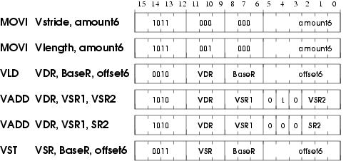
- MOVI
- If IR[11:9] = 000, MOVI moves the unsigned quantity amount6 to Vector Stride Register (Vstride). If IR[11:9] = 001, MOVI moves the unsigned quantity amount6 to Vector Length Register (Vlength). This instruction has already been implemented for you.
- VLD
- VLD loads a vector of length Vlength from memory into VDR. VLD uses the opcode previously used by LDB. The starting address of the vector is computed by adding the LSHF1(SEXT(offset6)) to BaseR. Subsequent addresses are obtained by adding LSHF1(ZEXT(Vstride)) to the address of the preceding vector element.
- VST
- VST writes the contents of VSR into memory. VST uses the opcode previously used by STB. Address calculation is done in the same way as for VLD.
- VADD
- If IR[4] is a 1, VADD adds two vector registers (VSR1 and VSR2) and stores the result in VDR. If IR[4] is a 0, VADD adds a scalar register (SR2) to every element of VSR and stores the result in VDR.
VLD, VST, and VADD do not modify the content of Vstride and Vlength registers.
The following five hardware structures have been added to LC-3b in order to implement LmmVC-3.
- Vector Register File with eight 63-element Vector registers
- Vector Length Register
- Vector Stride Register
- A third input to DRMUX containing IR[8:6]
- Grey box A
- Box labeled X
These structures are shown in the LmmVC-3 datapath diagram:
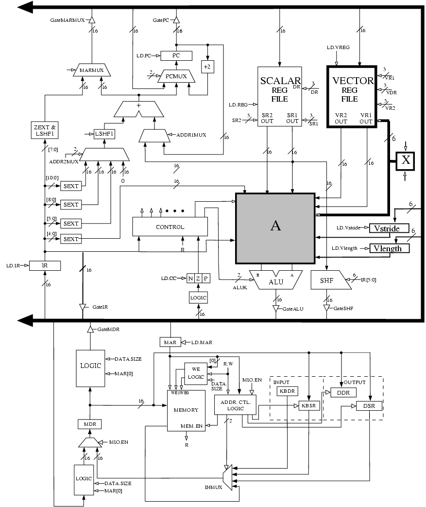
A 6-bit input to the Vector Register file has been labeled X on the datapath diagram. What is the purpose of this input? (Answer in less than 10 words )
The logic structure X contains a 6-bit register and some additional logic. X has two control signals as its inputs. What are these signals used for?
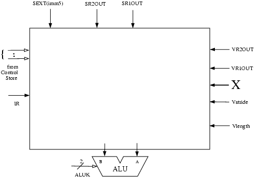
Grey box A contains several additional muxes on both input lines to the ALU. Complete the logic diagram of grey box A (shown below) by showing all muxes and interconnects. You will need to add new signals to the control store; be sure to clearly label them in the logic diagram.
- Keep in mind that we will still need to support all the existing scalar operations.
- The XOR operation in the ALU can be used to compare two values.
- Our solution required 3 additional control signals and 6 2-to-1 muxes.
-
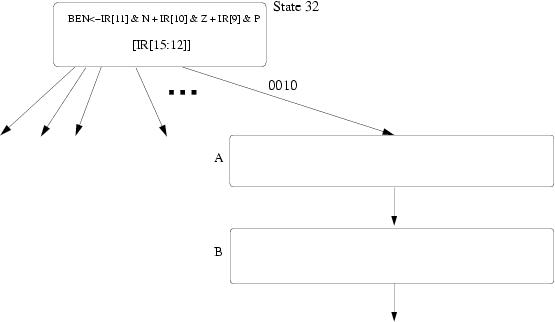
We show the beginning of the state diagram necessary to implement VLD. Using the notation of the LC-3b State Diagram, add the states you need to implement VLD. Inside each state describe what happens in that state. You can assume that you are allowed to make any changes to the microsequencer that you find necessary. You do not have to make/show these changes. You can modify BaseR and the condition codes. Make sure your design works when Vlength equals 0. Full credit will be awarded to solutions that require no more than 7 states.