1) Part a) An instruction set generally consists of three kinds of instructions:
_____operates______, an example of which is ___ADD, AND, NOT___
___data movement___, an example of which is ___LD, LDR, LDI, LEA, ST, STR, STI___
______control______, an example of which is ___TRAP, JMP, BR, RTI, JSR___
1) Part b)If we can implement any logic function using many copies of a single gate (or a
set of gates), then we say that single gate (or set of gates) is
logically complete (or universal)
1) Part c)A ___logical or boolean___ variable is a variable that can have one of exactly two values. It gets its name from the fact that originally the two values were TRUE and FALSE, and the awareness that the value of such a variable must be exactly one of these two values.
1) Part d)If you know that R1 XOR R2 = 0, what can you infer about the contents of any
of the registers R0 to R7?
R1 and R2 must have the same values. Nothing about any of the others.
1) Part e)What logic structure does a mux with the 0 input line tied to the select line
implement? Hint: Fill out the truth table.
If you fill in the truth table, you will see that it is an AND gate.
2) Part a)The following LC-3 instruction is fetched, loaded into the IR, decoded, and executed.
0000 a b c 000000000
    Since adding 0 to the PC does not change the PC, the condition codes provide no useful information
    to THIS particular instruction, which is what the question asked. The hint: "Be careful" in boldface was
    supposed to help.
    Answer (in one word): NOTHING!
2) Part b) The LC-3 has just executed ten instructions. An examination of the behavior during each clock
cycle reveals that exactly one of the ten instructions was a branch (opcode=0000) and the rest were
some number of LDR, LD, and AND instructions. Exactly 16 memory accesses were made during the time
these ten instructions were executed. How many AND instructions were executed?
    10 instructions means 10 instruction fetches from memory. That leaves six. LD and LDR each require
    another memory access to get the data to be loaded. So, there are six loads and one branch. 10-6-1=3.
    Answer: 3.
2) Part c) Your task is to write a program segment of three consecutive LC-3 instructions. The first instruction is to set one of the three condition codes. The second instruction is to set one of the other two condition codes. The third instruction is to set the third condition code. You must use a different opcode in each of the instructions.
The initial state of the LC-3 (i.e. the contents of the registers, memory, etc. prior to the execution of your three instructions) is not known to you.
Note: You must also specify which condition code the instruction sets.
    There were actually several tricky solutions to this.  The simplest untricky one was to recall that
    we can put all 0s in a register by ANDing it with an immediate 0.  We have done this in class many times.

    Therefore, 0101 000 000 1 00000 puts 0 in R0.  Z is set.

    If we then add 1 to R0: 0001 000 000 1 00001, we will have 1 in R0. P is set.

    If we then complement R0: 1001 000 000 111111, we will have xFFFE in R0. N is set.
3) Recall that the standard IEEE 32-bit floating point data type wherein normalized numbers having values (-1)^sign * 1.fraction * 2^(exponent-127) are expressed with 1 bit of sign, 8 bits of exponent, and 23 bits of fraction.
In this problem, we will define an 8-bit floating point data type, where we use 1 bit for the sign, 4 bits for the exponent, using an excess-9 code (i.e., BIAS = 9) and 3 bits of fraction.
3) Part a) Show the representation for 3 1/4 in this data type:
    3 1/4 is 11.01, which is 1.101 * 2^1.  The fraction part (after removing the redundant MSB) is 101.
    The exponent, after adding the bias is ten, or 1010.

    Therefore, the representation is: 0 1010 101.
3) Part b) What is the largest positive normalized number that can be expressed with this 8-bit floating point
data type?
    The largest number would assume the largest exponent and all 1's in the fraction: 0 11l0 111, which
    represents 1.111 * 2^(14-9) = 111100 = 60.
4) Alarm clocks normally ring when the hour reaches a preset time. We would like to design a more sophisticated
alarm clock such that the output (the signal to make the alarm clock ring) occurs as follows:
If it is a weekday (Monday through Friday), we wish the alarm clock to ring when the time reaches 7am. If it is
the weekend (Saturday, Sunday) and the sun is shining, we still wish the alarm clock to ring at 7am so we can play
golf. If the sun is not shining on the weekend, we wish the alarm clockto ring at 9am so we can sleep late. We note
that a simple four-input, one-output logic circuit is sufficient to produce the output that will make the alarm ring.
4) Part a) The four inputs are:
    A: ___weekday___ (no=0, yes=1)
    B: ____sunny____ (no=0, yes=1)
    C: 7am (no=0, yes=1)
    D: 9am (no=0, yes=1)
Depending on the value you chose for weekday vs. weekend and sunny vs. not_sunny, you would get slightly different answers, all of which are fine.
Suppose you say A is weekday = 1, B is sunny = 1.
Then you want the alarm to go off for
     A=1, B=1, C=1, D=0
     A=1, B=0, C=1, D=0
     A=0, B=1, C=1, D=0
     A=0, B=0, C=0, D=1
These input combinations MUST produce an output 1.
Note C=1, D=1 can never occur, so the output for the four input combinations that have C=1, D=1 doesn't matter. We say we "don't care" what the output is for those combinations since they will never occur and so can never make the alarm ring. Any output you chose was fine for these four input combinations that can never occur. All other combinations must give an output 0.
The logic is simply four 4-input AND gates with appropriate bubbles, all of whose outputs are inputs to a 4-input OR gate.
There are simpler logic circuits that you will learn how to construct in EE 316. However, in EE 306, we are not concerned with that.
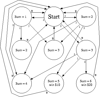
5) A game of chance uses a die (the singular of dice) which has the numbers 1, 2, and 3 on its six faces (two occurrences of each). The game consists of rolling the die twice. If the sum of the two rolls is 6, you win $20. If the sum of the two rolls is 5, you win $10. Else, you win nothing. After the two rolls, you press a button to return to the initial state. Complete a description of the Finite State Machine below to show all possible states, state transitions, and outputs. Clearly label the outputs associated with each state.
There are several correct solutions here as well. The most important thing to remember is that after you roll the die once, you have to store the result of that first roll. We do that by going to a new state, in the same way we did with the coke machine.
It is not okay to say, we are in state Start and we roll the die twice. That runs contrary to the whole notion of the state machine, which you should not have had a problem with IF you did the coke machine problem in the homework.
Each state has four inputs: roll a 1, a 2, a 3, or push the button. Each state should clearly identify the input that is causing each state transition.
The simplest solution is to identify a state for each number that you have accumulated by your rolls. So, after the first roll, you go to the state labeled 1, or 2, or 3. After the second roll, you go to the state labeled 2, or 3, or 4, or 5, or 6, depending on what state you were in after the first roll and what the second roll was. Inside state 5, you should put $10 and inside state 6, you should put $20. From all states you should have an arc back to Start if you hit the pushbutton.
There are subtler solutions that we will expect of you after EE 316, but not now.
6) Listed below are the states of the registers of the LC-3 at two times during the execution of a single instruction. Given the information provided, fill in all 16 bits of the instruction that is being executed.
The instruction being executed is stored in location x3000 in memory. The first state is just after the instruction has been fetched and stored in the IR. The second state is at the end of the execution of the instruction, before the next instruction is fetched.
Note: Some data has been intentionally left out.
    Register    After Fetch    At End
         PC           x3001          x3001
	 MAR	      x3000	     x4020
	 MDR	      x6???	     X0000
	 R0           x5000	     x0000
	 R1	      x4000	     x4000
	 R2	      x3000	     x3000
	 R3	      x2000	     x2000
	 R4	      x1000	     x1000
	 R5	      x4040	     x4040
	 R6	      x5050	     x5050
	 R7	      x6060	     x6060
The idea here is to systematically examine what is given until you arrive at the solution. We gave you the high hex digit in the MDR (a 6) identifying the opcode as 0110 (LDR). We note that the state of the registers at the end of the instruction are the same as at the end of the fetch phase except for R0, which contains 0. This means that the destination register of the LDR must have been R0. We note that after fetch, the MAR contains x3000, but at the end of the instruction, the MAR contains x4020. This means x3000 contains the instruction fetched, and MAR contains the address of the location that must be read to get the value to load into R0. Since that location is x4020, it must have been constructed from adding BaseR to the sign-extended offset. Examining all the registers as a possible BaseR, the only one that can work is R5, with an offset of xFFE0 (i.e., - hex 0020).
Therefore, the instruction is: 0110 000 101 100000
Rhetorical question: Why does not R1 work as the BaseR?