Perform the following logical operations. Express your answers in hexadecimal notation.
- xABCD OR x9876 xBBFF
- x1234 XOR x1234 x0000
- xFEED AND (NOT(xBEEF)) x4000
Fill in the truth table for the equations given. The first line is done as an example.
Q2 = NOT ((Y OR Z) AND (X AND Y AND Z))
          X    Y    Z   | Q1    Q2
         --------------------------
          0    0    0   |  0    1
          0    0    1   |  0    1
          0    1    0   |  0    1
          0    1    1   |  0    1
          1    0    0   |  1    1
          1    0    1   |  1    1
          1    1    0   |  1    1
          1    1    1   |  0    0
A<=Has Professor Patt been uncomfortably warm this summer?
B<=Does Professor Patt want a new, fresher look?
C<=Are beards cool?
We think that Professor Patt should shave his beard if he has been uncomfortably warm this summer. He should also shave his beard if he wants a new fresher look and beards are not cool.
Write the logic equation for Y in terms of A,B,C that solves this problem, and draw the gate-level diagram.
Y = A OR (B AND (NOT C))
- Draw a transistor-level diagram for a three-input AND gate and a three-input OR gate. Do this by extending the designs from Figures 3.6a and 3.7a. (Figures can be found in the book on pages 56 & 57 respectively). For 3-input OR gate: Add one P-type transistor from Vdd to C, in series to the current gate, and one N-type from C to GROUND, in parallel to the current gate.
- Replace the transistors in your diagrams from part (a)
with either a wire or no wire to reflect the circuit’s operation when
the following inputs are applied:
-
A = 1, B = 0, C = 0
Output of 3-input OR will be 1, Output of 3-input AND will be 0.
- The transistor circuit shown below produces the accompanying truth table. The inputs to some of the gates of the transistors are not specified. Also, the outputs for some of the input combinations of the truth table are not specified. Complete both specifications. i.e., all transistors will have their gates properly labeled with either A, B, or C,
and all rows of the truth table will have a 0 or 1 specified as the output.
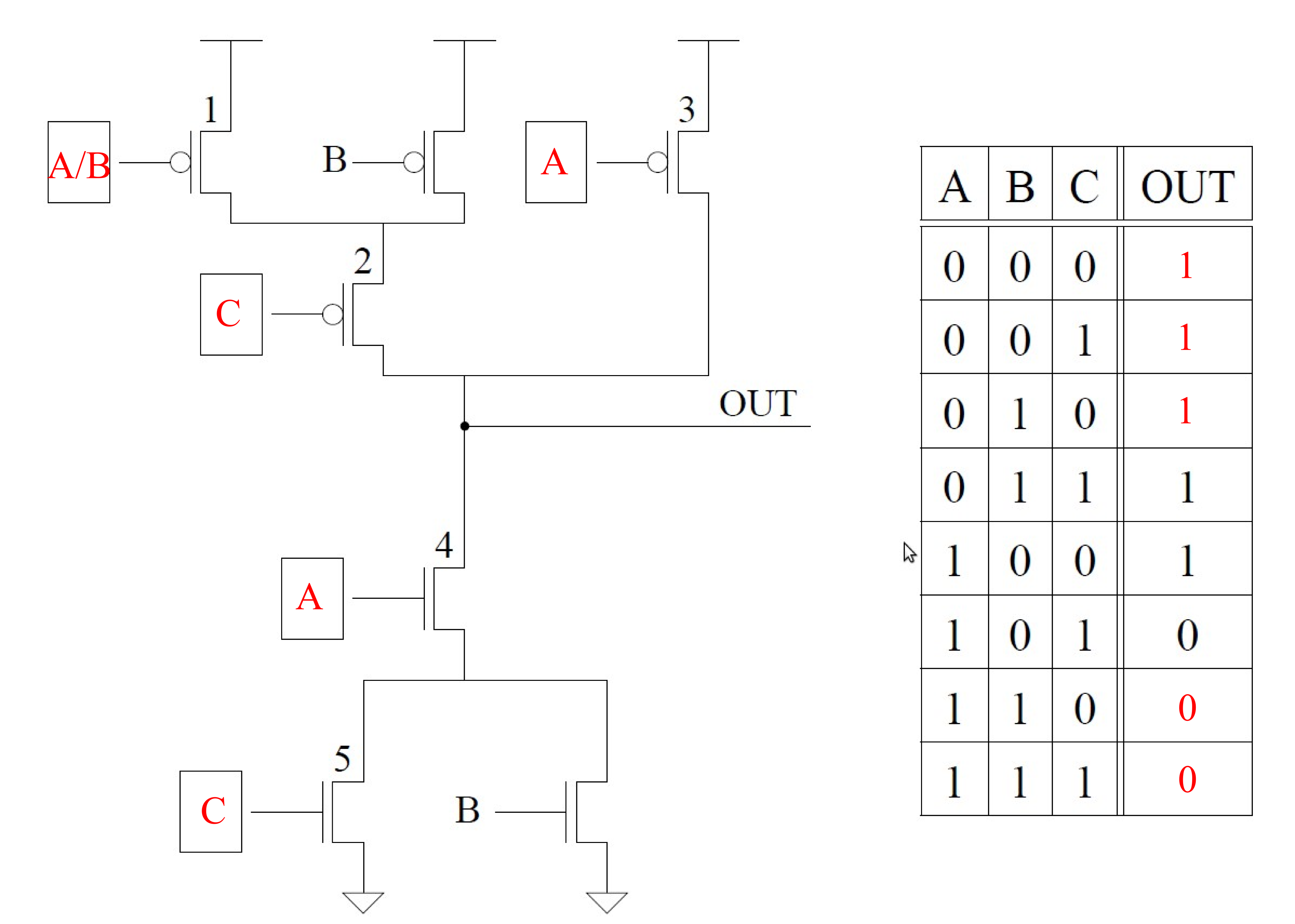
Figure 1
For 3-input AND gate: Add one P-type transistor from Vdd to C, in parallel to the current gates, and one N-type from C to GROUND, in series to the current gates.
For example, in part a, the missing item is X. That is 0 OR 0 = 0 and 0 OR 1 = 1.
- 0 OR X = ___
X - 1 OR X = ___
1 - 0 AND X = ___
0 - 1 AND X = ___
X - __ XOR X = X
0
Logic circuit 1 in Figure 3.36 (page 87 of the book) has inputs A, B, C. Logic circuit 2 in Figure 3.37 (page 87 of the book) has inputs A and B. Both logic circuits have an output D. There is a fundamental difference between the behavioral characteristics of these two circuits. What is it? Hint: What happens when the voltage at input A goes from 0 to 1 in both circuits?
Figure 3.36 is a 2-input mux, which conbinational logic i.e., D is the output of the circuit.
Figure 3.37 is a storage element, which stores the data value previously stored in the latch.
A) Implement a 4-to-1 mux using only 2-to-1 muxes making sure to properly connect all of the terminals. Remember that you will have 4 inputs (A, B, C, and D), 2 control signals (S1 and S0), and 1 output (OUT). After implementing the 4-1 mux, fill in the truth table below.
   A      B		        C      D
 __|______|__	              __|______|__
 \ 0      1  /	              \ 0      1  /
  \_________/<------ S0        \_________/<------ S0
       |_____________      _________|
                  ___|_____|__
                  \  0     1 /
                   \________/<------ S1
                       |
                       F
You require 3 muxes. First, the input are A and B and the select line is S0. Second, inputs are C and D and the select line is also S0. Third, is a mux where both its inputs are the outputs of the first two muxes and select line is S1. Every time S1 and S0 are both 0, OUT is the same as A.
Every time S1 and S0 are 0 and 1 respectively, OUT is the same as B.
Every time S1 and S0 are 1 and 0 respectively, OUT is the same as C.
Every time S1 and S0 are 1 and 1 respectively, OUT is the same as D.
B) Implement F = A xor B using ONLY two 2-to-1 muxes. You are not allowed to use a not gate (A' and B' are not available).
         1      0
       __|______|__
       \ 0      1  /
        \_________/<------ B
      B     |
   ___|_____|__
   \  0     1 /
    \________/<------ A
         |
         F
Say the speed of a logic structure depends on the largest number of logic gates through which any of the inputs must propagate to reach an output. Assume that a NOT, an AND, and an OR gate all count as one gate delay. For example, the propagation delay for a two-input decoder shown in Figure 3.11 is 2 because some inputs propagate through two gates.
- What is the propagation delay for the two-input mux shown in Figure 3.12 (page 61)? 3
- What is the propagation delay for the 4-bit adder shown in Figure 3.16 (page 63)? 12
-
Can you reduce the propagation delay for the circuit shown in Figure 3
by implementing the equation in a different way? If so, how?
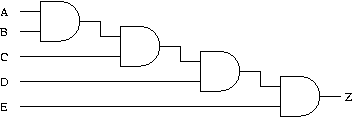
Figure 3
You can construct a tree-like structure.
E = ((A AND B) AND (C AND D) ) AND E)
Recall that the adder was built with individual "slices" that produced a sum bit and carryout bit based on the two operand bits A and B and the carryin bit. We called such an element a full-adder. Suppose we have a 3-to-8 decoder and two six-input OR gates, as shown in Figure 3 below. Can we connect them so that we have a full-adder? If so, please do. (Hint: If an input to an OR gate is not needed, we can simply put an input 0 on it and it will have no effect on anything. For example, see the figure below.)
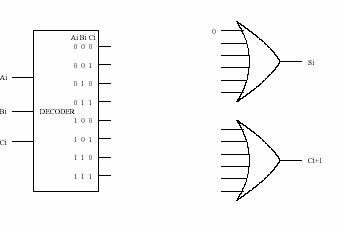
Figure 3
For the OR gate generating the Ci+1, connect the 4 outputs: 011, 101, 110, and 111 from the decoder to the OR gate. Connect the remaining 2 inputs of the OR gate to 0.
Design the combinational logic circuit for an elevator controller such that the
option to go up or down by only one floor is disabled. Assume that the building
the elevator is in has 4 floors. Your inputs are the current floor and the next
requested floor. The output from the controller should be the next floor to go
to. Please show the full truth table for the elevator controller.
Since there are four floors, you will need 2 bits to represent a floor. Let
the logic variable C[1:0] represent the current floor, R[1:0] represent the
requested floor, and D[1:0] represent the floor the elevator should go to
given a current floor and a requested floor. Shown below is the truth table
for this combinational logic circuit.
C1 C0 R1 R0 | D1 D0
-------------------
0  0  0  0  | 0  0
0  0  0  1  | 0  0
0  0  1  0  | 1  0
0  0  1  1  | 1  1
0  1  0  0  | 0  1
0  1  0  1  | 0  1
0  1  1  0  | 0  1
0  1  1  1  | 1  1
1  0  0  0  | 0  0
1  0  0  1  | 1  0
1  0  1  0  | 1  0
1  0  1  1  | 1  0
1  1  0  0  | 0  0
1  1  0  1  | 0  1
1  1  1  0  | 1  1
1  1  1  1  | 1  1
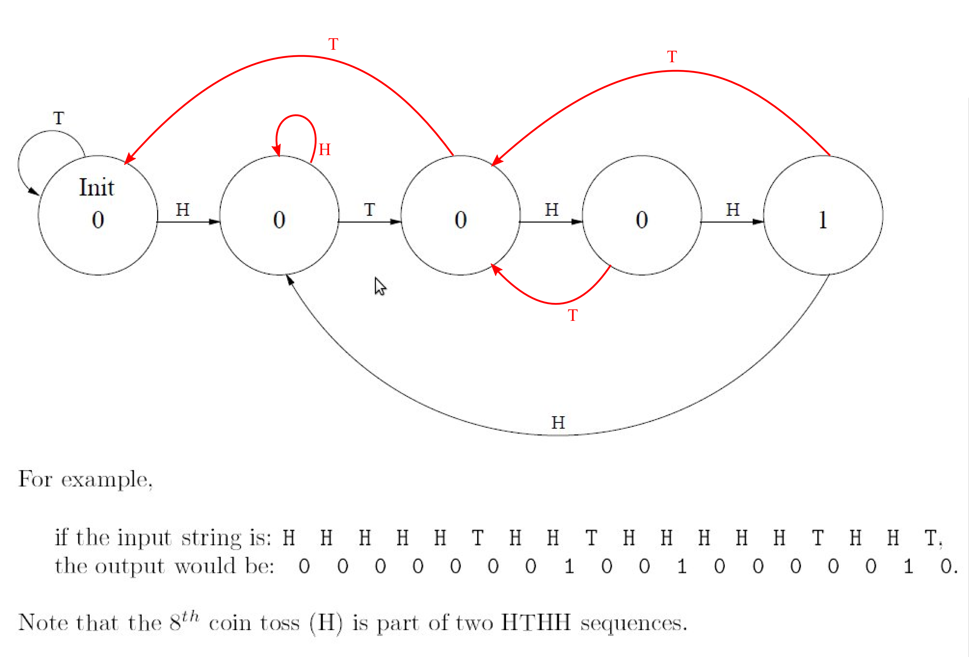
Shown below is a partially completed state diagram of a finite state machine that takes an input string of H (heads) ant T (tails) and produces an output of 1 every time the string HTHH occurs.
- Complete the state diagram of the finite state machine that will do this for any input sequence of any length Completed state machine is shown in the figure below
- If this state machine is implemented with a sequential logic circuit how many state variables will be needed? 3 bits
We want to make a state machine for the scoreboard of the Texas vs. Oklahoma Football game. The following information is required to determine the state of the game:
1. Score: 0 to 99 points for each team
2. Down: 1, 2, 3, or 4
3. Yards to gain: 0 to 99
4. Quarter: 1, 2, 3, 4
5. Yardline: any number from Home 0 to Home 49, Visitor 0 to Visitor 49, 50
6. Possesion: Home, Visitor
7. Time remaining: any number from 0:00 to 15:00, where m:s (minutes, seconds)
(a) What is the minimum number of bits that we need to use to store the state required?
(b) Suppose we make a separate logic circuit for each of the seven elements on the scoreboard, how many bits would it then take to store the state of the scoreboard?
(c) Why might part b be a better way to specify the state?
A logic circuit consisting of 6 gated D latches and 1 inverter is shown below:
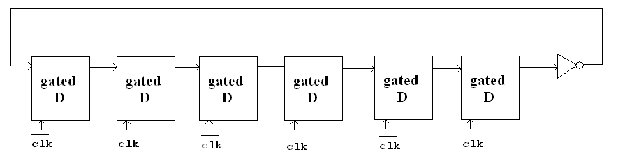
Figure 1
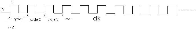
Figure 2
Question: What is the state after 50 cyles. How many cycles does it take for a specific state to show up again?
(3.31)
If a particular computer has 8 byte addressability and a 4 bit address space,
how many bytes of memory does that computer have?
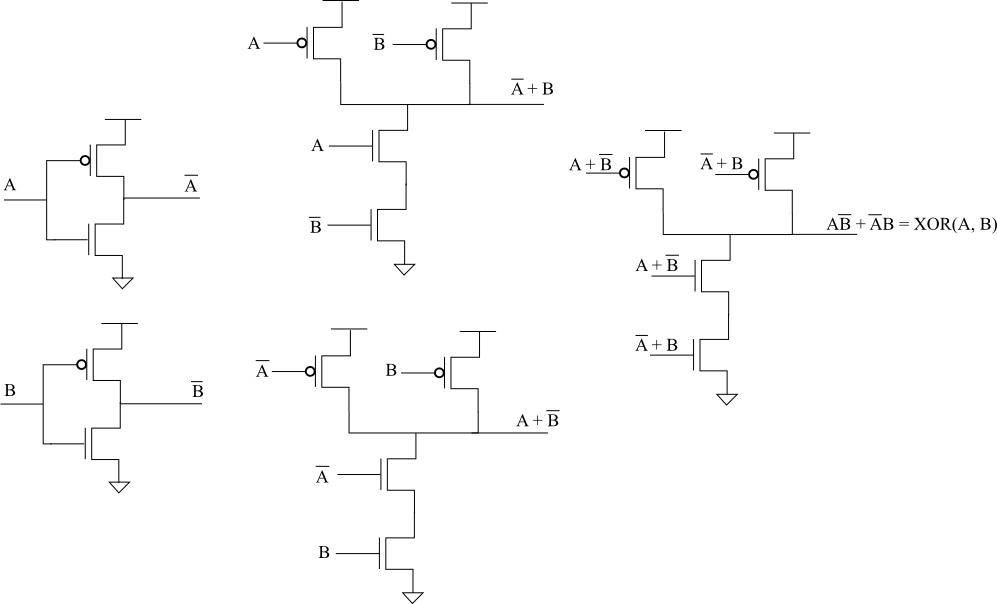
Draw the transistor level circuit of a 2 input XOR gate