Department
of Electrical and Computer Engineering
The
University of Texas at Austin
EE 306, Fall 2013
Problem Set 3
Due: 7 October, before class
Yale N. Patt, Instructor
TAs: Ben Lin, Mochamad Asri,
Ameya Chaudhari, Nikhil Garg, Lauren Guckert,
Jack Koenig, Saijel Mokashi, Sruti Nuthalapati, Sparsh Singhai, Jiajun Wang
Instructions:
You are encouraged to work on the problem set in groups and turn in one problem
set for the entire group. Remember to put all your names on the solution sheet.
Also, remember to put the name of the TA and the time for the discussion
section you would like the problem set turned back to you. Show your work.
1. Elevator Problem Revisited
Recall the elevator controller problem on Problem Set 2. You were asked to
design the truth table for an elevator controller such that the option to move
up or down by one floor is disabled. If there is a request to move only one
floor or to move zero floors, the elevator should remain on the current floor.
For this problem, you will design the state machine for the sequential logic
circuit for an elevator controller which performs the same operation. You can
assume that the building the elevator is in has 4 floors. The input to the
state machine is the next requested floor. There will be a state for each floor
the elevator could be on. Draw a finite state machine that describes the
behavior of the elevator controller. How many bits are needed for the inputs?
- (3.33)
Using Figure 3.21 on page 69 in the book, the diagram of the, 22-by-3-bit memory. - To read from the fourth
memory location, what must the values of
A[1:0]andWEbe? - To change the number of
locations in the memory from 4 to 60, how many address lines would be
needed? What would the addressability of the memory be after this change
was made?
- Suppose the width (in
bits) of the program counter is the minimum number of bits needed to
address all 60 locations in our memory from part (b). How many additional
memory locations could be added to this memory without having to alter
the width of the program counter?
3. The figure below is a diagram of a 22-by-16-bit
memory, similar in implementation to the memory of Figure 3.21 in the textbook.
Note that in this figure, every memory cell represents 4 bits of storage
instead of 1 bit of storage. This can be accomplished by using 4 Gated-D
Latches for each memory cell instead of using a single Gated-D Latch. The hex
digit inside each memory cell represents what that cell is storing prior to
this problem.
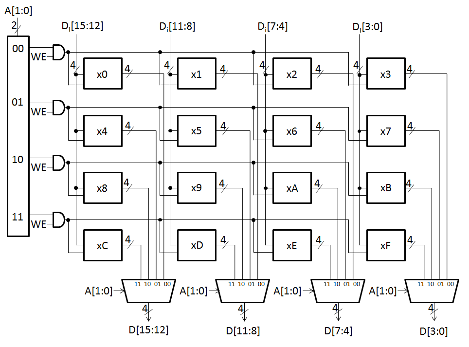
Figure 3: 22-by-16 bit memory
- What is the address space
of this memory?
- What is the
addressability of this memory?
- What is the total size
in bytes of this memory?
- This memory is accessed
during four consecutive clock cycles. The following table lists the
values of some important variables just before the end of the cycle
for each access. Each row in the table corresponds to a memory access.
The read/write column indicates the type of access: whether the access is
reading memory or writing to memory. Complete the missing entries in the
table.
|
WE |
A[1:0] |
Di[15:0] |
D[15:0] |
Read/Write |
|
|
|
|
||
|
|
|
|
||
|
|
|
|
||
|
|
|
|
4. (3.41)
The IEEE campus society office sells sodas for 35 cents. Suppose they install a
soda controller that only takes the following three inputs: nickel, dime, and
quarter. After you put in each coin, you push a pushbutton to register the
coin. If at least 35 cents has been put in the controller, it will output a
soda and proper change (if applicable). Draw a finite state machine that
describes the behavior of the soda controller. Each state will represent how
much money has been put in (Hint: There will be seven of those states). Once
enough money has been put in it, the controller will go to a final state where
the person will receive a soda and proper change (Hint: There are five such
final states). From the final state, the next coin that is put in will start
the process again, contributing to the next purchase.
5.
(Adapted from 3.30)
A comparator circuit has two 1-bit inputs, A and B, and three 1-bit outputs, G
(greater), E (equal), and L (less than). Refer to figures 3.40 and 3.41 on page
92 in the book for this problem.
- Draw the truth table
for a 1-bit comparator.
- Implement G, E and L
for a 1-bit comparator using AND, OR, and NOT gates.
- Figure
3.41 performs one-bit comparisons of the corresponding bits of two
unsigned integer A[3:0] and B[3:0]. Using the 12 one-bit results of these
4 one-bit comparators, construct a logic circuit to output a 1 if
unsigned integer A is larger than unsigned integer B (the logic circuit
should output 0 otherwise). The inputs to your logic circuit are the outputs of the
4 one-bit comparators and should be labeled G[3], E[3], L[3], G[2], E[2],
L[2], ... L[0]. (Hint: You may not need to use all 12 inputs.)
- Suppose that an
instruction cycle of the LC-3 has just finished and another one is about
to begin. The following table describes the values in select LC-3
registers and memory locations:
|
Register |
Value |
|
|
|
|
|
|
|
|
|
|
|
|
|
|
|
|
|
|
|
|
|
|
|
|
|
|
|
|
|
|
|
Memory Location |
Value |
|
|
|
|
|
|
|
|
|
|
|
|
For each phase of the new
instruction cycle, specify the values that PC, IR,
MAR, MDR, R1, and R2 will have at the
end of the phase in the following table:
|
|
|
|
|
|
|
|
|
|
|
|
|
|
|
Fetch |
||||||||||||
|
Decode |
||||||||||||
|
Evaluate
Address |
||||||||||||
|
Fetch Operands |
||||||||||||
|
Execute |
||||||||||||
|
Store Result |
Hint: Example 4.2 on page 104
illustrates the LDR instruction of the LC-3. Notice that values of memory
locations x3000, and 3003 can be interpreted as
LDR instructions.
- (4.8)
Suppose a 32-bit instruction has the following format:
|
|
|
|
|
|
If there are 255 opcodes and 120 registers, and every register is available
as a source or destination for every opcode,
- What is the minimum
number of bits required to represent the
OPCODE? - What is the minimum
number of bits required to represent the Destination Register (
DR)? - What is the maximum
number of
UNUSEDbits in the instruction encoding?