Consider the following piece of code:
for(i = 0; i < 100; i++)
  A[i] = ((B[i] * C[i]) + D[i]) / 2;
Translate this code into assembly language using the following instructions in the ISA (note the number of cycles each instruction takes is shown with each instruction):
Opcode Operands Number of Cycles Description LEARi, X1 Ri ← address of X LDRi, Rj, Rk11 Ri ← MEM[Rj + Rk] STRi, Rj, Rk11 MEM[Rj + Rk] ← Ri MOVIRi, Imm1 Ri ← Imm MULRi, Rj, Rk6 Ri ← Rj × Rk ADDRi, Rj, Rk4 Ri ← Rj + Rk ADDRi, Rj, Imm4 Ri ← Rj + Imm RSHFARi, Rj, amount1 Ri ← RSHFA (Rj, amount) BRccX1 Branch to X based on condition codes Assume it takes one memory location to store each element of the array. Also assume that there are 8 registers (R0-R7).
How many cycles does it take to execute the program?
-
Now write Cray-like vector/assembly code to perform this operation in the shortest time possible. Assume that there are 8 vector registers and the length of each vector register is 64. Use the following instructions in the vector ISA:
Opcode Operands Number of Cycles Description LDVst, #n1 Vst ← n LDVln, #n1 Vln ← n VLDVi, X + offset11, pipelined VSTVi, X + offset11, pipelined VmulVi, Vj, Vk6, pipelined VaddVi, Vj, Vk4, pipelined VrshfaVi, Vj, amount1 How many cycles does it take to execute the program on the following processors? Assume that memory is 16-way interleaved.
- Vector processor without chaining, 1 port to memory (1 load or store per cycle)
- Vector processor with chaining, 1 port to memory
- Vector processor with chaining, 2 read ports and 1 write port to memory
Little Computer Inc. is now planning to build a new computer that is more suited for scientific applications. LC-3b can be modified for such applications by replacing the data type Byte with Vector. The new computer will be called LmmVC-3 (Little 'mickey mouse' Vector Computer 3). Your job is to help us implement the datapath for LmmVC-3. LmmVC-3 ISA will support all the scalar operations that LC-3b currently supports except the LDB and STB will be replaced with VLD and VST respectively. Our datapath will need to support the following new instructions:
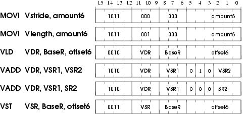
Note: VDR means “Vector Destination Register” and VSR means “Vector Source Register.”
- MOVI
- If IR[11:9] = 000, MOVI moves the unsigned quantity amount6 to Vector Stride Register (Vstride). If IR[11:9] = 001, MOVI moves the unsigned quantity amount6 to Vector Length Register (Vlength). This instruction has already been implemented for you.
- VLD
- VLD loads a vector of length Vlength from memory into VDR. VLD uses the opcode previously used by LDB. The starting address of the vector is computed by adding the LSHF1(SEXT(offset6)) to BaseR. Subsequent addresses are obtained by adding LSHF1(ZEXT(Vstride)) to the address of the preceding vector element.
- VST
- VST writes the contents of VSR into memory. VST uses the opcode previously used by STB. Address calculation is done in the same way as for VLD.
- VADD
- If IR[4] is a 1, VADD adds two vector registers (VSR1 and VSR2) and stores the result in VDR. If IR[4] is a 0, VADD adds a scalar register (SR2) to every element of VSR and stores the result in VDR.
VLD, VST, and VADD do not modify the content of Vstride and Vlength registers.
The following five hardware structures have been added to LC-3b in order to implement LmmVC-3.
- Vector Register File with eight 63-element Vector registers
- Vector Length Register
- Vector Stride Register
- A third input to DRMUX containing IR[8:6]
- Grey box A
- Box labeled X
These structures are shown in the LmmVC-3 datapath diagram:
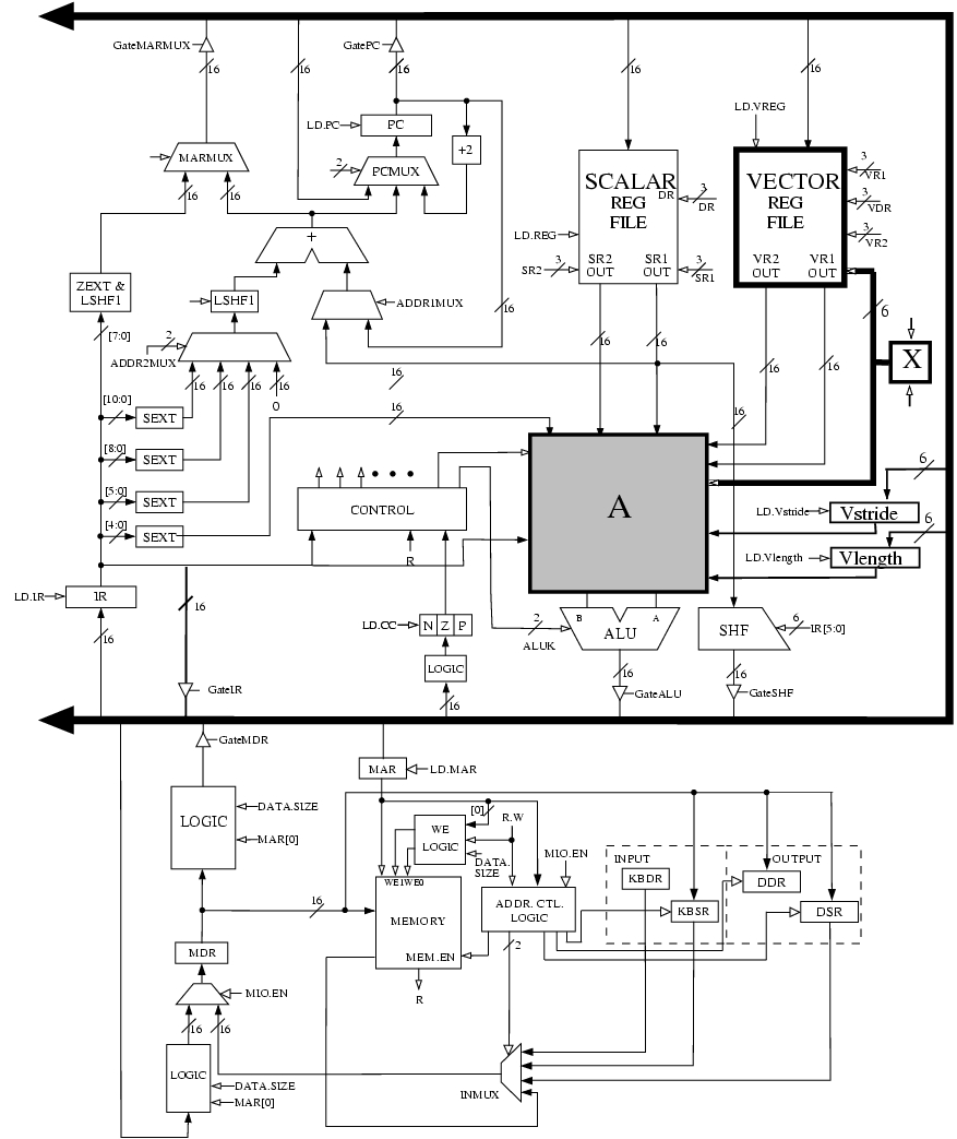
A 6-bit input to the Vector Register file has been labeled X on the datapath diagram. What is the purpose of this input? (Answer in less than 10 words )
The logic structure X contains a 6-bit register and some additional logic. X has two control signals as its inputs. What are these signals used for?
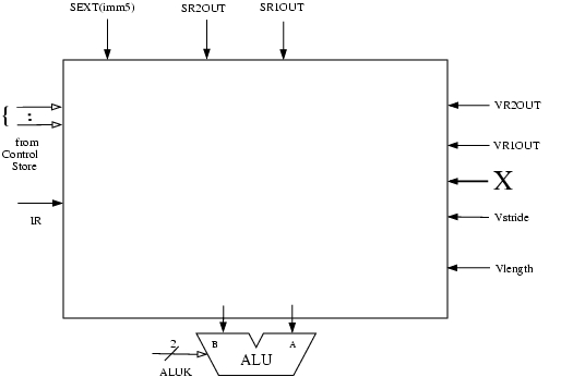
Grey box A contains several additional muxes on both input lines to the ALU. Complete the logic diagram of grey box A (shown below) by showing all muxes and interconnects. You will need to add new signals to the control store; be sure to clearly label them in the logic diagram.
- Keep in mind that we will still need to support all the existing scalar operations.
- The XOR operation in the ALU can be used to compare two values.
- Our solution required 3 additional control signals and 6 2-to-1 muxes.
-
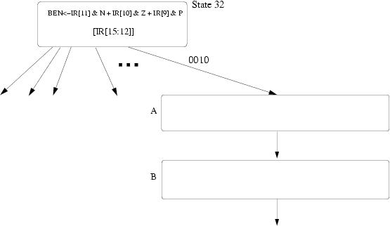
We show the beginning of the state diagram necessary to implement VLD. Using the notation of the LC-3b State Diagram, add the states you need to implement VLD. Inside each state describe what happens in that state. You can assume that you are allowed to make any changes to the microsequencer that you find necessary. You do not have to make/show these changes. You can modify BaseR and the condition codes. Make sure your design works when Vlength equals 0. Full credit will be awarded to solutions that require no more than 7 states.
Consider the following piece of code:
     for(i = 0; i < 8; ++i){
       for(j = 0; j < 8; ++j){
         sum = sum + A[i][j];
       }
     }
The figure below shows an 8-way interleaved, byte-addressable memory. The total size of the memory is 4KB. The elements of the 2-dimensional array, A, are 4-bytes in length and are stored in the memory in column-major order (i.e., columns of A are stored in consecutive memory locations) as shown. The width of the bus is 32 bits, and each memory access takes 10 cycles.
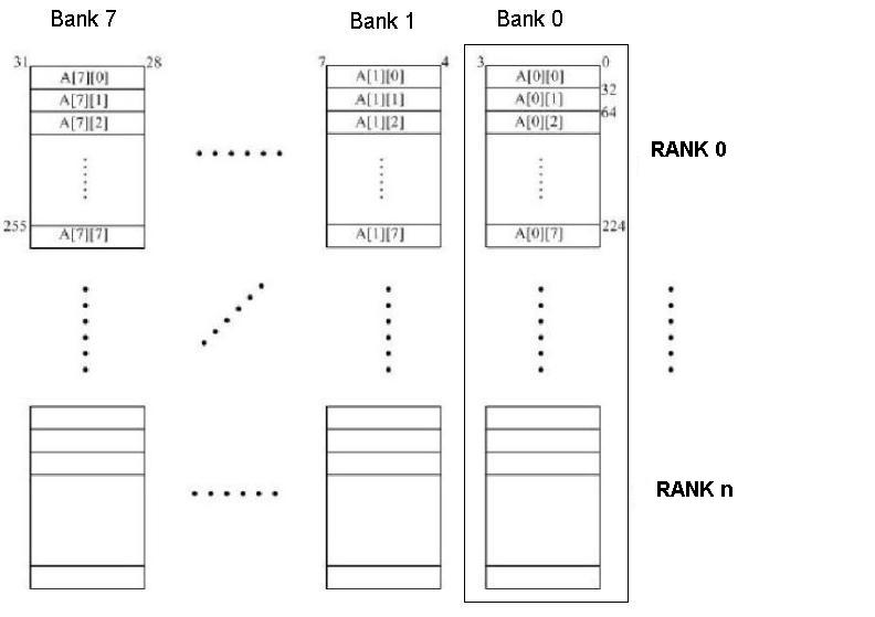
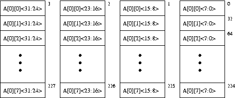
A more detailed picture of the memory chips in Rank 0 of Bank 0 is shown below.
Since the address space of the memory is 4KB, 12 bits are needed to uniquely identify each memory location, i.e.,
Addr[11:0]. Specify which bits of the address will be used for:- Byte on bus
Addr[_____:_____]
- Interleave bits
Addr[_____:_____]
- Chip address
Addr[_____:_____]
- Rank bits
Addr[_____:_____]
- Byte on bus
How many cycles are spent accessing memory during the execution of the above code? Compare this with the number of memory access cycles it would take if the memory were not interleaved (i.e., a single 4-byte wide array).
Can any change be made to the current interleaving scheme to optimize the number of cycles spent accessing memory? If yes, which bits of the address will be used to specify the byte on bus, interleaving, etc. (use the same format as in part a)? With the new interleaving scheme, how many cycles are spent accessing memory? Remember that the elements of A will still be stored in column-major order.
Using the original interleaving scheme, what small changes can be made to the piece of code to optimize the number of cycles spent accessing memory? How many cycles are spent accessing memory using the modified code?
The figure below illustrates the logic and
memory to support 512 MB (byte addressable) of physical memory, supporting
unaligned accesses. The ISA contains LDByte, LDHalfWord, LDWord,
STByte , STHalfWord and STWord instructions, where a word is 32 bits. Bit 28
serves as a chip enable (active high). If this bit is high the data of the
memory is loaded on the bus, otherwise the output of the memory chip floats (tri-stated).
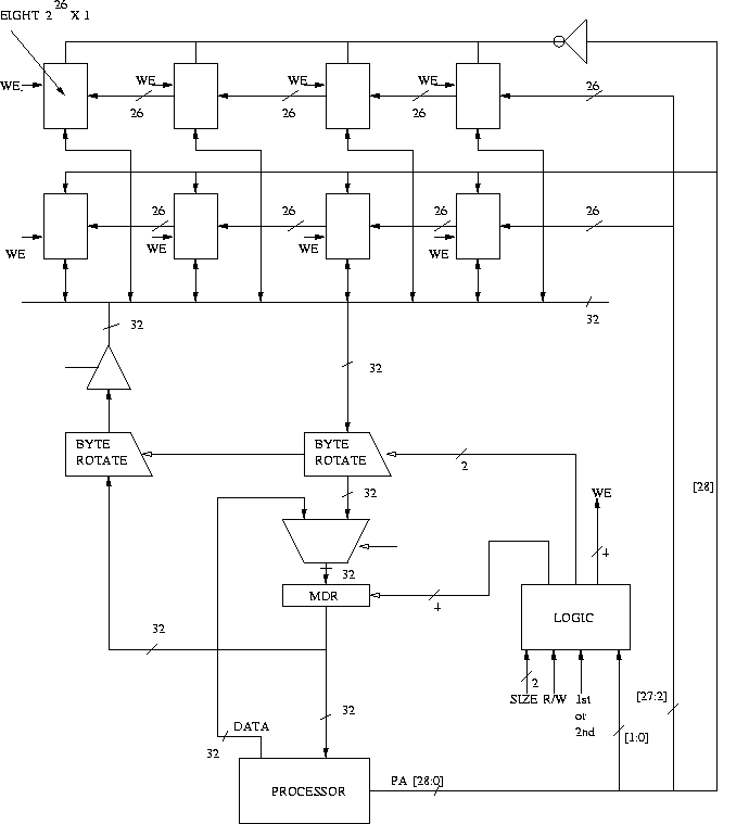
Note: the byte rotators in the figure are right rotators.
Construct the truth table to implement the LOGIC block, having inputs SIZE, R/W,
1st or 2nd access, PHYS_ADDR[1:0] and the outputs shown in the above figure. Assume
that the value of SIZE can be Byte (00), HalfWord (01), and Word (10). Clearly
explain what function each output serves.
If the latency of a DRAM memory bank is 37 cycles, into how many banks would you interleave this memory in order to fully hide this latency when making sequential memory accesses?