Assume the destination register is indicated first, followed by the source(s).
(As stated in the question, cycle counts assume a 16-way interleaved memory so that a new access can be started each cycle. Also, the adder and multiplier are pipelined.)
-
Scalar processor (one of the possible solutions)
          MOVI   R0, 0            (1 cycle)
          LEA    R4, A            (1 cycle)
          LEA    R5, B            (1 cycle)
          LEA    R6, C            (1 cycle)
          LEA    R7, D            (1 cycle)
    LOOP  LD     R1, R5, R0       (11 cycles)
          LD     R2, R6, R0       (11 cycles)
          LD     R3, R7, R0       (11 cycles)
          MUL    R1, R1, R2       (6 cycles)
          ADD    R1, R1, R3       (4 cycles)
          RSHFA  R1, R1, 1        (1 cycle)
          ST     R1, R4, R0       (11 cycles)
          ADD    R0, R0, 1        (4 cycles)
          ADD    R1, R0, -100     (4 cycles)
          BNZ    LOOP             (1 cycle)
5 × 1 + 100 × (11 + 11 + 11 + 6 + 4 + 1 + 11 + 4 + 4 + 1) = 6405 cycles Vector Processor:
The loop could be split into two parts as 64 and 36. Assume the vector code looks as follows: (This solution assumes that the addressing mode VLD V0, B+64 exists - if it doesn't, then you would need 4 + 3 cycles using a pipelined adder to add 64 to A,B,C,D)
LD Vln, #64 (1 cycle) LD Vst, #1 (1 cycle) VLD V0, B (11 + 63 cycles) VLD V1, C (11 + 63 cycles) Vmul V2, V0, V1 (6 + 63 cycles) VLD V3, D (11 + 63 cycles) Vadd V4, V2, V3 (4 + 63 cycles) Vrshfa V5, V4, 1 (1 + 63 cycles) VST V5, A (11 + 63 cycles) LD Vln, #36 (1 cycle) VLD V0, B+64 (11 + 35 cycles) VLD V1, C+64 (11 + 35 cycles) Vmul V2, V0, V1 (6 + 35 cycles) VLD V3, D+64 (11 + 35 cycles) Vadd V4, V2, V3 (4 + 35 cycles) Vrshfa V5, V4, 1 (1 + 35 cycles) VST V5, A+64 (11 + 35 cycles)-
Vector processor without chaining (vector instructions done serially)
First part:
|-1-|-1-|--11--|---63---|--11--|---63---|-6-|---63---|--11--|---63---|-4-|---63---|-1-|---63---|--11--|---63---|
Second part:
|-1-|--11--|--35--|--11--|--35--|-6-|--35--|--11--|--35--|-4-|--35--|-1-|--35--|--11--|--35--|
2 + (74 × 4 + 69 + 67 + 64) + 1 + (46 × 4 + 41 + 39 + 36) = 799 cycles -
Vector processor with chaining, 1 port to memory.
Chaining means the machine begins the next operation as soon as the operands are ready.
 |-1-|-1-|--11--|---63---|--11--|---63---|--11--|---63---|--11--|---63---|--11--|--35--|--11--|--35--|--11--|--35--|--11--|--35--|
                                |-6-|---63---|  |-4-|---63---|                                |-6-|--35--|  |-4-|--35--|
                                                    |-1-|---63---|                                              |-1-|--35--|
                                                           |-1-|
Chaining, in this instance, hides the VMULT, VADD, and VSHL operations. Memory becomes the primary bottleneck.
482 cycles -
Vector processor with chaining; 2 loads, 1 store per cycle.
 |-1-|-1-|--11--|---63---|       VLD V0, B
          |--11--|---63---|       VLD V1, C
                 |-6-|---63---|
                         |--11--|---------------63-----------------|     VLD V3, D  Needs to wait until VLD B is finished
                                |-4-|---63---|
                                    |-1-|---63---|
                                        |--11--|----------------63-----------------|      VST V5,A
                                          |-1-|--11--|---35---|         VLD V0, B+64 (this finishes sooner than VLD D)
                                                              |--11--|----35----|           VLD V1, C+64 Needs to wait for VLF B+64
                                                                     |-6-|----35----|
                                                                         |--11--|--35--|
                                                                                |-4-|--35--|
                                                                                    |-1-|--35--|
                                                                                        |--11--|--35--|
#cycles = 1 + 1 + (11 + 63) + 11 + 4 + 1 + 1 + 1 + (11 + 35) + 11 + 6 + 11 + 4 + 1 + (11 + 35) = 219 cycles
Another solution is to split the loop into two equal parts as 50 and 50.
LD Vln, #50 (1 cycle) LD Vst, #1 (1 cycle) VLD V0, B (11 + 49 cycles) VLD V1, C (11 + 49 cycles) Vmul V2, V0, V1 (6 + 49 cycles) VLD V3, D (11 + 49 cycles) Vadd V4, V2, V3 (4 + 49 cycles) Vrshfa V5, V4, 1 (1 + 49 cycles) VST V5, A (11 + 49 cycles) VLD V0, B+50 (11 + 49 cycles) VLD V1, C+50 (11 + 49 cycles) Vmul V2, V0, V1 (6 + 49 cycles) VLD V3, D+50 (11 + 49 cycles) Vadd V4, V2, V3 (4 + 49 cycles) Vrshfa V5, V4, 1 (1 + 49 cycles) VST V5, A+50 (11 + 49 cycles)-
Vector processor without chaining (vector instructions done serially)
First part:
|-1-|-1-|--11--|---63---|--11--|---63---|-6-|---63---|--11--|---63---|-4-|---63---|-1-|---63---|--11--|---63---|
Second part:
|--11--|--35--|--11--|--35--|-6-|--35--|--11--|--35--|-4-|--35--|-1-|--35--|--11--|--35--|
2 + (74 × 4 + 69 + 67 + 64) + (46 × 4 + 41 + 39 + 36) = 798 cycles -
Vector processor with chaining, 1 port to memory. This part for solution B will be the same as solution B. Total = 482 cycles
-
Vector processor with chaining; 2 loads, 1 store per cycle
 |-1-|-1-|-11-|-----49-----|
          |-11-|-----49-----|
               |-6-|-----49-----|
                           |-11-|-----49-----|   ** LD D would need to wait for LD B to finish
                                |-4-|-----49-----|
                                    |-1-|-----49-----|
                                        |-11-|-----49-----|
                                         |-11-|-----49-----|
                                             |-11-|-----49-----|  ** LD C+50 would need to wait till the LD D from the first part finishes
                                                  |-6-|-----49-----|
                                                           |-11-|-----49-----|  ** LD D+50 would need to wait for LD B+50 to finish
                                                                |-4-|-----49-----|
                                                                    |-1-|-----49-----|

                                                                        |-11-|-----49-----|
1 + 1 + (11 + 49) + 11 + 4 + 1 + 1 + (11 + 49) + 11 + 4 + 1 + (11 + 49) = 215 cycles
-
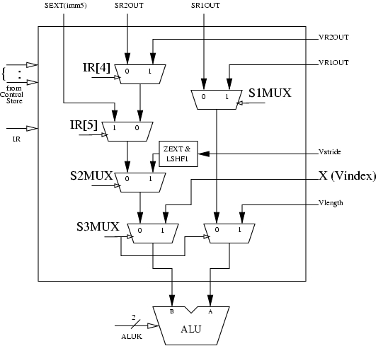
X is the Vector Index Register, which holds the pointer to the element that is being processed by the vector instruction.
-
The two control signals are RESET.VINDEX and INCREMENT.VINDEX
-
-
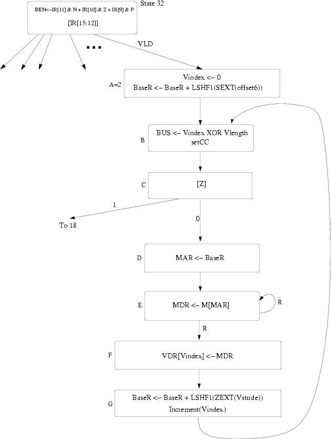
The following solution assumes a change to the microsequencer to branch according to the Z condition code.
In this problem, we assume that both of the rotators are right rotators. If the rotator for read is a right rotator and the rotator for write is a left rotator, PA[1:0] can be used as the control for both rotators.
| PA[1:0] | SIZE | RD/WR | 1st/2nd | LD.MDR[3:0] | ROT[1:0] | WE[3:0] |
|---|---|---|---|---|---|---|
| 00 | B | RD | X | XXX1 | 00 | 0000 |
| 00 | B | WR | X | XXX0 | 00 | 0001 |
| 00 | H | RD | X | XX11 | 00 | 0000 |
| 00 | H | WR | X | XX00 | 00 | 0011 |
| 00 | W | RD | X | 1111 | 00 | 0000 |
| 00 | W | WR | X | 0000 | 00 | 1111 |
| 01 | B | RD | X | XXX1 | 01 | 0000 |
| 01 | B | WR | X | XXX0 | 11 | 0010 |
| 01 | H | RD | X | XX11 | 01 | 0000 |
| 01 | H | WR | X | XX00 | 11 | 0110 |
| 01 | W | RD | 1st | X111 | 01 | 0000 |
| 01 | W | RD | 2nd | 1000 | 01 | 0000 |
| 01 | W | WR | 1st | 0000 | 11 | 1110 |
| 01 | W | WR | 2nd | 0000 | 11 | 0001 |
| 10 | B | RD | X | XXX1 | 10 | 0000 |
| 10 | B | WR | X | XXX0 | 10 | 0100 |
| 10 | H | RD | X | XX11 | 10 | 0000 |
| 10 | H | WR | X | XX00 | 10 | 1100 |
| 10 | W | RD | 1st | XX11 | 10 | 0000 |
| 10 | W | RD | 2nd | 1100 | 10 | 0000 |
| 10 | W | WR | 1st | 0000 | 10 | 1100 |
| 10 | W | WR | 2nd | 0000 | 10 | 0011 |
| 11 | B | RD | X | XXX1 | 11 | 0000 |
| 11 | B | WR | X | XXX0 | 01 | 1000 |
| 11 | H | RD | 1st | XXX1 | 11 | 0000 |
| 11 | H | RD | 2nd | XX10 | 11 | 0000 |
| 11 | H | WR | 1st | XX00 | 01 | 1000 |
| 11 | H | WR | 2nd | XX00 | 01 | 0001 |
| 11 | W | RD | 1st | XXX1 | 11 | 0000 |
| 11 | W | RD | 2nd | 1110 | 11 | 0000 |
| 11 | W | WR | 1st | 0000 | 01 | 1000 |
| 11 | W | WR | 2nd | 0000 | 01 | 0111 |
| B(yte) | 00 |
| H(alf word) | 01 |
| W(ord) | 10 |
| RD(read) | 0 |
| WR(write) | 1 |
| 1st | 0 |
| 2nd | 1 |
Interleave into 64 banks in order to hide the latency in sequential accesses (note, minimum needed is 37 banks but one would really prefer to use a power of 2, therefore 64).