Perform the following logical operations. Express your answers in hexadecimal notation.
- xABCD OR x9876
- x1234 XOR x1234
- xFEED AND (NOT(xBEEF))
A<=Has Professor Patt been uncomfortably warm this summer?
B<=Does Professor Patt want a new, fresher look?
C<=Are beards cool?
We think that Professor Patt should shave his beard if he has been uncomfortably warm this summer. He should also shave his beard if he wants a new fresher look and beards are not cool.
Write the logic equation for Y in terms of A,B,C that solves this problem, and draw the gate-level diagram.
- (3.11) Draw a transistor-level diagram for a three-input AND gate and a three-input OR gate. Do this by extending the designs from Figures 3.6a and 3.7a. (Figures can be found in the book on pages 56 & 57 respectively).
- Replace the transistors in your diagrams from part (a)
with either a wire or no wire to reflect the circuit’s operation when
the following inputs are applied:
-
A = 1, B = 0, C = 0
- The transistor circuit shown below produces the accompanying truth table. The inputs to some of the gates of the transistors are not specified. Also, the outputs for some of the input combinations of the truth table are not specified. Complete both specifications. i.e., all transistors will have their gates properly labeled with either A, B, or C,
and all rows of the truth table will have a 0 or 1 specified as the output.
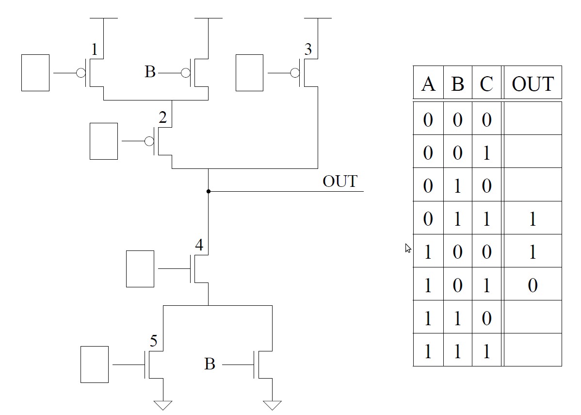
Figure 1
For example, in part a, the missing item is X. That is 0 OR 0 = 0 and 0 OR 1 = 1.
- 0 OR X = ___
- 1 OR X = ___
- 0 AND X = ___
- 1 AND X = ___
- __ XOR X = X
Logic circuit 1 in Figure 3.36 (page 87 of the book) has inputs A, B, C. Logic circuit 2 in Figure 3.37 (page 87 of the book) has inputs A and B. Both logic circuits have an output D. There is a fundamental difference between the behavioral characteristics of these two circuits. What is it? Hint: What happens when the voltage at input A goes from 0 to 1 in both circuits?
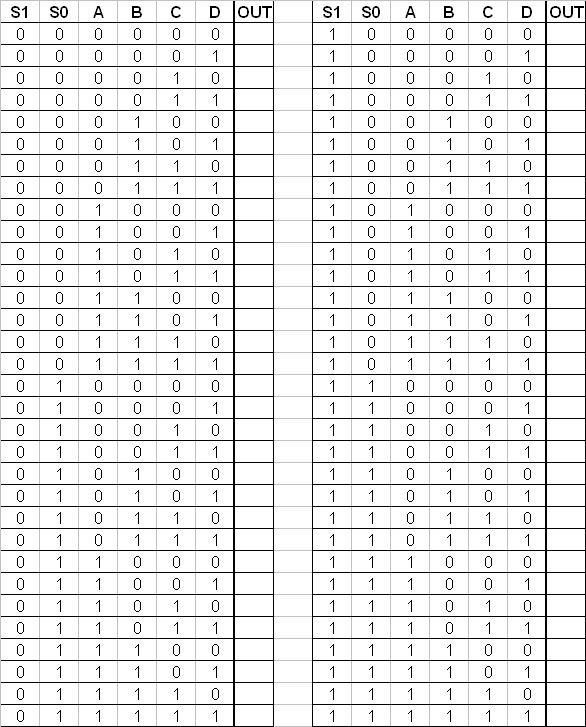
A) Implement a 4-to-1 mux using only 2-to-1 muxes making sure to properly connect all of the terminals. Remember that you will have 4 inputs (A, B, C, and D), 2 control signals (S1 and S0), and 1 output (OUT). After implementing the 4-1 mux, fill in the truth table below.
B) Implement F = A xor B using ONLY two 2-to-1 muxes. You are not allowed to use a not gate (A' and B' are not available).
Say the speed of a logic structure depends on the largest number of logic gates through which any of the inputs must propagate to reach an output. Assume that a NOT, an AND, and an OR gate all count as one gate delay. For example, the propagation delay for a two-input decoder shown in Figure 3.11 is 2 because some inputs propagate through two gates.
- What is the propagation delay for the two-input mux shown in Figure 3.12 (page 61)?
- What is the propagation delay for the 4-bit adder shown in Figure 3.16 (page 63)?
-
Can you reduce the propagation delay for the circuit shown in Figure 3
by implementing the equation in a different way? If so, how?
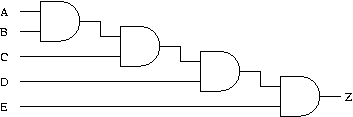
Figure 2
Recall that the adder was built with individual "slices" that produced a sum bit and carryout bit based on the two operand bits A and B and the carryin bit. We called such an element a full-adder. Suppose we have a 3-to-8 decoder and two six-input OR gates, as shown in Figure 3 below. Can we connect them so that we have a full-adder? If so, please do. (Hint: If an input to an OR gate is not needed, we can simply put an input 0 on it and it will have no effect on anything. For example, see the figure below.)
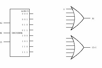
Figure 3
We wish to design a controller for an elevator such that if you push a button for a desired floor, the controller will output the floor number that the elevator should go to. However, to deter lazy people from going up or down one floor, if you push the button for the next floor (up or down), the elevator will stay on its current floor. If you push the button for the same floor that you're currently on, the controller will output the current floor number. There are four floors in the building.
Your job: construct a complete truth table for the elevator controller. It is not necessary to draw the logic here; the truth table is sufficient.
Hint: What information does the controller need in order to output the floor to go to?Hint: How many input bits will that require.
Hint: How many output bits will the controller have to supply.
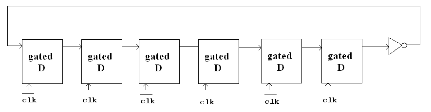
Figure 5
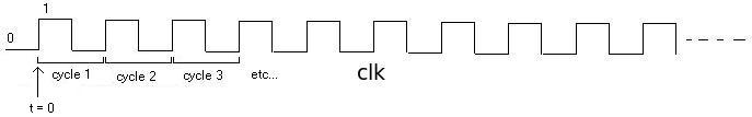
Figure 6
Question: What is the state after 50 cyles. How many cycles does it take for a specific state to show up again?
Draw the transistor level circuit of a 2 input XOR gate
A comparator circuit has two 1-bit inputs, A and B, and three 1-bit outputs, G (greater), E (equal), and L (less than). Refer to figures 3.40 and 3.41 on page 92 in the book for this problem.
- Draw the truth table
for a 1-bit comparator.
- Implement G, E and L
for a 1-bit comparator using AND, OR, and NOT gates.
- Figure
3.41 performs one-bit comparisons of the corresponding bits of two
unsigned integer A[3:0] and B[3:0]. Using the 12 one-bit results of these
4 one-bit comparators, construct a logic circuit to output a 1 if
unsigned integer A is larger than unsigned integer B (the logic circuit
should output 0 otherwise). The inputs to your logic circuit are the outputs of the
4 one-bit comparators and should be labeled G[3], E[3], L[3], G[2], E[2],
L[2], ... L[0]. (Hint: You may not need to use all 12 inputs.)
Problem added on 9/16/15
One of Professor Patt's students is always late to meetings, so Professor Patt wants you to design an alarm clock to help his student be on time. Your job is to design a logic circuit whose output Z is equal to 1 when the alarm clock should go off. The circuit will receive four input variables (A, B, C, D) that answer four different yes/no question (1=yes, 0=no):
A <= Is it going to be sunny today?
B <= Is it the weekend?
C <= Is it 7:00am?
D <= Is it 9:00am?
Professor Patt wants the alarm clock to go off if it's sunny and it's either 7:00am or 9:00am. The alarm clock should go off if it's the weekend and it's 9:00am. The alarm clock should also go off if it's not the weekend and it's 7:00am. Write the truth table and draw a gate-level diagram that performs this logic.
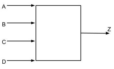
Figure 7