Chapter 12: Interrupts
Embedded
Systems - Shape The World
Modified to be compatible with EE319K Lab 6
Jonathan
Valvano and Ramesh Yerraballi
An embedded system uses its input/output devices to interact with the external world. Input devices allow the computer to gather information, and output devices can display information. Output devices also allow the computer to manipulate its environment. The tight-coupling between the computer and external world distinguishes an embedded system from a regular computer system. The challenge is under most situations the software executes much faster than the hardware. E.g., it might take the software only 1 us to ask the hardware to clear the LCD, but the hardware might take 1 ms to complete the command. During this time, the software could execute tens of thousands of instructions. Therefore, the synchronization between the executing software and its external environment is critical for the success of an embedded system. This chapter presents general concepts about interrupts, and specific details for the Cortex™-M microcontroller. We will then use periodic interrupts to cause a software task to be executed on a periodic basis. If a GPIO pin is configured as an input, it can also be armed to invoke an interrupt on falling edges, rising edges or both falling and rising edges. Using interrupts allows the software to respond quickly to changes in the external environment.
|
Learning Objectives:
|
Video 12.0. Introduction to Interrupts |

An interrupt is the automatic transfer of software execution in response to a hardware event that is asynchronous with the current software execution. This hardware event is called a trigger. The hardware event can either be a busy to ready transition in an external I/O device (like the UART input/output) or an internal event (like bus fault, memory fault, or a periodic timer). When the hardware needs service, signified by a busy to ready state transition, it will request an interrupt by setting its trigger flag. A thread is defined as the path of action of software as it executes. The execution of the interrupt service routine is called a background thread. This thread is created by the hardware interrupt request and is killed when the interrupt service routine returns from interrupt (e.g., by executing a BX LR). A new thread is created for each interrupt request. It is important to consider each individual request as a separate thread because local variables and registers used in the interrupt service routine are unique and separate from one interrupt event to the next interrupt. In a multi-threaded system, we consider the threads as cooperating to perform an overall task. Consequently we will develop ways for the threads to communicate (e.g., FIFO) and to synchronize with each other. Most embedded systems have a single common overall goal. On the other hand, general-purpose computers can have multiple unrelated functions to perform. A process is also defined as the action of software as it executes. Processes do not necessarily cooperate towards a common shared goal. Threads share access to I/O devices, system resources, and global variables, while processes have separate global variables and system resources. Processes do not share I/O devices.
|
Video 12.1a. Interrupt Basics |
Video 12.1b. Interrupt Processing - The Context Switch |
There are no standard definitions for the terms mask, enable, and arm in the professional, Computer Science, or Computer Engineering communities. Nevertheless, in this class we will adhere to the following specific meanings. To arm a device means to allow the hardware trigger to interrupt. Conversely, to disarm a device means to shut off or disconnect the hardware trigger from the interrupts. Each potential interrupting trigger has a separate arm bit. One arms a trigger if one is interested in interrupts from this source. Conversely, one disarms a trigger if one is not interested in interrupts from this source. To enable means to allow interrupts at this time. Conversely, to disable means to postpone interrupts until a later time. On the ARM Cortex-M processor there is one interrupt enable bit for the entire interrupt system. We disable interrupts if it is currently not convenient to accept interrupts. In particular, to disable interrupts we set the I bit in PRIMASK. In C, we enable and disable interrupts by calling the functions EnableInterrupts() and DisableInterrupts() respectively.
The software has dynamic control over some aspects of the interrupt request sequence. First, each potential interrupt trigger has a separate arm bit that the software can activate or deactivate. The software will set the arm bits for those devices from which it wishes to accept interrupts, and will deactivate the arm bits within those devices from which interrupts are not to be allowed. In other words it uses the arm bits to individually select which devices will and which devices will not request interrupts. For most devices there is a enable bit in the NVIC that must be set (periodic SysTick interrupts are an exception, having no NVIC enable). The third aspect that the software controls is the interrupt enable bit. Specifically, bit 0 of the special register PRIMASK is the interrupt mask bit, I. If this bit is 1 most interrupts and exceptions are not allowed, which we will define as disabled. If the bit is 0, then interrupts are allowed, which we will define as enabled. The fourth aspect is priority. The BASEPRI register prevents interrupts with lower priority interrupts, but allows higher priority interrupts. For example if the software sets the BASEPRI to 3, then requests with level 0, 1, and 2 can interrupt, while requests at levels 3 and higher will be postponed. The software can also specify the priority level of each interrupt request. If BASEPRI is zero, then the priority feature is disabled and all interrupts are allowed. The fifth aspect is the external hardware trigger. One example of a hardware trigger is the Count flag in the NVIC_ST_CTRL_R register which is set periodically by SysTick. Another example of hardware triggers are bits in the GPIO_PORTF_RIS_R register that are set on rising or falling edges of digital input pins. Five conditions must be true for an interrupt to be generated:
1)
device arm,
2) NVIC enable,
3) global enable,
4) interrupt priority level must be higher than current level
executing, and
5) hardware event trigger.
For an interrupt to occur, these five conditions must be simultaneously true but can occur in any order.
An interrupt causes the following sequence of five events. First, the current instruction is finished. Second, the execution of the currently running program is suspended, pushing eight registers on the stack (R0, R1, R2, R3, R12, LR, PC, and PSR with the R0 on top). If the floating point unit on the TM4C123 is active, an additional 18 words will be pushed on the stack representing the floating point state, making a total of 26 words. Third, the LR is set to a specific value signifying an interrupt service routine (ISR) is being run (bits [31:4] to 0xFFFFFFF, and bits [3:0] specify the type of interrupt return to perform). In our examples we will see LR is set to 0xFFFFFFF9. If the floating point registers were pushed, the LR will be 0xFFFFFFE9. Fourth, the IPSR is set to the interrupt number being processed. Lastly, the PC is loaded with the address of the ISR (vector).
1)
Current instruction is finished,
2) Eight registers are pushed on the stack,
3) LR is set to 0xFFFFFFF9,
4) IPSR is set to the interrupt number,
5) PC is loaded with the interrupt vector
These five steps, called a context switch, occur automatically in hardware as the context is switched from a foreground thread to a background thread. We can also have a context switch from a lower priority ISR to a higher priority ISR. Next, the software executes the ISR.
If a trigger flag is set, but the interrupts are disabled (I=1), the interrupt level is not high enough, or the flag is disarmed, the request is not dismissed. Rather the request is held pending, postponed until a later time, when the system deems it convenient to handle the requests. In other words, once the trigger flag is set, under most cases it remains set until the software clears it. The five necessary events (device arm, NVIC enable, global enable, level, and trigger) can occur in any order. For example, the software can set the I bit to prevent interrupts, run some code that needs to run to completion, and then clear the I bit. A trigger occurring while running with I=1 is postponed until the time the I bit is cleared again.
Clearing a trigger flag is called acknowledgement, which occurs only by specific software action. Each trigger flag has a specific action software must perform to clear that flag. We will pay special attention to these enable/disable software actions. The SysTick periodic interrupt will be the only example of an automatic acknowledgement. For SysTick, the periodic timer requests an interrupt, but the trigger flag will be automatically cleared when the ISR runs. For all the other trigger flags, the ISR must explicitly execute code that clears the flag.
The interrupt service routine (ISR) is the software module that is executed when the hardware requests an interrupt. There may be one large ISR that handles all requests (polled interrupts), or many small ISRs specific for each potential source of interrupt (vectored interrupts). The design of the interrupt service routine requires careful consideration of many factors. Except for the SysTick interrupt, the ISR software must explicitly clear the trigger flag that caused the interrupt (acknowledge). After the ISR provides the necessary service, it will execute BX LR. Because LR contains a special value (e.g., 0xFFFFFFF9), this instruction pops the 8 registers from the stack, which returns control to the main program. If the LR is 0xFFFFFFE9, then 26 registers (R0-R3,R12,LR,PC,PSW, and 18 floating point registers) will be popped by BX LR. There are two stack pointers: PSP and MSP. The software in this class will exclusively use the MSP. It is imperative that the ISR software balance the stack before exiting. Execution of the previous thread will then continue with the exact stack and register values that existed before the interrupt. Although interrupt handlers can create and use local variables, parameter passing between threads must be implemented using shared global memory variables. A private global variable can be used if an interrupt thread wishes to pass information to itself, e.g., from one interrupt instance to another. The execution of the main program is called the foreground thread, and the executions of the various interrupt service routines are called background threads.
An axiom with interrupt synchronization is that the ISR should execute as fast as possible. The interrupt should occur when it is time to perform a needed function, and the interrupt service routine should perform that function, and return right away. Placing backward branches (busy-wait loops, iterations) in the interrupt software should be avoided if possible. The percentage of time spent executing interrupt software should be small when compared to the time between interrupt triggers.
Performance measures: latency and bandwidth. For an input device, the interface latency is the time between when new input is available, and the time when the software reads the input data. We can also define device latency as the response time of the external I/O device. For example, if we request that a certain sector be read from a disk, then the device latency is the time it take to find the correct track and spin the disk (seek) so the proper sector is positioned under the read head. For an output device, the interface latency is the time between when the output device is idle, and the time when the software writes new data. A real-time system is one that can guarantee a worst case interface latency. Bandwidth is defined as the amount of data/sec being processed.
Many factors should be considered when deciding the most appropriate mechanism to synchronize hardware and software. One should not always use busy wait because one is too lazy to implement the complexities of interrupts. On the other hand, one should not always use interrupts because they are fun and exciting. Busy-wait synchronization is appropriate when the I/O timing is predictable and when the I/O structure is simple and fixed. Busy wait should be used for dedicated single thread systems where there is nothing else to do while the I/O is busy. Interrupt synchronization is appropriate when the I/O timing is variable, and when the I/O structure is complex. In particular, interrupts are efficient when there are I/O devices with different speeds. Interrupts allow for quick response times to important events. In particular, using interrupts is one mechanism to design real-time systems, where the interface latency must be short and bounded. Bounded means it is always less than a specified value. Short means the specified value is acceptable to our consumers.
Interrupts can also be used for infrequent but critical events like power failure, memory faults, and machine errors. Periodic interrupts will be useful for real-time clocks, data acquisition systems, and control systems. For extremely high bandwidth and low latency interfaces, direct memory access (DMA) should be used. DMA is described in Embedded Systems: Real-Time Operating Systems for ARM® Cortex™-M Microcontrollers . This example uses a timer and DMA to input data from an input port and store it in RAM http://users.ece.utexas.edu/~valvano/arm/DMATimer_4F120.zip and is beyond the scope of this introductory class.
An atomic operation is a sequence that once started will always finish, and cannot be interrupted. All instructions on the ARM® Cortex™-M processor are atomic except store and load multiple, STM LDM PUSH POP. If we wish to make a section of code atomic, we can run that code with I=1. In this way, interrupts will not be able to break apart the sequence. Again, requested interrupts that are triggered while I=1 are not dismissed, but simply postponed until I=0. In particular, to implement an atomic operation we will 1) save the current value of the PRIMASK, 2) disable interrupts, 3) execute the operation that needs to run atomically, and 4) restore the PRIMASK back to its previous value.
: What five conditions must be true for an interrupt to occur?
: How do you enable interrupts?
: What are the steps that occur when an interrupt is processed?
As you develop experience using interrupts, you will come to notice a few common aspects that most computers share. The following paragraphs outline three essential mechanisms that are needed to utilize interrupts. Although every computer that uses interrupts includes all three mechanisms, how the mechanisms operate will vary from one computer to another.
All interrupting systems must have the ability for the hardware to request action from computer. In general, the interrupt requests can be generated using a separate connection to the processor for each device. The TM4C microcontrollers use separate connections to request interrupts.
All interrupting systems must have the ability for the computer to determine the source. A vectored interrupt system employs separate connections for each device so that the computer can give automatic resolution. You can recognize a vectored system because each device has a separate interrupt vector address. With a polled interrupt system, the interrupt software must poll each device, looking for the device that requested the interrupt. Most interrupts on the TM4C microcontrollers are vectored, but there are some triggers that share the same vector. For these interrupts the ISR must poll to see which trigger caused the interrupt. For example, all input pins on one GPIO port can trigger an interrupt, but the trigger flags share the same vector. So if multiple pins on one GPIO port are armed, the shared ISR must poll to determine which one(s) requested service.
The third necessary component of the interface is the ability for the computer to acknowledge the interrupt. Normally there is a trigger flag in the interface that is set on the busy to ready state transition. In essence, this trigger flag is the cause of the interrupt. Acknowledging the interrupt involves clearing this flag. It is important to shut off the request, so that the computer will not mistakenly request a second (and inappropriate) interrupt service for the same condition. Except for periodic SysTick interrupts, TM4C microcontrollers use software acknowledge. So when designing an interrupting interface, it will be important to know exactly what hardware condition sets the trigger flag (and request an interrupt) and how the software will clear it (acknowledge) in the ISR.
Common Error: The system will crash if the interrupt service routine doesn’t either acknowledge or disarm the device requesting the interrupt.
Common Error: The ISR software should not disable interrupts at the beginning nor should it reenable interrupts at the end. Which interrupts are allowed to run is automatically controlled by the priority set in the NVIC.
For regular function calls we use the registers and stack to pass parameters, but interrupt threads have logically separate registers and stack. More specifically, registers are automatically saved by the processor as it switches from main program (foreground thread) to interrupt service routine (background thread). Exiting an ISR will restore the registers back to their previous values. Thus, all parameter passing must occur through global memory. One cannot pass data from the main program to the interrupt service routine using registers or the stack.
In this chapter, multi-threading means one main program (foreground thread) and multiple ISRs (background threads). An operating system allows multiple foreground threads. For more information on operating systems see Embedded Systems: Real-Time Operating Systems for ARM® Cortex™-M Microcontrollers. Synchronizing threads is a critical task affecting efficiency and effectiveness of systems using interrupts. In this section, we will present in general form three constructs to synchronize threads: binary semaphore, mailbox, and FIFO queue.
Video 12.2. Inter-Thread Communication and Synchronization
A binary semaphore is simply a shared flag, as described in Figure 12.0. There are two operations one can perform on a semaphore. Signal is the action that sets the flag. Wait is the action that checks the flag, and if the flag is set, the flag is cleared and important stuff is performed. This flag must exist as a private global variable with restricted access to only these two code pieces. In C, we add the qualifier static to a global variable to restrict access to software within the same file. In order to reduce complexity of the system, it will be important to limit the access to this flag to as few modules as possible.
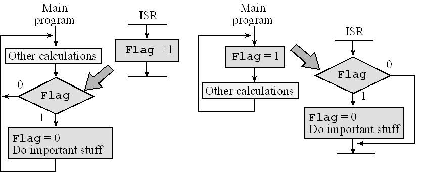
Figure 12.0. A semaphore can be used to synchronize threads.
A flag of course has two states: 0 and 1. However, it is good design to assign a meaning to this flag. For example, 0 might mean the switch has not been pressed, and 1 might mean the switch has been pressed. Figure 12.0 shows two examples of the binary semaphore. The big arrows in this figure signify synchronization links between the threads. In the example on the left, the ISR signals the semaphore and the main program waits on the semaphore. Notice the “important stuff” is run in the foreground once per execution of the ISR. In the example on the right, the main program signals the semaphore and the ISR waits. It is good design to have NO backwards jumps in an ISR. In this particular application, if the ISR is running and the semaphore is 0, the action is just skipped and the computer returns from the interrupt.
The second inter-thread synchronization scheme is the mailbox. The mailbox is a binary semaphore with associated data variable. Interactive Tool 12.1 illustrates an input device interfaced using interrupt synchronization and uses a mailbox to send data from ISR to the main program. The mailbox structure is implemented with two shared global variables. Mail contains data, and Status is a semaphore flag specifying whether the mailbox is full or empty.
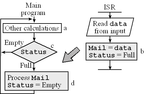
Figure 12.1. A mailbox can be used to pass data between threads.
Code Blocks, A, B, C and D refer to the blocks labelled (lower-case) in Figure 12.1. The interrupt is requested when its trigger flag is set, signifying new data are ready from the input device. The ISR will read the data from the input device and store it in the shared global variable Mail, then update its Status to full. The main program will perform other calculations, while occasionally checking the status of the mailbox. When the mailbox has data, the main program will process it. This approach is adequate for situations where the input bandwidth is slow compared to the software processing speed. One way to visualize the interrupt synchronization is to draw a state versus time plot of the activities of the hardware, the mailbox, and the two software threads .Use the following tool to how the foreground and background thread communicate using a "mailbox"
Enter 4-digit hex Data (in the format 0x****):
Using the tool demonstrates that during execution of block A, the mailbox is empty, the input device is idle and the main program is performing other tasks, because mailbox is empty. When new input data are ready, the trigger flag will be set, and an interrupt will be requested. In block B the ISR reads data from input device and saves it in Mail, and then it sets Status to full. The main program recognizes Status is full in Block C. In Block D, the main program processes data from Mail, sets Status to empty. Notice that even though there are two threads, only one is active at a time. The interrupt hardware switches the processor from the main program to the ISR, and the return from interrupt switches the processor back.
The third synchronization technique is the FIFO queue. The use of a FIFO is similar to the mailbox, but allows buffering, which is storing data in a first come first served manner. For an input device, an interrupt occurs when new input data are available, the ISR reads the data from the input device, and puts the data in the FIFO. Whenever the main program is idle, it will attempt to get data from the FIFO. If data were to exist, that data will be processed. The big arrows in Figures 12.4 and 12.5 signify the communication and synchronization link between the background and foreground.
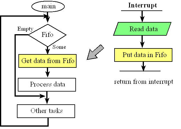
Figure 12.2. For an input device we can use a FIFO to pass data from the ISR to the main program.
For an output device, the main program puts data into the FIFO whenever it wishes to perform output. This data is buffered, and if the system is properly configured, the FIFO never becomes full and the main program never actually waits for the output to occur. An interrupt occurs when the output device is idle, the ISR gets from the FIFO and write the data to the output device. Whenever the ISR sees the FIFO is empty, it could cause the output device to become idle. The direction of the big arrows in Figures 12.2 and 12.3 signify the direction of data flow in these buffered I/O examples.
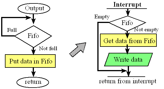
Figure 12.3. For an output device we can use a FIFO to pass data from the main program to the ISR.
There are other types of interrupt that are not an input or output. For example we will configure the computer to request an interrupt on a periodic basis. This means an interrupt handler will be executed at fixed time intervals. This periodic interrupt will be essential for the implementation of real-time data acquisition and real-time control systems. For example if we are implementing a digital controller that executes a control algorithm 100 times a second, then we will set up the internal timer hardware to request an interrupt every 10 ms. The interrupt service routine will execute the digital control algorithm and then return to the main thread. In a similar fashion, we will use periodic interrupts to perform analog input and/or analog output. For example if we wish to sample the ADC 100 times a second, then we will set up the internal timer hardware to request an interrupt every 10 ms. The interrupt service routine will sample the ADC, process (or save) the data, and then return to the main thread.
Performance Tip: It is poor design to employ backward jumps in an ISR, because they may affect the latency of other interrupt requests. Whenever you are thinking about using a backward jump, consider redesigning the system with more or different triggers to reduce the number of backward jumps.
On the ARM Cortex-M processor, exceptions include resets, software interrupts and hardware interrupts. Interrupts on the Cortex-M are controlled by the Nested Vectored Interrupt Controller (NVIC). Each exception has an associated 32-bit vector that points to the memory location where the ISR that handles the exception is located. Vectors are stored in ROM at the beginning of memory. Program 12.1 shows the first few vectors as defined in the Startup.s file. DCD is an assembler pseudo-op that defines a 32-bit constant. ROM location 0x0000.0000 has the initial stack pointer, and location 0x0000.0004 contains the initial program counter, which is called the reset vector. It points to a function called the reset handler, which is the first thing executed following reset. There are up to 240 possible interrupt sources and their 32-bit vectors are listed in order starting with location 0x0000.0008. From a programming perspective, we can attach ISRs to interrupts by writing the ISRs as regular assembly subroutines or C functions with no input or output parameters and editing the Startup.s file to specify those functions for the appropriate interrupt. For example, if we wrote a Port F interrupt service routine named PortFISR, then we would replace GPIOPortF_Handler with PortFISR. In this class, we will write our ISRs using standard function names so that the Startup.s file need not be edited. I.e., we will simply name the ISR for edge-triggered interrupts on Port F as GPIOPortF_Handler. The ISR for this interrupt is a 32-bit pointer located at ROM address 0x0000.00B8. Because the vectors are in ROM, this linkage is defined at compile time and not at run time. For more details see the Startup.s files within the interrupt examples posted on the book web site.
: Where is the vector for SysTick? What is the standard name for this ISR?
EXPORT __Vectors
__Vectors ; address ISR
DCD StackMem + Stack ; 0x00000000 Top of Stack
DCD Reset_Handler ; 0x00000004 Reset Handler
DCD NMI_Handler ; 0x00000008 NMI Handler
DCD HardFault_Handler ; 0x0000000C Hard Fault Handler
DCD MemManage_Handler ; 0x00000010 MPU Fault Handler
DCD BusFault_Handler ; 0x00000014 Bus Fault Handler
DCD UsageFault_Handler ; 0x00000018 Usage Fault Handler
DCD 0 ; 0x0000001C Reserved
DCD 0 ; 0x00000020 Reserved
DCD 0 ; 0x00000024 Reserved
DCD 0 ; 0x00000028 Reserved
DCD SVC_Handler ; 0x0000002C SVCall Handler
DCD DebugMon_Handler ; 0x00000030 Debug Monitor Handler
DCD 0 ; 0x00000034 Reserved
DCD PendSV_Handler ; 0x00000038 PendSV Handler
DCD SysTick_Handler ; 0x0000003C SysTick Handler
DCD GPIOPortA_Handler ; 0x00000040 GPIO Port A
DCD GPIOPortB_Handler ; 0x00000044 GPIO Port B
DCD GPIOPortC_Handler ; 0x00000048 GPIO Port C
DCD GPIOPortD_Handler ; 0x0000004C GPIO Port D
DCD GPIOPortE_Handler ; 0x00000050 GPIO Port E
DCD UART0_Handler ; 0x00000054 UART0
DCD UART1_Handler ; 0x00000058 UART1
DCD SSI0_Handler ; 0x0000005C SSI
DCD I2C0_Handler ; 0x00000060 I2C
DCD PWM0Fault_Handler ; 0x00000064 PWM Fault
DCD PWM0Generator0_Handler ; 0x00000068 PWM 0 Generator 0
DCD PWM0Generator1_Handler ; 0x0000006C PWM 0 Generator 1
DCD PWM0Generator2_Handler ; 0x00000070 PWM 0 Generator 2
DCD Quadrature0_Handler ; 0x00000074 Quadrature Encoder 0
DCD ADC0Seq0_Handler ; 0x00000078 ADC0 Sequence 0
DCD ADC0Seq1_Handler ; 0x0000007C ADC0 Sequence 1
DCD ADC0Seq2_Handler ; 0x00000080 ADC0 Sequence 2
DCD ADC0Seq3_Handler ; 0x00000084 ADC0 Sequence 3
DCD WDT_Handler ; 0x00000088 Watchdog
DCD Timer0A_Handler ; 0x0000008C Timer 0 subtimer A
DCD Timer0B_Handler ; 0x00000090 Timer 0 subtimer B
DCD Timer1A_Handler ; 0x00000094 Timer 1 subtimer A
DCD Timer1B_Handler ; 0x00000098 Timer 1 subtimer B
DCD Timer2A_Handler ; 0x0000009C Timer 2 subtimer A
DCD Timer2B_Handler ; 0x000000A0 Timer 2 subtimer B
DCD Comp0_Handler ; 0x000000A4 Analog Comp 0
DCD Comp1_Handler ; 0x000000A8 Analog Comp 1
DCD Comp2_Handler ; 0x000000AC Analog Comp 2
DCD SysCtl_Handler ; 0x000000B0 System Control
DCD FlashCtl_Handler ; 0x000000B4 Flash Control
DCD GPIOPortF_Handler ; 0x000000B8 GPIO Port F
Program 12.1. Software syntax to set the interrupt vectors for the TM4C (only some vectors are shown, see the startup.s file for a complete list).
Program 12.2 shows that the syntax for an ISR looks like a function with no parameters. Notice that each ISR (except for SysTick) must acknowledge the interrupt in software by clearing the flag that caused the interrupt. In Program 12.2, we assume the interrupt was caused by an edge on PF4, so writing to the ICR register will clear trigger flag 4.
void GPIOPortF_Handler(void){
GPIO_PORTF_ICR_R = 0x10; // ack, clear interrupt flag4
// stuff
}
Program 12.2. Typical interrupt service routine.
|
Vector address |
Number |
IRQ |
ISR name in Startup.s |
NVIC |
Priority bits |
|
0x00000038 |
14 |
-2 |
PendSV_Handler |
NVIC_SYS_PRI3_R |
23 – 21 |
|
0x0000003C |
15 |
-1 |
SysTick_Handler |
NVIC_SYS_PRI3_R |
31 – 29 |
|
0x00000040 |
16 |
0 |
GPIOPortA_Handler |
NVIC_PRI0_R |
7 – 5 |
|
0x00000044 |
17 |
1 |
GPIOPortB_Handler |
NVIC_PRI0_R |
15 – 13 |
|
0x00000048 |
18 |
2 |
GPIOPortC_Handler |
NVIC_PRI0_R |
23 – 21 |
|
0x0000004C |
19 |
3 |
GPIOPortD_Handler |
NVIC_PRI0_R |
31 – 29 |
|
0x00000050 |
20 |
4 |
GPIOPortE_Handler |
NVIC_PRI1_R |
7 – 5 |
|
0x00000054 |
21 |
5 |
UART0_Handler |
NVIC_PRI1_R |
15 – 13 |
|
0x00000058 |
22 |
6 |
UART1_Handler |
NVIC_PRI1_R |
23 – 21 |
|
0x0000005C |
23 |
7 |
SSI0_Handler |
NVIC_PRI1_R |
31 – 29 |
|
0x00000060 |
24 |
8 |
I2C0_Handler |
NVIC_PRI2_R |
7 – 5 |
|
0x00000064 |
25 |
9 |
PWM0Fault_Handler |
NVIC_PRI2_R |
15 – 13 |
|
0x00000068 |
26 |
10 |
PWM0_Handler |
NVIC_PRI2_R |
23 – 21 |
|
0x0000006C |
27 |
11 |
PWM1_Handler |
NVIC_PRI2_R |
31 – 29 |
|
0x00000070 |
28 |
12 |
PWM2_Handler |
NVIC_PRI3_R |
7 – 5 |
|
0x00000074 |
29 |
13 |
Quadrature0_Handler |
NVIC_PRI3_R |
15 – 13 |
|
0x00000078 |
30 |
14 |
ADC0_Handler |
NVIC_PRI3_R |
23 – 21 |
|
0x0000007C |
31 |
15 |
ADC1_Handler |
NVIC_PRI3_R |
31 – 29 |
|
0x00000080 |
32 |
16 |
ADC2_Handler |
NVIC_PRI4_R |
7 – 5 |
|
0x00000084 |
33 |
17 |
ADC3_Handler |
NVIC_PRI4_R |
15 – 13 |
|
0x00000088 |
34 |
18 |
WDT_Handler |
NVIC_PRI4_R |
23 – 21 |
|
0x0000008C |
35 |
19 |
Timer0A_Handler |
NVIC_PRI4_R |
31 – 29 |
|
0x00000090 |
36 |
20 |
Timer0B_Handler |
NVIC_PRI5_R |
7 – 5 |
|
0x00000094 |
37 |
21 |
Timer1A_Handler |
NVIC_PRI5_R |
15 – 13 |
|
0x00000098 |
38 |
22 |
Timer1B_Handler |
NVIC_PRI5_R |
23 – 21 |
|
0x0000009C |
39 |
23 |
Timer2A_Handler |
NVIC_PRI5_R |
31 – 29 |
|
0x000000A0 |
40 |
24 |
Timer2B_Handler |
NVIC_PRI6_R |
7 – 5 |
|
0x000000A4 |
41 |
25 |
Comp0_Handler |
NVIC_PRI6_R |
15 – 13 |
|
0x000000A8 |
42 |
26 |
Comp1_Handler |
NVIC_PRI6_R |
23 – 21 |
|
0x000000AC |
43 |
27 |
Comp2_Handler |
NVIC_PRI6_R |
31 – 29 |
|
0x000000B0 |
44 |
28 |
SysCtl_Handler |
NVIC_PRI7_R |
7 – 5 |
|
0x000000B4 |
45 |
29 |
FlashCtl_Handler |
NVIC_PRI7_R |
15 – 13 |
|
0x000000B8 |
46 |
30 |
GPIOPortF_Handler |
NVIC_PRI7_R |
23 – 21 |
|
0x000000BC |
47 |
31 |
GPIOPortG_Handler |
NVIC_PRI7_R |
31 – 29 |
|
0x000000C0 |
48 |
32 |
GPIOPortH_Handler |
NVIC_PRI8_R |
7 – 5 |
|
0x000000C4 |
49 |
33 |
UART2_Handler |
NVIC_PRI8_R |
15 – 13 |
|
0x000000C8 |
50 |
34 |
SSI1_Handler |
NVIC_PRI8_R |
23 – 21 |
|
0x000000CC |
51 |
35 |
Timer3A_Handler |
NVIC_PRI8_R |
31 – 29 |
|
0x000000D0 |
52 |
36 |
Timer3B_Handler |
NVIC_PRI9_R |
7 – 5 |
|
0x000000D4 |
53 |
37 |
I2C1_Handler |
NVIC_PRI9_R |
15 – 13 |
|
0x000000D8 |
54 |
38 |
Quadrature1_Handler |
NVIC_PRI9_R |
23 – 21 |
|
0x000000DC |
55 |
39 |
CAN0_Handler |
NVIC_PRI9_R |
31 – 29 |
|
0x000000E0 |
56 |
40 |
CAN1_Handler |
NVIC_PRI10_R |
7 – 5 |
|
0x000000E4 |
57 |
41 |
CAN2_Handler |
NVIC_PRI10_R |
15 – 13 |
|
0x000000E8 |
58 |
42 |
Ethernet_Handler |
NVIC_PRI10_R |
23 – 21 |
|
0x000000EC |
59 |
43 |
Hibernate_Handler |
NVIC_PRI10_R |
31 – 29 |
|
0x000000F0 |
60 |
44 |
USB0_Handler |
NVIC_PRI11_R |
7 – 5 |
|
0x000000F4 |
61 |
45 |
PWM3_Handler |
NVIC_PRI11_R |
15 – 13 |
|
0x000000F8 |
62 |
46 |
uDMA_Handler |
NVIC_PRI11_R |
23 – 21 |
|
0x000000FC |
63 |
47 |
uDMA_Error |
NVIC_PRI11_R |
31 – 29 |
Table 12.1. Some of the interrupt vectors for the TM4C. The TM4C123 has over 100 possible interrupt sources.
To activate an interrupt source we need to set its priority and enable that source in the NVIC. This activation is in addition to the arm and enable steps. Table 12.1 lists some of the interrupt sources available on the TM4C family of microcontrollers. Interrupt numbers 0 to 15 contain the faults, software interrupt and SysTick; these interrupts will be handled differently from interrupts 16 and up.
Table 12.2 shows some of the priority registers on the NVIC. Each register contains an 8-bit priority field for four devices. On the TM4C microcontrollers, only the top three bits of the 8-bit field are used. This allows us to specify the interrupt priority level for each device from 0 to 7, with 0 being the highest priority. The interrupt number (number column in Table 12.1) is loaded into the IPSR register. The servicing of interrupts does not set the I bit in the PRIMASK, so a higher priority interrupt can suspend the execution of a lower priority ISR. If a request of equal or lower priority is generated while an ISR is being executed, that request is postponed until the ISR is completed. In particular, those devices that need prompt service should be given high priority.
|
Address |
31 – 29 |
23 – 21 |
15 – 13 |
7 – 5 |
Name |
|
0xE000E400 |
GPIO Port D |
GPIO Port C |
GPIO Port B |
GPIO Port A |
NVIC_PRI0_R |
|
0xE000E404 |
SSI0, Rx Tx |
UART1, Rx Tx |
UART0, Rx Tx |
GPIO Port E |
NVIC_PRI1_R |
|
0xE000E408 |
PWM Gen 1 |
PWM Gen 0 |
PWM Fault |
I2C0 |
NVIC_PRI2_R |
|
0xE000E40C |
ADC Seq 1 |
ADC Seq 0 |
Quad Encoder |
PWM Gen 2 |
NVIC_PRI3_R |
|
0xE000E410 |
Timer 0A |
Watchdog |
ADC Seq 3 |
ADC Seq 2 |
NVIC_PRI4_R |
|
0xE000E414 |
Timer 2A |
Timer 1B |
Timer 1A |
Timer 0B |
NVIC_PRI5_R |
|
0xE000E418 |
Comp 2 |
Comp 1 |
Comp 0 |
Timer 2B |
NVIC_PRI6_R |
|
0xE000E41C |
GPIO Port G |
GPIO Port F |
Flash Control |
System Control |
NVIC_PRI7_R |
|
0xE000E420 |
Timer 3A |
SSI1, Rx Tx |
UART2, Rx Tx |
GPIO Port H |
NVIC_PRI8_R |
|
0xE000E424 |
CAN0 |
Quad Encoder 1 |
I2C1 |
Timer 3B |
NVIC_PRI9_R |
|
0xE000E428 |
Hibernate |
Ethernet |
CAN2 |
CAN1 |
NVIC_PRI10_R |
|
0xE000E42C |
uDMA Error |
uDMA Soft Tfr |
PWM Gen 3 |
USB0 |
NVIC_PRI11_R |
|
0xE000ED20 |
SysTick |
PendSV |
-- |
Debug |
NVIC_SYS_PRI3_R |
Table 12.2. The LM3S/TM4C NVIC registers. Each register is 32 bits wide. Bits not shown are zero.
There are five enable registers NVIC_EN0_R through NVIC_EN4_R. The 32 bits in register NVIC_EN0_R control the IRQ numbers 0 to 31 (interrupt numbers 16 – 47). In Table 12.1 we see UART0 is IRQ=5. To enable UART0 interrupts we set bit 5 in NVIC_EN0_R, see Table 12.3. The 32 bits in NVIC_EN1_R control the IRQ numbers 32 to 63 (interrupt numbers 48 – 79). In Table 12.1 we see UART2 is IRQ=33. To enable UART interrupts we set bit 1 (33-32=1) in NVIC_EN1_R, see Table 12.3. Not every interrupt source is available on every TM4C microcontroller, so you will need to refer to the data sheet for your microcontroller when designing I/O interfaces. Writing zeros to the NVIC_EN0_R through NVIC_EN4_R registers has no effect. To disable interrupts we write ones to the corresponding bit in the NVIC_DIS0_R through NVIC_DIS4_R register.
|
Address |
31 |
30 |
29-7 |
6 |
5 |
4 |
3 |
2 |
1 |
0 |
Name |
|
0xE000E100 |
G |
F |
… |
UART1 |
UART0 |
E |
D |
C |
B |
A |
NVIC_EN0_R |
|
0xE000E104 |
|
|
… |
|
|
|
|
|
UART2 |
H |
NVIC_EN1_R |
Table 12.3. Some of the TM4C NVIC interrupt enable registers. There are five such registers defining 139 interrupt enable bits.
Interactive tool 12.2 shows the context switch from executing in the foreground to running a periodic SysTick ISR. Before the interrupt occurs, the I bit in the PRIMASK is 0 signifying interrupts are enabled, and the interrupt number (ISRNUM) in the IPSR register is 0, meaning we are running in Thread mode (i.e., the main program, and not an ISR). Handler mode is signified by a nonzero value in IPSR. When BASEPRI register is zero, all interrupts are allowed and the BASEPRI register is not active.
When the SysTick counter goes from 1 to 0, the Count flag in the NVIC_ST_CTRL_R register is set, triggering an interrupt. The current instruction is finished. (a) Eight registers are pushed on the stack with R0 on top. These registers are pushed onto the stack . (b) The vector address is loaded into the PC (“Vector address” column in Table 12.1). (c) The IPSR register is set to 15 (“Number” column in Table 12.1) (d) The top 24 bits of LR are set to 0xFFFFFF, signifying the processor is executing an ISR. The bottom eight bits specify how to return from interrupt.
0xE1 Return to Handler mode MSP (using floating point state on TM4C)
0xE9 Return to Thread mode MSP (using floating point state on TM4C)
0xED Return to Thread mode PSP (using floating point state on TM4C)
0xF1 Return to Handler mode MSP
0xF9 Return to Thread mode MSP ← in this class we will always be using this one
0xFD Return to Thread mode PSP
After pushing the registers, the processor always uses the main stack pointer (MSP) during the execution of the ISR. Events 2, 3, and 4 can occur simultaneously
Use the following tool to see the steps involved in a context switch from the executing the foreground thread to switching to the background thread (ISR) when the Systick interrupt occurs.
Click Start to start the context switch by pushing the current registers into the stack.
To return from an interrupt, the ISR executes the typical function return BX LR. However, since the top 24 bits of LR are 0xFFFFFF, it knows to return from interrupt by popping the eight registers off the stack. Since the bottom eight bits of LR in this case are 0b11111001, it returns to thread mode using the MSP as its stack pointer. Since the IPSR is part of the PSR that is popped, it is automatically reset its previous state.
A nested interrupt occurs when a higher priority interrupt suspends an ISR. The lower priority interrupt will finish after the higher priority ISR completes. When one interrupt preempts another, the LR is set to 0xFFFFFFF1, so it knows to return to handler mode. Tail chaining occurs when one ISR executes immediately after another. Optimization occurs because the eight registers need not be popped only to be pushed once again. If an interrupt is triggered and is in the process of stacking registers when a higher priority interrupt is requested, this late arrival interrupt will be executed first.
Priority determines the order of service when two or more requests are made simultaneously. Priority also allows a higher priority request to suspend a lower priority request currently being processed. Usually, if two requests have the same priority, we do not allow them to interrupt each other. NVIC assigns a priority level to each interrupt trigger. This mechanism allows a higher priority trigger to interrupt the ISR of a lower priority request. Conversely, if a lower priority request occurs while running an ISR of a higher priority trigger, it will be postponed until the higher priority service is complete.
Observation: There are many interrupt sources, but an effective system will use only a few.
Program 12.3 gives the definitions in startup.s that allow the software to enable and disable interrupts. These functions are callable from either assembly or C code. The wait for interrupt can be used to place the processor in low-power sleep mode while it waits for an interrupt.
;*********** DisableInterrupts ***************
; disable interrupts
; inputs: none
; outputs: none
DisableInterrupts CPSID I ;set I=1
BX LR
;*********** EnableInterrupts ***************
; enable interrupts
; inputs: none
; outputs: none
EnableInterrupts CPSIE I ;set I=0
BX LR
;*********** WaitForInterrupt ************************
; go to low power mode while waiting for the next interrupt
; inputs: none
; outputs: none
WaitForInterrupt
WFI
BX LR
Program 12.3. Assembly functions needed for interrupt enabling and disabling.
|
Video 12.3a. Edge-Trigerred Interrupt |
Video 12.3b. Edge-Trigerred Interrupt Configuration |
Synchronizing software to hardware events requires the software to recognize when the hardware changes states from busy to done. Many times the busy to done state transition is signified by a rising (or falling) edge on a status signal in the hardware. For these situations, we connect this status signal to an input of the microcontroller, and we use edge-triggered interfacing to configure the interface to set a flag on the rising (or falling) edge of the input. Using edge-triggered interfacing allows the software to respond quickly to changes in the external world. If we are using busy-wait synchronization, the software waits for the flag. If we are using interrupt synchronization, we configure the flag to request an interrupt when set. Each of the digital I/O pins on the TM4C family can be configured for edge triggering. Table 12.4 shows the registers needed to set up edge triggering for Port A. The differences between members of the TM4C family include the number of ports (e.g., the TM4C123 has ports A – F) and the number of pins in each port (e.g., the TM4C123 only has pins 4 – 0 in Port F). For more details, refer to the datasheet for your specific microcontroller. Any or all of digital I/O pins can be configured as an edge-triggered input. When writing C code using these registers, include the header file for your particular microcontroller (e.g., tm4c123ge6pm.h). To use any of the features for a digital I/O port, we first enable its clock in the Run Mode Clock Gating Control Register (RCGCGPIO). For each bit we wish to use we must set the corresponding DEN (Digital Enable) bit. To use edge triggered interrupts we will clear the corresponding bits in the PCTL register, and we will clear bits in the AFSEL (Alternate Function Select) register. We clear DIR (Direction) bits to make them input. On the TM4C123, only pins PD7 and PF0 need to be unlocked. We clear bits in the AMSEL register to disable analog function.
|
Address |
7 |
6 |
5 |
4 |
3 |
2 |
1 |
0 |
Name |
|
$4000.43FC |
DATA |
DATA |
DATA |
DATA |
DATA |
DATA |
DATA |
DATA |
GPIO_PORTA_DATA_R |
|
$4000.4400 |
DIR |
DIR |
DIR |
DIR |
DIR |
DIR |
DIR |
DIR |
GPIO_PORTA_DIR_R |
|
$4000.4404 |
IS |
IS |
IS |
IS |
IS |
IS |
IS |
IS |
GPIO_PORTA_IS_R |
|
$4000.4408 |
IBE |
IBE |
IBE |
IBE |
IBE |
IBE |
IBE |
IBE |
GPIO_PORTA_IBE_R |
|
$4000.440C |
IEV |
IEV |
IEV |
IEV |
IEV |
IEV |
IEV |
IEV |
GPIO_PORTA_IEV_R |
|
$4000.4410 |
IME |
IME |
IME |
IME |
IME |
IME |
IME |
IME |
GPIO_PORTA_IM_R |
|
$4000.4414 |
RIS |
RIS |
RIS |
RIS |
RIS |
RIS |
RIS |
RIS |
GPIO_PORTA_RIS_R |
|
$4000.4418 |
MIS |
MIS |
MIS |
MIS |
MIS |
MIS |
MIS |
MIS |
GPIO_PORTA_MIS_R |
|
$4000.441C |
ICR |
ICR |
ICR |
ICR |
ICR |
ICR |
ICR |
ICR |
GPIO_PORTA_ICR_R |
|
$4000.4420 |
SEL |
SEL |
SEL |
SEL |
SEL |
SEL |
SEL |
SEL |
GPIO_PORTA_AFSEL_R |
|
$4000.4500 |
DRV2 |
DRV2 |
DRV2 |
DRV2 |
DRV2 |
DRV2 |
DRV2 |
DRV2 |
GPIO_PORTA_DR2R_R |
|
$4000.4504 |
DRV4 |
DRV4 |
DRV4 |
DRV4 |
DRV4 |
DRV4 |
DRV4 |
DRV4 |
GPIO_PORTA_DR4R_R |
|
$4000.4508 |
DRV8 |
DRV8 |
DRV8 |
DRV8 |
DRV8 |
DRV8 |
DRV8 |
DRV8 |
GPIO_PORTA_DR8R_R |
|
$4000.450C |
ODE |
ODE |
ODE |
ODE |
ODE |
ODE |
ODE |
ODE |
GPIO_PORTA_ODR_R |
|
$4000.4510 |
PUE |
PUE |
PUE |
PUE |
PUE |
PUE |
PUE |
PUE |
GPIO_PORTA_PUR_R |
|
$4000.4514 |
PDE |
PDE |
PDE |
PDE |
PDE |
PDE |
PDE |
PDE |
GPIO_PORTA_PDR_R |
|
$4000.4518 |
SLR |
SLR |
SLR |
SLR |
SLR |
SLR |
SLR |
SLR |
GPIO_PORTA_SLR_R |
|
$4000.451C |
DEN |
DEN |
DEN |
DEN |
DEN |
DEN |
DEN |
DEN |
GPIO_PORTA_DEN_R |
|
$4000.4524 |
CR |
CR |
CR |
CR |
CR |
CR |
CR |
CR |
GPIO_PORTA_CR_R |
|
$4000.4528 |
AMSEL |
AMSEL |
AMSEL |
AMSEL |
AMSEL |
AMSEL |
AMSEL |
AMSEL |
GPIO_PORTA_AMSEL_R |
|
|
|
|
|
|
|
|
|
|
|
|
|
31-28 |
27-24 |
23-20 |
19-16 |
15-12 |
11-8 |
7-4 |
3-0 |
|
|
$4000.452C |
PMC7 |
PMC6 |
PMC5 |
PMC4 |
PMC3 |
PMC2 |
PMC1 |
PMC0 |
GPIO_PORTA_PCTL_R |
|
$4000.4520 |
LOCK (32 bits) |
GPIO_PORTA_LOCK_R |
|||||||
Table 12.4. Some TM4C port A registers. We will clear PMC bits to used edge triggered interrupts.
To configure an edge-triggered pin, we first enable the clock on the port and configure the pin as a regular digital input. Clearing the IS (Interrupt Sense) bit configures the bit for edge triggering. If the IS bit were to be set, the trigger occurs on the level of the pin. Since most busy to done conditions are signified by edges, we typically trigger on edges rather than levels. Next we write to the IBE (Interrupt Both Edges) and IEV (Interrupt Event) bits to define the active edge. We can trigger on the rising, falling, or both edges, as listed in Table 12.5.
The hardware sets an RIS (Raw Interrupt Status) bit (called the trigger) and the software clears it (called the acknowledgement). The triggering event listed in Table 12.5 will set the corresponding RIS bit in the GPIO_PORTA_RIS_R register regardless of whether or not that bit is allowed to request an interrupt. In other words, clearing an IM bit disables the corresponding pin’s interrupt, but it will still set the corresponding RIS bit when the interrupt would have occurred. The software can acknowledge the event by writing ones to the corresponding IC (Interrupt Clear) bit in the GPIO_PORTA_IC_R register. The RIS bits are read only, meaning if the software were to write to this register, it would have no effect. For example, to clear bits 2, 1, and 0 in the GPIO_PORTA_RIS_R register, we write a 0x07 to the GPIO_PORTA_IC_R register. Writing zeros into IC bits will not affect the RIS bits.
|
DIR |
AFSEL |
PMC |
IS |
IBE |
IEV |
IME |
Port mode |
|
0 |
0 |
0000 |
0 |
0 |
0 |
0 |
Input, falling edge trigger, busy wait |
|
0 |
0 |
0000 |
0 |
0 |
1 |
0 |
Input, rising edge trigger, busy wait |
|
0 |
0 |
0000 |
0 |
1 |
- |
0 |
Input, both edges trigger, busy wait |
|
0 |
0 |
0000 |
0 |
0 |
0 |
1 |
Input, falling edge trigger, interrupt |
|
0 |
0 |
0000 |
0 |
0 |
1 |
1 |
Input, rising edge trigger, interrupt |
|
0 |
0 |
0000 |
0 |
1 |
- |
1 |
Input, both edges trigger, interrupt |
Table 12.5. Edge-triggered modes.
For input signals we have the option of adding either a pull-up resistor or a pull-down resistor. If we set the corresponding PUE (Pull-Up Enable) bit on an input pin, the equivalent of a 13 kΩ to 30 kΩ resistor to +3.3 V power is internally connected to the pin. Similarly, if we set the corresponding PDE (Pull-Down Enable) bit on an input pin, the equivalent of a 13 kΩ to 35 kΩ resistor to ground is internally connected to the pin. We cannot have both pull-up and a pull-down resistor, so setting a bit in one register automatically clears the corresponding bit in the other register.
A typical application of pull-up and pull-down mode is the interface of simple switches. Using these modes eliminates the need for an external resistor when interfacing a switch. Compare the interfaces on Port A to the interfaces on Port B illustrated in Figure 12.4. The PA2 and PA3 interfaces will use software-configured internal resistors, while the PB2 and PB3 interfaces use actual resistors. The PA2 and PB2 interfaces in Figure 12.4a) implement negative logic switch inputs, and the PA3 and PB3 interfaces in Figure 12.4b) implement positive logic switch inputs.
: What do negative logic and positive logic mean in this context?
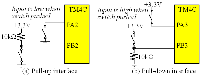
Figure 12.4. Edge-triggered interfaces can generate interrupts on a switch touch.
Using edge triggering to synchronize software to hardware centers around the operation of the trigger flags, RIS. A busy-wait interface will read the appropriate RIS bit over and over, until it is set. When the RIS bit is set, the software will clear the RIS bit (by writing a one to the corresponding IC bit) and perform the desired function. With interrupt synchronization, the initialization phase will arm the trigger flag by setting the corresponding IM bit. In this way, the active edge of the pin will set the RIS and request an interrupt. The interrupt will suspend the main program and run a special interrupt service routine (ISR). This ISR will clear the RIS bit and perform the desired function. At the end of the ISR it will return, causing the main program to resume. In particular, five conditions must be simultaneously true for an edge-triggered interrupt to be requested:
• The trigger flag bit is set (RIS)
• The arm bit is set (IME)
• The level of the edge-triggered interrupt must be less than BASEPRI
• The edge-triggered interrupt must be enabled in the NVIC_EN0_R
• The I bit, bit 0 of the special register PRIMASK, is 0
: What values to you write into DIR, AFSEL, PUE, and PDE to configure the switch interfaces of PA2 and PA3 in Figure 12.4?
Table 12.4 listed the registers for Port A. The other ports have similar registers. We will begin with a simple example that counts the number of rising edges on Port F bit 4 (Program 12.4). The initialization requires many steps. (a) The clock for the port must be enabled. (b) The global variables should be initialized. (c) The appropriate pins must be enabled as inputs. (d) We must specify whether to trigger on the rise, the fall, or both edges. In this case we will trigger on the rise of PF4. (e) It is good design to clear the trigger flag during initialization so that the first interrupt occurs due to the first rising edge after the initialization has been run. We do not wish to count a rising edge that might have occurred during the power up phase of the system. (f) We arm the edge-trigger by setting the corresponding bits in the IM register. (g) We establish the priority of Port F by setting bits 23 – 21 in the NVIC_PRI7_R register as listed in Table 9.2. We activate Port F interrupts in the NVIC by setting bit 30 in the NVIC_EN0_R register, Table 12.3. There is no need to unlock PF4.
|
volatile uint32_t FallingEdges = 0; void EdgeCounter_Init(void){ SYSCTL_RCGCGPIO_R |= 0x00000020; // (a) activate clock for port F
FallingEdges =
0;
// (b) initialize count and wait for clock GPIO_PORTF_DEN_R |= 0x10; // enable digital I/O on PF4 GPIO_PORTF_PUR_R |= 0x10; // enable weak pull-up on PF4 GPIO_PORTF_IS_R &= ~0x10; // (d) PF4 is edge-sensitive GPIO_PORTF_IBE_R &= ~0x10; // PF4 is not both edges GPIO_PORTF_IEV_R &= ~0x10; // PF4 falling edge event GPIO_PORTF_ICR_R = 0x10; // (e) clear flag4 GPIO_PORTF_IM_R |= 0x10; // (f) arm interrupt on PF4 NVIC_PRI7_R = (NVIC_PRI7_R&0xFF00FFFF)|0x00A00000; // (g) priority 5 NVIC_EN0_R = 0x40000000; // (h) enable interrupt 30 in NVIC EnableInterrupts(); // (i) Enable global Interrupt flag (I) } void GPIOPortF_Handler(void){ GPIO_PORTF_ICR_R = 0x10; // acknowledge flag4 FallingEdges = FallingEdges + 1; } int main(void){ Program 12.4. Interrupt-driven edge-triggered input that counts rising edges of PF4 (C12_EdgeInterrupt). |
Video 12.3c. EdgeInterrupt example Code Demo |
This initialization is shown to enable interrupts in step (i). However, in most systems we would not enable interrupts in the device initialization. Rather, it is good design to initialize all devices in the system, then enable interrupts. All ISRs must acknowledge the interrupt by clearing the trigger flag that requested the interrupt. For edge-triggered PF4, the trigger flag is bit 4 of the GPIO_PORTF_RIS_R register. This flag can be cleared by writing a 0x10 to GPIO_PORTF_ICR_R.
If two or more triggers share the same vector, these requests are called polled interrupts, and the ISR must determine which trigger generated the interrupt. If the requests have separate vectors, then these requests are called vectored interrupts and the ISR knows which trigger caused the interrupt.
One of the problems with switches is called switch bounce. Many inexpensive switches will mechanically oscillate for up to a few milliseconds when touched or released. It behaves like an underdamped oscillator. These mechanical oscillations cause electrical oscillations such that a port pin will oscillate high/low during the bounce. In some cases this bounce should be removed. To remove switch bounce we can ignore changes in a switch that occur within 10 ms of each other. In other words, recognize a switch transition, disarm interrupts for 10ms, and then rearm after 10 ms. Alternatively, we could record the time of the switch transition. If the time between this transition and the previous transition is less than 10ms, ignore it. If the time is more than 10 ms, then accept and process the input as a real event.
One application of periodic interrupts is called “intermittent polling” or “periodic polling”. Figure 12.5 shows busy wait side by side with periodic polling. In busy-wait synchronization, the main program polls the I/O devices continuously. With periodic polling, the I/O devices are polled on a regular basis (established by the periodic interrupt.) If no device needs service, then the interrupt simply returns.
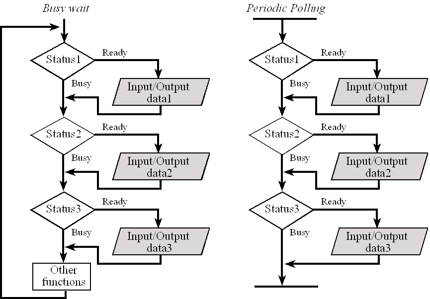
Figure 12.5. On the left is busy-wait, and on the right is periodic polling.
If the polling period is Δt, then on average the interface latency will be ½Δt, and the worst case latency will be Δt. Periodic polling is appropriate for low bandwidth devices where real-time response is not necessary. This method frees the main program to perform other functions. We use periodic polling if the following two conditions apply:
1. The I/O hardware cannot generate interrupts directly
2. We wish to perform the I/O functions in the background
For a data acquisition system, it is important to establish an accurate sampling rate. The time in between ADC samples must be equal and known in order for the digital signal processing to function properly. Similarly for microcontroller-based control systems, it is important to maintain a periodic rate for reading data from the sensors and outputing commands to the actuators.
The SysTick timer is a simple way to create periodic interrupts. A periodic interrupt is one that is requested on a fixed time basis. This interfacing technique is required for data acquisition and control systems, because software servicing must be performed at accurate time intervals.
Table 12.6 shows the SysTick registers used to create a periodic interrupt. SysTick has a 24-bit counter that decrements at the bus clock frequency. Let fBUS be the frequency of the bus clock, and let n be the value of the RELOAD register. The frequency of the periodic interrupt will be fBUS/(n+1). First, we clear the ENABLE bit to turn off SysTick during initialization. Second, we set the RELOAD register. Third, we write any value to NVIC_ST_CURRENT_R to clear the counter. Lastly, we write the desired mode to the control register, NVIC_ST_CTRL_R. We must set CLK_SRC=1, because CLK_SRC=0 external clock mode is not implemented on the LM3S/TM4C family. We set INTEN to enable interrupts. We establish the priority of the SysTick interrupts using the TICK field in the NVIC_SYS_PRI3_R register. We need to set the ENABLE bit so the counter will run. When the CURRENT value counts down from 1 to 0, the COUNT flag is set. On the next clock, the CURRENT is loaded with the RELOAD value. In this way, the SysTick counter (CURRENT) is continuously decrementing. If the RELOAD value is n, then the SysTick counter operates at modulo n+1 (…n, n-1, n-2 … 1, 0, n, n-1, …). In other words, it rolls over every n+1 counts. Thus, the COUNT flag will be set every n+1 counts. Program 12.5 shows a simple example of SysTick. SysTick is the only interrupt on the TM4C that has an automatic acknowledge. Notice there is no explicit software step in the ISR to clear the COUNT flag.
|
Address |
31-24 |
23-17 |
16 |
15-3 |
2 |
1 |
0 |
Name |
|
$E000E010 |
0 |
0 |
COUNT |
0 |
CLK_SRC |
INTEN |
ENABLE |
NVIC_ST_CTRL_R |
|
$E000E014 |
0 |
24-bit RELOAD value |
NVIC_ST_RELOAD_R |
|||||
|
$E000E018 |
0 |
24-bit CURRENT value of SysTick counter |
NVIC_ST_CURRENT_R |
|||||
|
Address |
31-29 |
28-24 |
23-21 |
20-8 |
7-5 |
4-0 |
Name |
|
$E000ED20 |
TICK |
0 |
PENDSV |
0 |
DEBUG |
0 |
NVIC_SYS_PRI3_R |
Table 12.6. SysTick registers.
|
volatile uint32_t Counts=0; void SysTick_Init(uint32_t period){ NVIC_ST_CTRL_R = 0; // disable SysTick during setup NVIC_ST_RELOAD_R = period-1;// reload value NVIC_ST_CURRENT_R = 0; // any write to current clears it NVIC_SYS_PRI3_R = (NVIC_SYS_PRI3_R&0x00FFFFFF)|0x40000000; // priority 2 NVIC_ST_CTRL_R = 0x07; // enable SysTick with core clock and interrupts // enable interrupts after all initialization is finished } void SysTick_Handler(void){ GPIO_PORTF_DATA_R ^= 0x04; // toggle PF2 Counts = Counts + 1; } int
main(void){ // running at 16 MHz Program 12.5 Implementation of a periodic interrupt using SysTick (C12_PeriodicSysTickInts). |
Video 12.3d. PeriodicSysTickInts Code Demo |
Example 12.1. Design an interface 32 Ω speaker and use it to generate a soft 1 kHz sound.
Solution: To make sound we need to create an oscillating wave. In this example, the wave will be a simple square wave. At 3.3V, a 32 Ω speaker will require a current of about 100 mA. The maximum the TM4C123 can produce on an output pin is 8 mA. If we place a resistor in series with the head phones, then the current will only be 3.3V/(1500+32Ω) = 2.2mA. To generate the 1 kHz sound we need a 1 kHz square wave. There are many good methods to generate square waves. In this example we will implement one of the simplest methods: period interrupt and toggle an output pin in the ISR. To generate a 1 kHz wave we will toggle the PA5 pin every 500 µs. We will assume the PLL is active and the system is running at 80 MHz. We wish to initialize the SysTick to interrupt with a period of 500 µs. The correct value for reload is 39999 ((500µs/12.5ns)-1). If the bus frequency were to be 16 MHz, we would set the reload value to be 7999 ((500µs/62.5ns)-1). Since this sound wave output is a real time signal, we set its priority to highest level, which is 0. See Program 12.6.
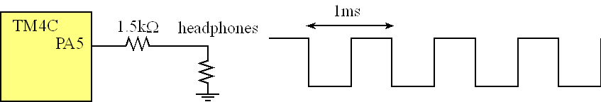
Figure 12.6. A squarewave output connected to a speaker will generate sound.
void Sound_Init(void){ uint32_t volatile delay;
SYSCTL_RCGCGPIO_R |= 0x00000001; // activate port A
delay = SYSCTL_RCGCGPIO_R;
GPIO_PORTA_DIR_R |= 0x20; // make PA5 out
GPIO_PORTA_DR8R_R |= 0x20; // can drive up to 8mA out
GPIO_PORTA_DEN_R |= 0x20; // enable digital I/O on PA5
NVIC_ST_CTRL_R = 0; // disable SysTick during setup
NVIC_ST_RELOAD_R = 39999; // reload value for 500us (assuming 80MHz)
NVIC_ST_CURRENT_R = 0; // any write to current clears it
NVIC_SYS_PRI3_R = NVIC_SYS_PRI3_R&0x00FFFFFF; // priority 0
NVIC_ST_CTRL_R = 0x00000007; // enable with core clock and interrupts
EnableInterrupts();
}
void SysTick_Handler(void){
GPIO_PORTA_DATA_R ^= 0x20; // toggle PA5
}
Program 12.6. Sound output using a periodic interrupt (C12_SoftSound).
Observation: To make a quieter sound, we could use a larger resistor between the PA5 output and the speaker.
The DC motor has a frame that remains motionless (called the stator), and an armature that moves (called the rotor). A brushed DC motor has an electromagnetic coil as well, located on the rotor, and the rotor is positioned inside the stator. In Figure 12.7, North and South refer to a permanent magnet, generating a constant B field from left to right. In this case, the rotor moves in a circular manner. When current flows through the coil, a magnetic force is created causing a rotation of the shaft. A brushed DC motor uses commutators to flip the direction of the current in the coil. In this way, the coil on the right always has an up force, and the one on the left always has a down force. Hence, a constant current generates a continuous rotation of the shaft. When the current is removed, the magnetic force stops, and the shaft is free to rotate. In a pulse-width modulated DC motor, the computer activates the coil with a current of fixed magnitude but varies the duty cycle in order to adjust the power delivered to the motor.
Video 12.4a. Working of a DC Motor
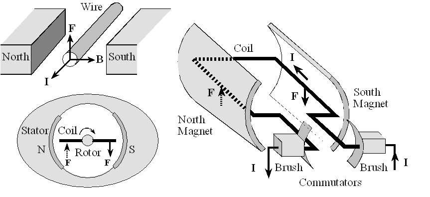
Figure 12.7. A brushed DC motor uses a commutator to flip the coil current.
In the LED interface the microcontroller was able to control electrical power to the LED in a binary fashion: either all on or all off. Sometimes it is desirable for the microcontroller to be able to vary the delivered power in a variable manner. One effective way to do this is to use pulse width modulation (PWM). The basic idea of PWM is to create a digital output wave of fixed frequency, but allow the microcontroller to vary its duty cycle. The system is designed in such a way that High+Low is constant (meaning the frequency is fixed). The duty cycle is defined as the fraction of time the signal is high:
![]()
Hence, duty cycle varies from 0 to 1. We interface this digital output wave to an external actuator (like a DC motor), such that power is applied to the motor when the signal is high, and no power is applied when the signal is low. We purposely select a frequency high enough so the DC motor does not start/stop with each individual pulse, but rather responds to the overall average value of the wave. The average value of a PWM signal is linearly related to its duty cycle and is independent of its frequency. Let P (P=V*I) be the power to the DC motor, shown in Figure 12.8, when the PA5 signal is high. Under conditions of constant speed and constant load, the delivered power to the motor is linearly related to duty cycle.
Delivered Power
= ![]()
Unfortunately, as speed and torque vary, the developed emf will affect delivered power. Nevertheless, PWM is a very effective mechanism, allowing the microcontroller to adjust delivered power.
The resistance in the coil (R) comes from the long wire that goes from the + terminal to the – terminal of the motor, see Figure 12.8. The inductance in the coil (L) arises from the fact that the wire is wound into coils to create the electromagnetics. The coil itself can generate its own voltage (emf) because of the interaction between the electric and magnetic fields. If the coil is a DC motor, then the emf is a function of both the speed of the motor and the developed torque (which in turn is a function of the applied load on the motor.) Because of the internal emf of the coil, the current will depend on the mechanical load. For example, a DC motor running with no load might draw 100 mA, but under load (friction) the current may jump to 1 A.
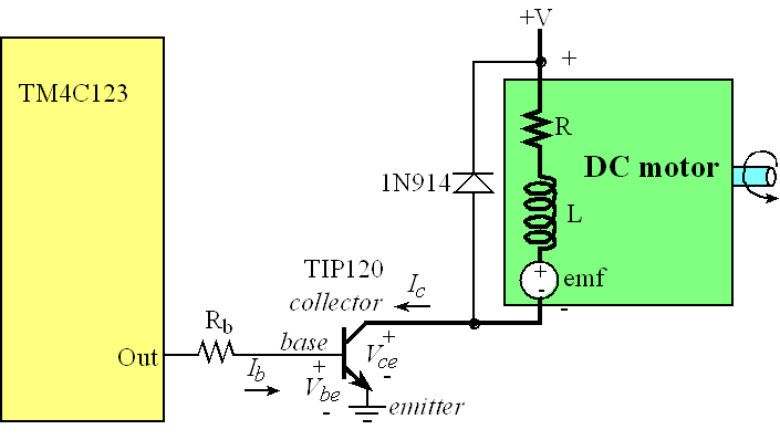
Figure 12.8. The system uses a transistor to turn the motor on and off.
There are lots of motor driver chips, but we will use an NPN Darlington transistor, e.g., TIP120, to allow the software to turn a motor on and off. If the port output is low, no current can flow into the base, so the TIP120 transistor is off, and the collector current, IC, will be zero. If the port output is high, current does flow into the base and VBE goes above VBEsat turning on the TIP120 transistor. The transistor is in the linear range if VBE ≤ VBEsat and Ic = hfe·Ib. The transistor is in the saturated mode if VBE ≥ VBEsat, VCE = 0.7V and Ic < hfe·Ib. We select the value of the Rb resistor to operate the transistor in its saturated mode. We start with the desired motor current, which will be the collector current Ic. The voltage across the coil will be the V - VCE. Next, we calculate the needed base current (Ib) given the current gain of the NPN
Ib = Ic /hfe
knowing the current gain of the NPN (hfe), see Table 12.7. Finally, given the output high voltage of the microcontroller (VOH is about 3.3 V) and base-emitter voltage of the NPN (VBEsat) needed to activate the transistor, we can calculate the desired interface resistor.
Rb ≤ (VOH - VBEsat)/ Ib = hfe *(VOH - VBEsat)/ Ic
The inequality means we can choose a smaller resistor, creating a larger Ib. Because the hfe of the transistors can vary a lot, it is a good design practice to make the Rb resistor 0.1 to 0.5 times the value shown in the above equation. Since the transistor is saturated, the increased base current produces the same VCE and thus the same coil current.
|
Parameter |
TIP120 (at ICE=200mA) |
|
hfe |
900 |
|
VBEsat |
1.3 V |
|
VCE |
0.7 V |
|
ICE |
Up to 5A |
Table 12.7. Design parameters for the TIP120.
Example 12.2. Design an interface for an 8-V 200-mA geared DC motor. SW1 will make the motor spin faster and SW2 will make it spin slower.
Solution: We will use the TIP120 circuit as shown in Figure 12.8 because the TIP120 can sink many times the current needed for this motor. We select a +8.4V battery supply and connect it to the positive side of the motor. Just like the stepper motor, when designing with motors we will not use the 3.3V or +5V from the LaunchPad. Although the current is only 200 mA when spinning unloaded, it will increase to 1 A if the motor experiences mechanical friction. The needed base current is
Ib = Icoil /hfe = 200mA/900 = 0.22mA
The desired interface resistor.
Rb ≤ (VOH - Vbe)/ Ib = (3.3-1.3)/0.22mA = 9 kΩ
To cover the variability in hfe, we will use a 1 kΩ resistor instead of the 9 kΩ. The actual voltage across the motor when active will be +8.4-0.7 = 7.7V. Motors and transistors vary a lot, so it is appropriate to experimentally verify the design by measuring the voltages and currents.
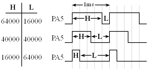
Program 12.7 is used to control the motor. Interrupts are triggered on the falling edges of PF4 and PF0. The period of the PWM output is chosen to be about 10 times shorter than the time constant of the motor. The electronic driver will turn on and off every 1ms, but the motor only responds to the average level. The software sets the duty cycle of the PWM to adjust the delivered power. When active, the interface will drive +7.65 V across the motor. The actual current will be a function of the friction applied to the shaft. The software maintains H+L to be 80,000 (Figure 12.9); this will set the period on PA5 to be a fixed value of 1ms. The duty cycle, L/(H+L), will specify the amount of electrical power delivered to the motor.
|
Figure 12.9. The duty cycle of the PWM output sets the power to the motor. |
Video 12.4b. Duty Cycle Flowchart and Timing |
The interface for one motor is shown in Figure 12.10. If the robot has two motors then a second copy of the TIP120 circuit will be needed. The Port F edge-triggered interrupt will change the duty cycle by ±10% depending on whether the operator touches SW1 or SW2. Since the two ISRs pass data (H,L passed from GPIOPortF_Handler to SysTick_Handler), we will set the interrupt priorities to be equal. With equal priorities neither ISR will interrupt the other. This way, the global variables H,L will always be in a consistent state.
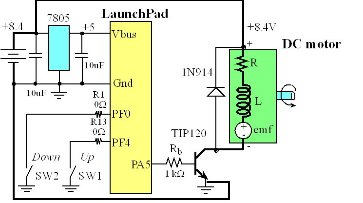
Figure 12.10. DC motor interface (bold lines show path of the large current).
|
uint32_t H,L; void Motor_Init(void){ SYSCTL_RCGCGPIO_R |= 0x00000001; // activate clock for port A H = L = 8000; // 10% GPIO_PORTA_DIR_R |= 0x20; // make PA5 out GPIO_PORTA_DR8R_R |= 0x20; // enable 8 mA drive on PA5 GPIO_PORTA_DEN_R |= 0x20; // enable digital I/O on PA5 GPIO_PORTA_DATA_R &= ~0x20; // make PA5 low NVIC_ST_CTRL_R = 0; // disable SysTick during setup NVIC_ST_RELOAD_R = L-1; // reload value for 500us NVIC_ST_CURRENT_R = 0; // any write to current clears it NVIC_SYS_PRI3_R = (NVIC_SYS_PRI3_R&0x00FFFFFF)|0x40000000; // priority 2 NVIC_ST_CTRL_R = 0x00000007; // enable with core clock and interrupts } void SysTick_Handler(void){ if(GPIO_PORTA_DATA_R&0x20){ // toggle PA5 GPIO_PORTA_DATA_R &= ~0x20; // make PA5 low NVIC_ST_RELOAD_R = L-1; // reload value for low phase } else{ GPIO_PORTA_DATA_R |= 0x20; // make PA5 high NVIC_ST_RELOAD_R = H-1; // reload value for high phase } } void Switch_Init(void){ uint32_t volatile delay; SYSCTL_RCGCGPIO_R |= 0x00000020; // (a) activate clock for port F delay = SYSCTL_RCGCGPIO_R; GPIO_PORTF_LOCK_R = 0x4C4F434B; // unlock GPIO Port F GPIO_PORTF_CR_R = 0x11; // allow changes to PF4,0 GPIO_PORTF_DIR_R &= ~0x11; // (c) make PF4,0 in (built-in button) GPIO_PORTF_DEN_R |= 0x11; // enable digital I/O on PF4,0 GPIO_PORTF_PUR_R |= 0x11; // enable weak pull-up on PF4,0 GPIO_PORTF_IS_R &= ~0x11; // (d) PF4,PF0 is edge-sensitive GPIO_PORTF_IBE_R &= ~0x11; // PF4,PF0 is not both edges GPIO_PORTF_IEV_R &= ~0x11; // PF4,PF0 falling edge event GPIO_PORTF_ICR_R = 0x11; // (e) clear flags 4,0 GPIO_PORTF_IM_R |= 0x11; // (f) arm interrupt on PF4,PF0 NVIC_PRI7_R = (NVIC_PRI7_R&0xFF00FFFF)|0x00400000; // (g) priority 2 NVIC_EN0_R = 0x40000000; // (h) enable interrupt 30 in NVIC } // L range: 8000,16000,24000,32000,40000,48000,56000,64000,72000 // power: 10% 20% 30% 40% 50% 60% 70% 80% 90% void GPIOPortF_Handler(void){ // called on touch of either SW1 or SW2 if(GPIO_PORTF_RIS_R&0x01){ // SW2 touch GPIO_PORTF_ICR_R = 0x01; // acknowledge flag0 if(L>8000) L = L-8000; // slow down } if(GPIO_PORTF_RIS_R&0x10){ // SW1 touch GPIO_PORTF_ICR_R = 0x10; // acknowledge flag4 if(L<72000) L = L+8000; // speed up } H = 80000-L; // constant period of 1ms, variable duty cycle } int main(void){ DisableInterrupts(); // disable interrupts while initializing PLL_Init(); // bus clock at 80 MHz Motor_Init(); // output from PA5, SysTick interrupts Switch_Init(); // arm PF4, PF0 for falling edge interrupts EnableInterrupts(); // enable after all initialization are done while(1){ // main program is free to perform other tasks WaitForInterrupt(); // low power mode } } Program 12.7. Motor output using a periodic interrupt. Switches are used to adjust the power (C12_DCMotor). |
Video 12.4c. PWM Software control of DC Motor |
Reprinted with approval from Embedded Systems: Introduction to ARM Cortex-M Microcontrollers, 2014, ISBN: 978-1477508992, http://users.ece.utexas.edu/~valvano/arm/outline1.htm
and from Embedded Systems: Real-Time Interfacing to Arm® Cortex™-M Microcontrollers, 2014, ISBN: 978-1463590154, http://users.ece.utexas.edu/~valvano/arm/outline.htm
