Digital
Logic
Embedded Systems - Shape
The World
Jonathan Valvano and Ramesh Yerraballi
This appendix presents digital logic. We will first define what it means to be digital, and then introduce logic, voltages, gates, flip flops, registers, adders and memory. This chapter is foundational, laying the ground work for the remainder of the class.
Table of Contents:
- DL.1. Binary Information Implemented with MOS transistors
- DL.2. Digital Logic: AND OR EOR NAND NOR ENOR
- DL.3. Boolean Algebra
- DL.4. Flip-flops
- DL.5. Tristate Logic
- DL.6. Open Collector Logic
- DL.7. Binary Adder
- DL.8. Digital Information stored in Memory
Learning Objectives:
- Understand N-channel and P-channel MOS transistors.
- Learn digital logic as implemented on a computer.
- Know how to build simple logic from transistors.
- Learn how to construct the basic components of a computer from the logic gates.
- Know the terms: flip flop, register, binary adder and memory.
Information is stored on the computer in binary form. A binary bit can exist in one of two possible states. In positive logic, the presence of a voltage is called the ‘1’, true, asserted, or high state. The absence of a voltage is called the ‘0’, false, not asserted, or low state. Figure DL.1.1 shows the output of a typical complementary metal oxide semiconductor (CMOS) circuit. The left side shows the condition with a true bit, and the right side shows a false. The output of each digital circuit consists of a p-type transistor “on top of” an n-type transistor. In digital circuits, each transistor is essentially on or off. If the transistor is on, it is equivalent to a short circuit between its two output pins. Conversely, if the transistor is off, it is equivalent to an open circuit between its outputs pins.
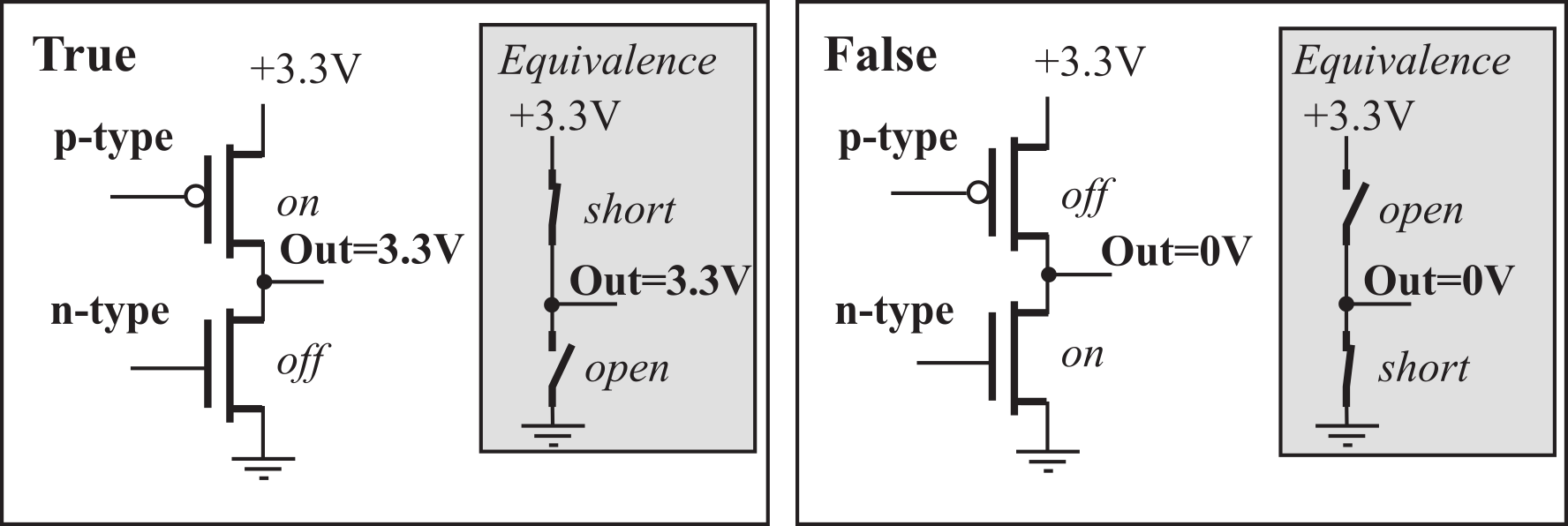
Figure DL.1.1. A binary bit is true if a voltage is present and false if the voltage is 0.
In this section, we will give just a little taste of how the computer digital logic in the computer works. Transistors made with metal oxide semiconductors are called MOS. In the digital world MOS transistors can be thought of as voltage controlled switches. Circuits made with both p-type and n-type MOS transistors are called complementary metal oxide semiconductors or CMOS. The 74HC04 is a high-speed CMOS NOT gate, as shown in Figure DL.2.1.

Figure DL.2.1. CMOS implementation of a NOT gate.
Video 1 Design of a NOT gate with transistors
There are just a few rules one needs to know for understanding how CMOS transistor-level circuits work. Each transistor acts like a switch between its source and drain pins. In general, current can flow from source to drain across an active p-type transistor, and no current will flow if the switch is open. From a first approximation, we can assume no current flows into or out of the gate. For a p-type transistor, the switch will be closed (transistor active) if its gate is low. A p-type transistor will be off (its switch is open) if its gate is high.
The gate on the n-type works in a complementary fashion, hence the name complementary metal oxide semiconductor. For an n-type transistor, the switch will be closed (transistor active) if its gate is high. An n-type transistor will be off (its switch is open) if its gate is low. Therefore, consider the two possibilities for the circuit in Figure 4.4. If the input A is high (+3.3V), then the p-type transistor is off and the n-type transistor is active. The closed switch across the source-drain of the n-type transistor will make the output low (0V). Conversely, if A is low (0V), then p-type transistor is active and the n-type transistor is off. The closed switch across the source-drain of the p-type transistor will make the output high (+3.3V).
The AND, OR, EOR digital logic takes two inputs and produces one output; see Figure DL.2.2 and Table DL.2.1. We can understand the operation of the AND gate by observing the behavior of its six transistors. If both inputs A and B are high, both T3 and T4 will be active. Furthermore, if A and B are both high, T1 and T2 will be off. In this case, the signal labeled ~(A&B) will be low because the T3–T4 switch combination will short this signal to ground. If A is low, T1 will be active and T3 off. Similarly, if B is low, T2 will be active and T4 off. Therefore if either A is low or if B is low, the signal labeled ~(A&B) will be high because one or both of the T1, T2 switches will short this signal to +3.3V. Transistors T5 and T6 create a logical complement, converting the signal ~(A&B) into the desired result of A&B. We can use the and operation to extract, or mask, individual bits from a value.
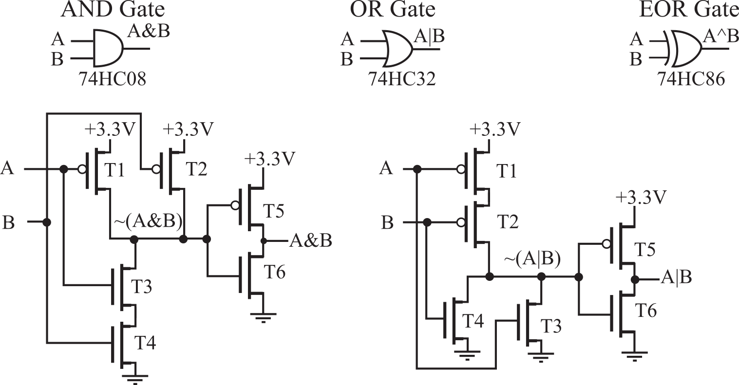
Figure DL.2.2. Logical operations can be implemented with discrete transistors or digital gates.
|
A |
B |
AND |
NAND |
OR |
NOR |
EOR |
Ex NOR |
|
0 |
0 |
0 |
1 |
0 |
1 |
0 |
1 |
|
0 |
1 |
0 |
1 |
1 |
0 |
1 |
0 |
|
1 |
0 |
0 |
1 |
1 |
0 |
1 |
0 |
|
1 |
1 |
1 |
0 |
1 |
0 |
0 |
1 |
|
Symbol |
A&B |
~(A&B) |
A|B |
~(A|B) |
A^B |
~(A^B) |
|
Table DL.2.1. Two-input one-output logical operations.
We can understand the operation of the OR gate by observing the behavior of its six transistors. If both inputs A and B are low, both T1 and T2 will be active. Furthermore, if A and B are both low, T3 and T4 will be off. In this case, the signal labeled ~(A|B) will be high because the T1–T2 switch combination will short this signal to +3.3V. If A is high, T3 will be active and T1 off. Similarly, if B is high, T4 will be active and T2 off. Therefore if either A is high or if B is high, the signal labeled ~(A|B) will be low because one or both of the T3, T4 switches will short this signal to ground. Transistors T5 and T6 create a logical complement, converting the signal ~(A|B) into the desired result of A|B. We use the OR operation to set individual bits.
When writing software we will have two kinds of logic operations. When operating on numbers (collection of bits) we will perform logic operations bit by bit. In other words, the operation is applied independently on each bit. In C, the logic operator for AND is &. For example, if number A is 01100111 and number B is 11110000 then
A = 01100111
B = 11110000
A&B 01100000
The other type of logic operation occurs when operating on Boolean values. In C, the condition false is represented by the value 0, and true is any nonzero value. In this case, if the Boolean A is 01100111 and B is 11110000 then both A and B are true. The standard value for true is the value 1. In C, the Boolean operator for AND is &&. Performing Boolean operation yields
A = 01100111
B = 11110000
A&&B 1
In C, the logic operator for OR is |. The logic operation is applied independently on each bit. E.g.,
A = 01100111
B = 11110000
A|B 11110111
In C, the Boolean operator for OR is ||. Performing Boolean operation of true OR true yields true. Although 1 is the standard value for a true, any nonzero value is considered as true.
A = 01100111
B = 11110000
A||B 1
Other convenient logical operators are shown as digital gates in Figure DL.2.3. The NAND operation is defined by an AND followed by a NOT. If you compare the transistor-level circuits in Figures DL.2.2 and DL.2.3, it would be more precise to say AND is defined as a NAND followed by a NOT. Similarly, the OR operation is a NOR followed by a NOT. The exclusive NOR operation implements the bit-wise equals operation.
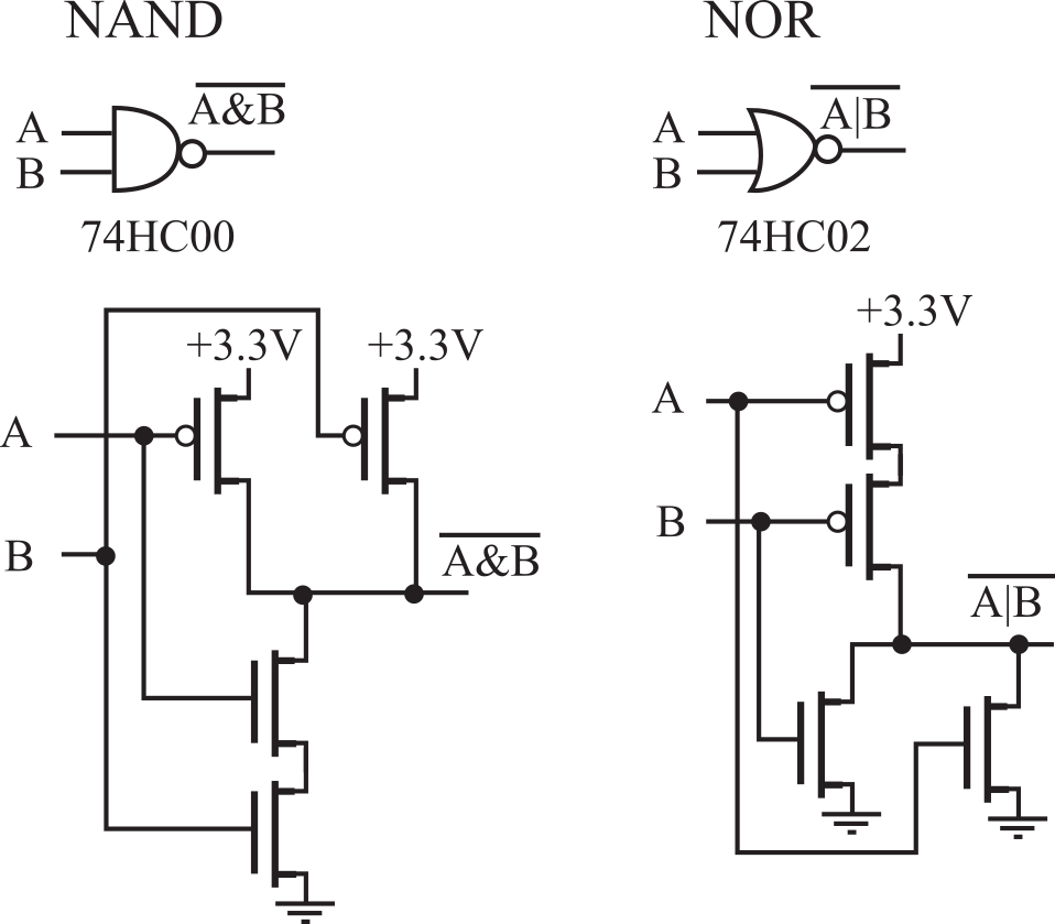
Figure DL2.3. Other logical operations can also be implemented with MOS transistors.
Boolean Algebra is the mathematical framework for digital logic. Some fundamental laws of Boolean Algebra are listed in Table DL.3.1. With these laws, we consider A, B, C either as Booleans or as individual bits of a logic operation.
|
A & B = B & A |
Commutative
Law |
Table DL.3.1. Fundamental laws of Boolean Algebra.
. Let A bit an 8-bit number, and consider the operation B=A&0x20, where A&0x20 is performed bit by bit. Now, if we consider B as a Boolean value, what is the relationship between A and B?
. Let C be an 8-bit number and consider the operation C=C&0xDF. How does this operation affect C?
. Let D bit an 8-bit number, and consider the operation D=D|0x20. How does this operation affect D?
When multiple operations occur in a single expression, precedence is used to determine the order of operation. Usually NOT is evaluated first, then AND, and then OR. This order can be altered using parentheses.
There are multiple
ways to symbolically represent the digital logic functions. For
example, ~A A’ ![]() !A
and ⌐A are five ways to represent NOT(A). One can
use the pipe symbol (|) or the plus sign to represent logical OR: A|B
A+B. In this class we will not use the plus sign to
represent OR to avoid confusion with arithmetic addition. One can use
the ampersand symbol (&) or a multiplication sign (* •
× ) to represent logical AND:
A&B A•B. In this class we
will not use the multiplication sign to represent AND to avoid
confusion with arithmetic multiplication. Another symbolic rule is
adding a special character (* n \) to a name to signify the signal is
negative logic (0 means true and 1 means false). These symbols do not
signify an operation, but rather are part of the name used to clarify
its meaning. E.g., Enable* is a signal than means enable when the
signal is zero.
!A
and ⌐A are five ways to represent NOT(A). One can
use the pipe symbol (|) or the plus sign to represent logical OR: A|B
A+B. In this class we will not use the plus sign to
represent OR to avoid confusion with arithmetic addition. One can use
the ampersand symbol (&) or a multiplication sign (* •
× ) to represent logical AND:
A&B A•B. In this class we
will not use the multiplication sign to represent AND to avoid
confusion with arithmetic multiplication. Another symbolic rule is
adding a special character (* n \) to a name to signify the signal is
negative logic (0 means true and 1 means false). These symbols do not
signify an operation, but rather are part of the name used to clarify
its meaning. E.g., Enable* is a signal than means enable when the
signal is zero.
. Let C bit an 8-bit number. Are these two operations the same or different? C=C&0xDF C=C&(~0x20)
While we’re introducing digital circuits, we need digital storage devices, which are essential components used to make registers and memory. The simplest storage device is the set-reset latch. One way to build a set-reset latch is shown on the left side of Figure DL.4.1. If the inputs are S*=0 and R*=1, then the Q output will be 1. Conversely, if the inputs are S*=1 and R*=0, then the Q output will be 0. Normally, we leave both the S* and R* inputs high. We make the signal S* go low, then back high to set the latch, making Q=1. Conversely, we make the signal R* go low, then back high to reset the latch, making Q=0. If both S* and R* are 1, the value on Q will be remembered or stored. This latch enters an unpredictable mode when S* and R* are simultaneously low.
The gated D latch is also shown in Figure DL.4.1. The front-end circuits take a data input, D, and a control signal, W, and produce the S* and R* commands for the set-reset latch. For example, if W=0, then the latch is in its quiescent state, remembering the value on Q that was previously written. However, if W=1, then the data input is stored into the latch. In particular, if D=1 and W=1, then S*=0 and R*=1, making Q=1. Furthermore, if D=0 and W=1, then S*=1 and R*=0, making Q=0. So, to use the gated latch, we first put the data on the D input, next we make W go high, and then we make W go low. This causes the data value to be stored at Q. After W goes low, the data does not need to exist at the D input anymore. If the D input changes while W is high, then the Q output will change correspondingly. However, the last value on the D input is remembered or latched when the W falls, as shown in Table DL.4.1.
The D flip-flop, shown on the right of Figure DL.4.1, can also be used to store information. D flip-flops are the basic building block of RAM and registers on the computer. To save information, we first place the digital value we wish to remember on the D input, and then give a rising edge to the clock input. After the rising edge of the clock, the value is available at the Q output, and the D input is free to change. The operation of the clocked D flip-flop is defined on the right side of Table 3. The 74HC374 is an 8-bit D flip-flop, such that all 8 bits are stored on the rising edge of a single clock. The 74HC374 is similar in structure and operation to a register, which is high-speed memory inside the processor. If the gate (G) input on the 74HC374 is high, its outputs will be HiZ (floating), and if the gate is low, the outputs will be high or low depending on the stored values on the flip-flop. The D flip-flops are edge-triggered, meaning that changes in the output occur at the rising edge of the input clock.

Figure DL.4.1. Digital storage elements.
|
D |
W |
Q |
|
D |
clock |
Q |
|
0 |
0 |
Qold |
|
0 |
0 |
Qold |
|
1 |
0 |
Qold |
|
0 |
1 |
Qold |
|
0 |
1 |
0 |
|
1 |
0 |
Qold |
|
1 |
1 |
1 |
|
1 |
1 |
Qold |
|
0 |
↓ |
0 |
|
0 |
↑ |
0 |
|
1 |
↓ |
1 |
|
1 |
↑ |
1 |
Table DL.4.1. D flip-flop operation. Qold is the value of the D input at the time of fall of W or rise of clock.
DL.5. Tristate Logic
The tristate driver, shown in Figures DL.5.1 and DL.5.2, can be used dynamically control signals within the computer. It is called tristate because there are three possible outputs: high, low, and HiZ.
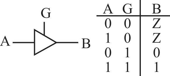
Figure DL.5.1. A tristate driver. If G is low, then Y is HiZ.
The tristate driver is an essential component from which computers are built. To activate the driver, we make its gate (G) high. When the driver is active, its output (Y) equals its input (A). To deactivate the driver, we make its G low. When the driver is not active, its output Y floats independent of A. We will also see this floating state with the open collector logic, and it is also called HiZ or high impedance. The HiZ output means the output is neither driven high nor low. The operation of a tristate driver is defined in Table DL.5.1. Normally, we can't connect two digital outputs together. The tristate driver provides a way to connect multiple outputs to the same signal, as long as at most one of the gates is active at a time.
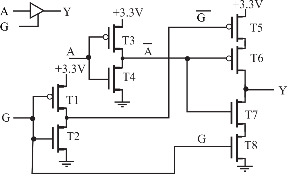
Figure DL.5.2. A tristate driver.
Table DL.5.1 describes how the tristate driver in Figure DL.5.2 works. Transistors T1 and T2 create the logical complement of G. Similarly, transistors T3 and T4 create the complement of A. An input of G=1 causes the driver to be active. In this case, both T5 and T8 will be on. With T5 and T8 on, the circuit behaves like a cascade of two NOT gates, so the output Y equals the input A. However, if the input G=0, both T5 and T8 will be off. Since T5 is in series with the +3.3V, and T8 in series with the ground, the output Y will be neither high nor low. I.e., it will float.
|
A |
G |
T1 |
T2 |
T3 |
T4 |
T5 |
T6 |
T7 |
T8 |
Y |
|
0 |
1 |
on |
off |
on |
off |
on |
off |
on |
on |
0 |
|
1 |
1 |
on |
off |
off |
on |
on |
on |
off |
on |
1 |
|
0 |
0 |
off |
on |
on |
off |
off |
off |
on |
off |
HiZ |
|
1 |
0 |
off |
on |
off |
on |
off |
on |
off |
off |
HiZ |
Table DL.5.1. Tristate driver operation. HiZ is the floating state, such that the output is not high or low.
DL.6. Open Collector Logic or Open Drain Logic
The output of an open collector gate, drawn with the ‘×’, has two states low (0V) and HiZ (floating) as shown in Figure DL.6.1. Consider the operation of the transistor-level circuit for the 74HC05. If A is high (+3.3V), the transistor is active, and the output is low (0V). If A is low (0V), the transistor is off, and the output is neither high nor low. In general, we can use an open collector NOT gate to switch current on and off to a device, such as a relay, an LED, a solenoid, or a small motor. The 74HC05, the 74LS05, the 7405, and the 7406 are all open collector NOT gates. 74HC04 is high-speed CMOS and can only sink up to 4 mA when its output is low. Since the 7405 and 7406 are transistor-transistor-logic (TTL) they can sink more current. In particular, the 7405 has a maximum output low current (IOL) of 16 mA, whereas the 7406 has a maximum IOL of 40 mA.
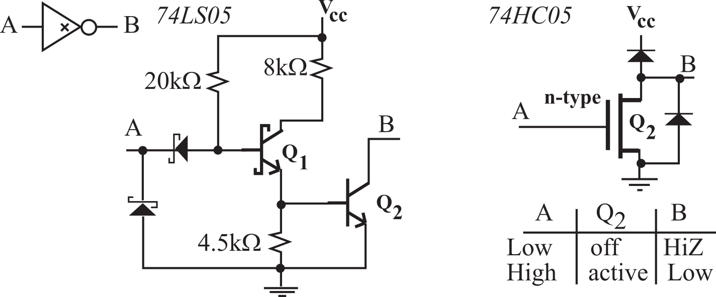
Figure DL.6.1. Two transistor implementations of an open collector NOT gate.
The computer performs many arithmetic and logic operations. We will show one of them to illustrate some of the computation possible in the computer. We begin the design of an adder circuit with a simple subcircuit called a binary full adder, as shown in Figure DL.7.1. There are two binary data inputs A, B, and a carry input, Cin. There is one data output, Sout, and one carry output, Cout. As shown in Table DL.7.1, Cin, A, and B are three independent binary inputs each of which could be 0 or 1. These three inputs are added together (the sum could be 0, 1, 2, or 3), and the result is encoded in the two-bit binary result with Cout as the most significant bit and Sout as the least significant bit. Cout is true if the sum is 2 or 3, and Sout is true if the sum is 1 or 3.
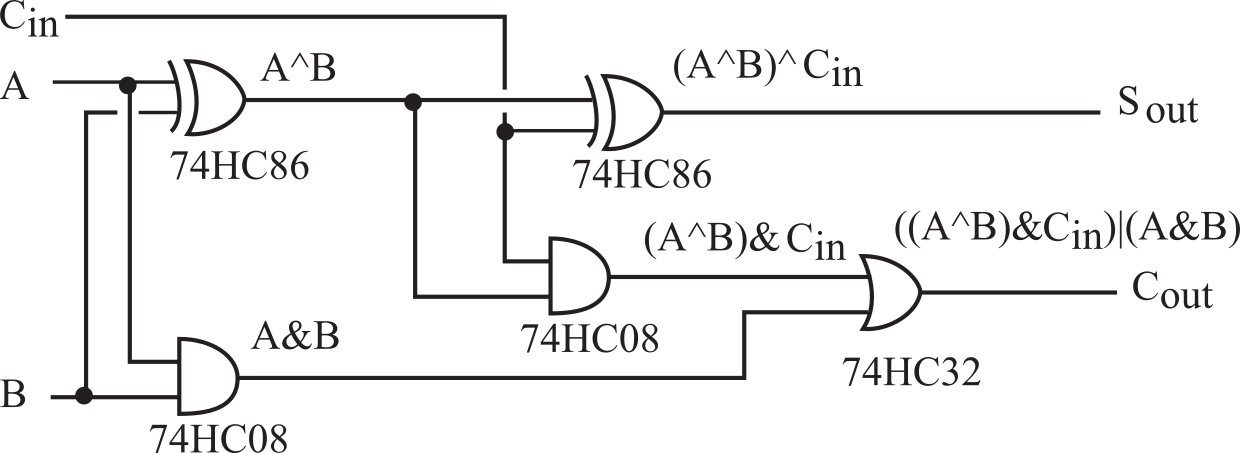
Figure DL.7.1. A binary full adder.
|
A |
B |
Cin |
A+B+Cin |
Cout |
Sout |
|
0 |
0 |
0 |
0 |
0 |
0 |
|
0 |
0 |
1 |
1 |
0 |
1 |
|
0 |
1 |
0 |
1 |
0 |
1 |
|
0 |
1 |
1 |
2 |
1 |
0 |
|
1 |
0 |
0 |
1 |
0 |
1 |
|
1 |
0 |
1 |
2 |
1 |
0 |
|
1 |
1 |
0 |
2 |
1 |
0 |
|
1 |
1 |
1 |
3 |
1 |
1 |
Table DL.7.1. Input/output response of a binary full adder.
Figure DL.7.2 shows an 8-bit adder formed by cascading eight binary full adders. Similarly, we build a 32-bit adder by cascading 32 binary full adders together. The carry into the 32-bit adder is zero, and the carry out will be saved in the carry bit.
Figure DL.7.2. We make an 8-bit adder cascading eight binary full adders.
For an 8-bit unsigned number, there are only 256 possible values, which are 0 to 255. When we add two 8-bit numbers the sum can be any number from 0 to 510, which is a 9-bit number. The 9-bit result in Figure DL.7.2 exists as the 8 bits R7–R0 plus carry.
We can think of 8-bit unsigned numbers as positions along a circle, like a clock. There is a discontinuity in the clock at the 0|255 interface; everywhere else adjacent numbers differ by ±1. If we add two unsigned numbers, we start at the position of the first number a move in a clockwise direction the number of steps equal to the second number. If 96+64 is performed in 8-bit unsigned precision, the correct result of 160 is obtained. In this case, the carry bit will be 0 signifying the answer is correct. On the other hand, if 224+64 is performed in 8-bit unsigned precision, the incorrect result of 32 is obtained. In this case, the carry bit will be 1, signifying the answer is wrong.
. If A has the value 100 (0x64) and B has the value 50 (0x32), what will be the value of the output (R7-R0) of the circuit in Figure DL.7.2? Also what will the carry signal be?
. If A has the value 255 (0xFF) and B has the value 2 (0x02), what will be the value of the output (R7-R0) of the circuit in Figure DL.7.2? Also what will the carry signal be?
Memory is a collection of hardware elements in a computer into which we store information, as shown in Figure DL.8.1. For most computers in today’s market, each memory cell contains one byte of information, and each byte has a unique and sequential address. The memory is called byte-addressable because each byte has a separate address. The address of a memory cell specifies its physical location, and its content is the data. When we write to memory, we specify an address and 8, 16, or 32 bits of data, causing that information to be stored into the memory. Typically data flows from processor into memory during a write cycle. When we read from memory we specify an address, causing 8, 16, or 32 bits of data to be retrieved from the memory. Typically data flows from memory into the processor during a read cycle. Read Only Memory, or ROM, is a type of memory where the information is programmed or burned into the device, and during normal operation it only allows read accesses. Random Access Memory (RAM) is used to store temporary information, and during normal operation we can read from or write data into RAM. The information in the ROM is nonvolatile, meaning the contents are not lost when power is removed. In contrast, the information in the RAM is volatile, meaning the contents are lost when power is removed. The system can quickly and conveniently read data from a ROM. It takes a comparatively long time to program or burn data into a ROM. Writing to Flash ROM is a two-step process. First, the ROM is erased, causing all the bits to become 1. Second, the system writes zeroes into the ROM as needed. Each of these two steps requires around 1 ms to complete. In contrast, it is fast and easy to both read data from and write data into a RAM. Writing to RAM is about 100,000 times faster (on the order of 10 ns). ROM on the other hand is much denser than RAM. This means we can pack more ROM bits into a chip than we can pack RAM bits. Most microcontrollers have much more ROM than RAM.
Figure DL.8.1. Memory is a sequential collection of data storage elements.
In the computer, we can build an 8-bit storage element, shown logically as Figure DL.8.1, by combining 8 flip-flops. This basic storage element is called a register, as shown in Figure DL.8.2. A bus is a collection of wires used to pass data from one place to another. In this circuit, the signals D7–D0 represent the data bus. Registers on the CortexM microcontrollers are 32-bits wide, but in this example we show an 8-bit register. We call it storage because as long the circuit remains powered, the digital information represented by the eight voltages Q7–Q0 will be remembered. There are two operations one performs on a register: write and read. To perform a write, one first puts the desired information on the 8 data bus wires (D7–D0). As you can see from Figure DL.8.2, these data bus signals are present on the D inputs of the 8 flip-flops. Next, the system pulses the Write signal high then low. This Write pulse will latch or store the desired data into the 8 flip-flops. The read operation will place a copy of the register information onto the data bus. Notice the gate signals of the tristate drivers are negative logic. This means if the Read* signal is high, the tristate drivers are off, and this register does not affect signals on the bus. However, the read operation occurs by setting the Read* signal low, which will place the register data onto the bus.
. What does negative logic mean?
Figure DL.8.2. Digital logic implementation of a register.
This material was created to teach ECE319K at the University of Texas at Austin
Reprinted with approval from Introduction to Embedded Systems Using the MSPM0+, ISBN: 979-8852536594

Embedded
Systems - Shape the World by Jonathan Valvano and Ramesh Yerraballi is
licensed under a Creative
Commons
Attribution-NonCommercial-NoDerivatives 4.0 International License.
Based on a work at http://users.ece.utexas.edu/~valvano/mspm0/