System-on-Chip
(SoC) Design
ECE382M.20,
Fall 2021
Board
Tutorial
Notes:
•
This
is a tutorial related to the class project.
•
Please
use the discussion board on Piazza for Q&A.
•
Please
check relevant web pages.
1
Overview
The goal of this
tutorial is to:
•
Give an introduction to the Xilinx tools and
the Ultra96 board.
This tutorial includes
the following:
•
Use
of the Ultra96 board to run and co-verify a multiply-and-accumulate (MAC)
example.
•
An
application that reads inputs, calls the hardware function with these inputs
(modifying a HAL implementation adapted from Lab 2), gets the output, and
prints it.
We will use three
Xilinx tools to prototype the application on the board:
•
Vivado HLS is Xilinx’s high-level
synthesis (HLS) tool that is used for C-to-RTL synthesis (you already used Vivado HLS in Lab 3).
•
Vivado Design Suite will be used for
RTL-to-gate synthesis and FPGA bitstream generation.
•
Vivado’s IP Integrator lets you
create complex system designs by instantiating and interconnecting IP cores.
2 Resources and Documentation
Please refer to the
following materials for additional information:
•
The
Xilinx
Vivado HLS Tutorial (UG871) already provided in
Lab 3
•
Vivado Design Suite User Guide, Embedded Design (UG898)
•
Vivado Design Suite Tutorial, Embedded Design (UG940)
3 Example
This example takes two
integers as inputs, calculates their product, and gives the accumulated sum as
the output. The multiplication and accumulation take place in the FPGA, which
is called from the software.
(a)
Hardware
part
1. Download the hardware source code (hls_macc.tar.gz) into your directory and unzip the file:
• The example code, hls_macc.c/.h, is the C source code annotated with Xilinx-specific synthesis directives (pragmas), which are used to automatically infer a bus and register interface.
• The application code
comes with a testbench (hls_macc_test.c).
2.
Launch
Vivado HLS and synthesize the example code. The steps
are equivalent to what you did in Lab 3, following the Vivado HLS Tutorial
(UG871) and/or training materials:
a.
Create
a new project by using the following information:
Project name: hls_macc (or
whatever you want.)
Location: On the LRC machines under/misc/scratch
Top Function: hls_macc
Design Files: hls_macc.c
TestBench Files: hls_macc_test.c
Solution Name: solution1 (or whatever you want)
Clock Period: 4
Part Selection: RTL tool: Auto, Specify:
Parts->Select ‘xczu3eg-sbva484-1-e’
b.
Run
C Simulation
c.
Run
C Synthesis
d.
Run
C/RTL Cosimulation
3.
Click
‘Solution’ -> ‘Export RTL’ -> ‘OK’.
This will make the generated RTL code usable in Vivado Design Suite as a custom
hardware IP. If this step is successful, you will see a zip file appear under
‘solution1’ -> ‘impl’ -> ‘ip’ in the
explorer pane.
4.
Exit
Vivado HLS.
5.
Launch
Vivado Design Suite on an LRC machine:
%
module load xilinx/2018
% vivado
6.
Follow
Steps 2 through 5 of Lab 1 (“Implement Vivado HLS IP on a Zynq
Device”) in Chapter 10 (“Using HLS IP in a Zynq AP SoC Design”)
of the Vivado HLS Tutorial (UG871) to integrate the HLS IP into an overall
system design and generate the FPGA bitstream. Make sure to select a Ultra96v2
setup wherever necessary:
•
‘Boards’
-> ‘Ultra96v2 Evaluation Platform’ when you create a new project
(Step 2.4).
•
Ignore
Steps 4.3-4.5.
•
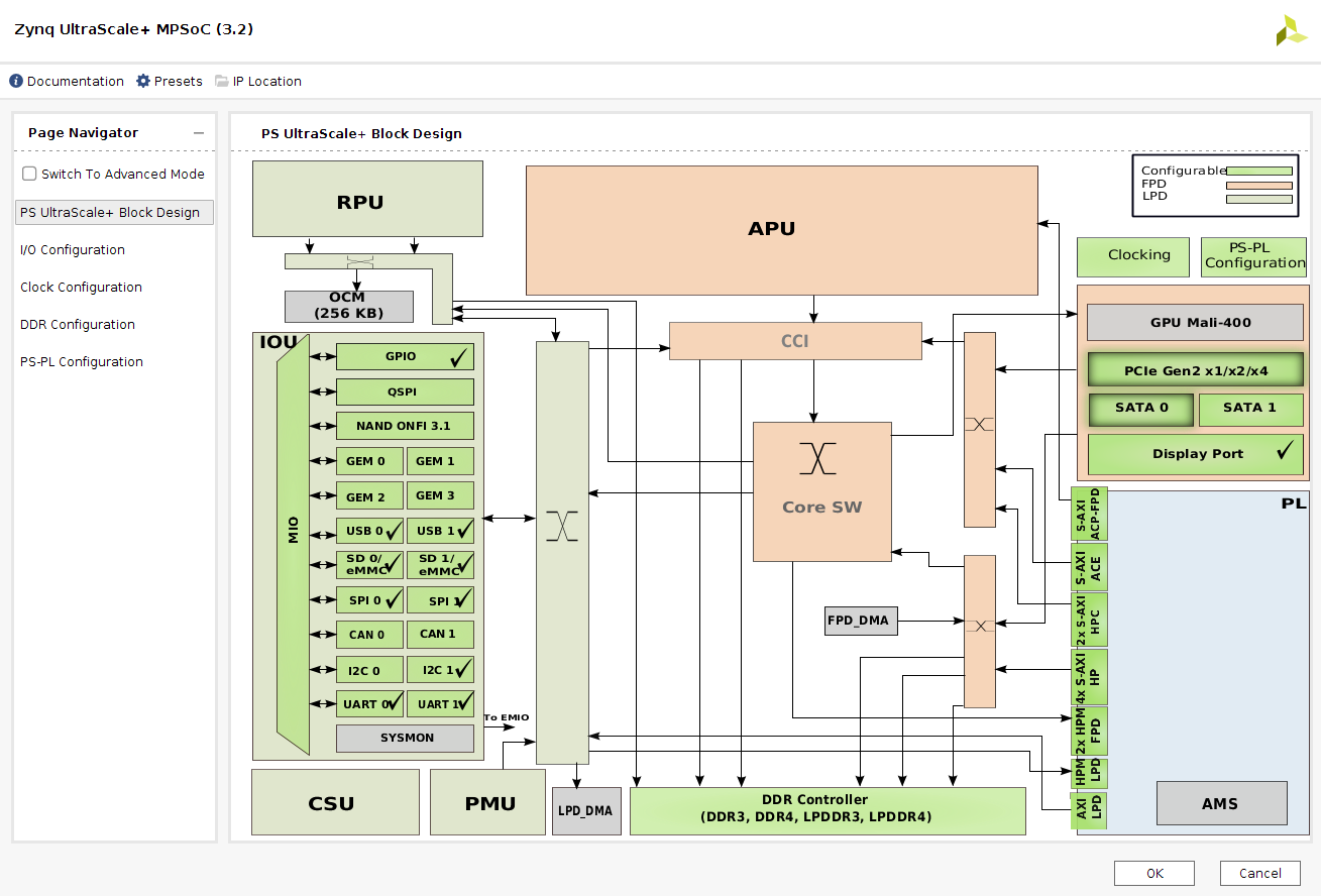
For
Step 4.6, run Block Automation with “zynq_ultra_ps_e_0” and
“Apply Board Preset” both selected. Note: the original instructions
say to deselect the board preset, but we want to select it here. I.e. all
configuration settings are managed by the “Apply Board Preset”
option, there is no manual configuration performed. After this step, the Zynq UltraScale+ IP configuration block should like this:
•
After
Step 4.9, run “Run Connection Automation” a second time.
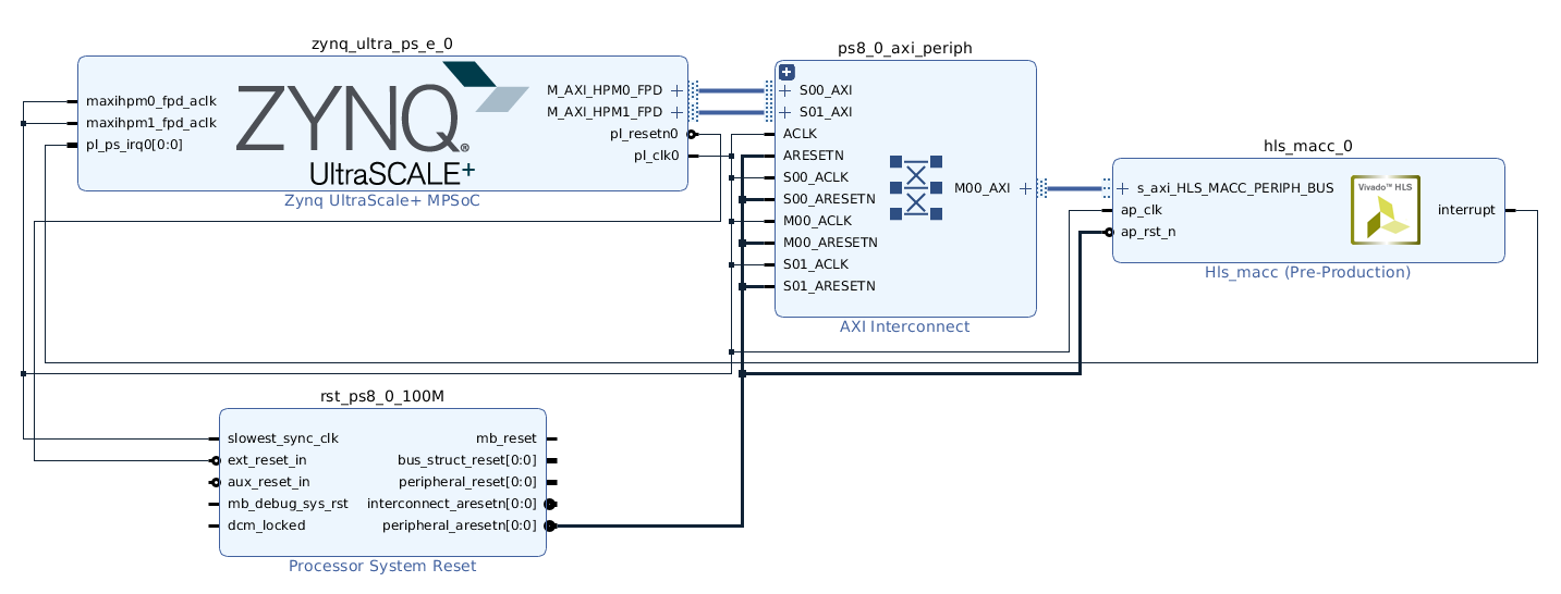
•
Two
icons right of “Validate Design”, you can select “Regenerate
Layout” to prettify your block design and wiring. The Vivado
Block Design should look like the following image:
7.
From
the Vivado menu, select ‘Export’->‘Export Hardware’, make sure the
‘Include Bitstream’ option is enabled, and click OK
8. Then from the Vivado menu, select ‘Launch SDK’ and click OK. Click the ‘system.hdf’ to see your system memory map and relevant information.
(b)
Integrate
hardware on the board
1.
We
first need to integrate the synthesized hardware design into the device tree
blob (DTB) for the Linux kernel using PetaLinux. As
already mentioned in Lab 2, by default, PetaLinux
will create a temporary directory under /tmp that will fill up
fast. You must to log into and use the yoshi machine, which has
local disk space mounted under /homework
that must be used for temporary PetaLinux files,
while PetaLinux projects must be created in the
scratch space (/misc/scratch) on yoshi. Alternatively, you
can work on your own machine using the PetaLinux
Docker image from Lab 2 available here: https://hub.docker.com/r/gerstla/petalinux-systemc.
Important: make sure to pull and work with the 2018.3 version/tag of the Docker
image.
2.
Log
into yoshi, setup the
environment, and create a new PetaLinux project under
/misc/scratch using the board support package (BSP) for our
Ultra96v2 board:
yoshi% module load xilinx/2018
yoshi% source /usr/local/packages/xilinx_2018/petalinux/2018.3/settings.sh
yoshi% umask 022
yoshi% mkdir -p
/misc/scratch/$USER/Project
yoshi% cd /misc/scratch/$USER/Project
yoshi% petalinux-create -t project –n PetaLinux
-s /home/projects/gerstl/ece382m/ultra96v2_oob_2018_3.bsp
yoshi% cd PetaLinux
3.
Configure
the new project by pointing to the hardware description produced by the Xilinx
SDK, and then configure PetaLinux to use a temporary directory under /homework and
to boot from an SD card image:
yoshi% petalinux-config --get-hw-description=<vivado_dir>/<project_name>/<project_name>.sdk/design_1_wrapper_hw_platform_0/ -p ./
Select Yocto
Settings->TMPDIR Location->/homework/<unique directory name>
Select Image Packaging Configuration->Root filesystem
type->SD Card
Save the config and exit
4.
Now
build the DTB:
yoshi% petalinux-build -c device-tree
5.
The
new DTB file is located under ./images/linux. You should see system.dtb and system.bit there.
6.
If
you want to modify the device tree, you can use the dtc tool to decompile the system.dtb file into a system.dts source, edit it, and
then compile it back into a binary DTB blob as described in Lab 2.
7.
Next,
we need to copy the new DTB into the \boot partition of the board. The boot partition on
the SD card of the board is different from the \boot directory that is part of the root filesystem that
you see when logged into the board. As such, you either need to use an SD card
reader to access the SD card from your laptop/PC, or, alternatively, you can simply
mount the \boot partition directly
from the board as the root user:
$ sudo mount /dev/mmcblk0p1 /boot
8.
Now
copy the updated DTB file and the FPGA bitstream into the \boot partition. First back
up the current configuration on your SD card by making dated copies of the original
DTB and bitstream files:
$ cd /boot
$ mv system.dtb system.dtb.`date +%m.%d.%y`
$ mv system.bit system.bit.`date +%m.%d.%y`
Then
copy the new system.dtb and system.bit on the LRC machines to
the /boot partition of the SD
card:
$ sudo scp
<user>@<server>.ece.utexas.edu:<petalinux_dir>
/images/linux/system.bit /boot/system.bit
$ sudo scp
<user>@<server>.ece.utexas.edu:<petalinux_dir>
/images/linux/system.dtb /boot/system.dtb
9. Reboot the board. This will
program the FPGA with the bitstream on the SD card and load the new device tree
into the Linux kernel.
(c)
Software
part
1. Download the source code for a software application example (board_app.tar.gz) that initializes the hardware IP, feeds two operands into the hardware, waits for the result, and reads/prints the output. Note that Vivado HLS will automatically synthesize a set of registers into the hardware that allow the software to configure and control its operation. This includes interrupt enable registers that the above application code needs to first initialize in order for the hardware to generate interrupts. To find the register map automatically defined by Vivado HLS, open the xhls_macc_hw.h file found under ‘<your HLS project> -> <your solution> -> impl -> drivers -> hls_macc_top_v1_0 -> src’ in the Vivado HLS explorer window.
2. The application example includes an updated kernel module and device driver (fpga_drv.c) for the board. This driver was modified from Lab 2 to match the compatible name, properly acknowledge and clear interrupts, and access the correct memory-mapped addresses and interrupt status register in the synthesized hardware. Note that it is always a good idea to double-check the system memory and interrupt mapping and compatible naming, as the kernel and driver rely on this information to interface software and hardware. Once you rebooted your board, check the information of your hardware module in the kernel’s device tree:
$ dtc -I fs /sys/firmware/devicetree/base
You
should see an amba_pl {
… }; section listing your hls_macc device information. An example output should
be as follows:
hls_macc@43c00000 {
xlnx,s-axi-hls-macc-periph-bus-addr-width = <0x6>;
compatible = "xlnx,hls-macc-1.0";
xlnx,s-axi-hls-macc-periph-bus-data-width
= <0x20>;
interrupt-parent = <0x4>;
interrupts = <0x0 0x1d 0x4>;
reg = <0x43c00000 0x10000>;
};
};
In
the above example, the accelerator base address is located at 0x43c00000, the
interrupt ID is 0x1D (29), and the compatible name is "xlnx,hls-macc-1.0". Make sure this
information is aligned to what you have in your driver code. Make necessary
changes in the driver code if necessary.
3.
Compile
the application example and driver code either on the LRC machines as you have
done for Lab 2 or directly on the board. If you cross-compiled the application
on the LRC machines, copy the
compiled example binary and kernel module to the board:
$ scp <user>@<server>.ece.utexas.edu:<path>/example .
$ scp <user>@<server>.ece.utexas.edu:<path>/fpga_drv.ko
.
4. Run the commands to insert the device driver on the board:
$ sudo insmod
fpga_drv.ko
You can look at the kernel logs including any
messages generated by the driver using:
$ dmesg
5. Finally, run the application example:
$ ./example <number1> <number2>
If everything works fine, you should see the
following message in your terminal:
A is <number1>
B is <number2>
C += A*B is <number3>