Fall 2009: EE 382N-4 Unique: 17190
Advanced Embedded Systems Architecture
Lab Assignment #2: Due Nov 1, 2009
AIM: Develop an
Interrupt handler to measure the latency of Linux running on the TLL2020
platform using the I/O ports on the FPGA.
Note: It is an group lab exercise and every group should demonstrate the
working of the code on the board. A group can have a maximum of 4 members.
Tutorial: device_driver + FPGA. Go through this link
first.
In this tutorial, an adder is implemented
on the FPGA. The user application code interacts with the adder through the
device driver.
Specification:
The functional diagram of the required
setup is shown in the block diagram below.
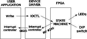
1)
The
user application is the software running on linux
which in turn is running on the ARM processor.
a.
The
application should send a couple of numbers to the device driver and receive
the sum, similar to the demo.
1.
However,
this should be implemented in a while loop (free running – without user
intervention).
2.
For
every two numbers sent to the device driver, the loop will wait for the
interrupt from the FPGA and then issue the command to read the sum.
b.
It
will also host the interrupt signal (SIGIO) handler to measure the latency from
the time the two input data are sent to the FPGA to the time when the interrupt
is received. You can use any C function like gettimeofday() to note the
time.
c.
List
the average, minimum and maximum latency over 10 interrupts as part of your
report.
d.
Discuss
your user application code, as part of your report.
2)
The
device driver will be designed as a loadable module, thus saving kernel memory.
a.
The
device driver file adder.c (from the demo) should be
modified to host the interrupt functions.
b.
The
interrupt functions will initialize the required handlers, request for the
specific interrupt to be serviced etc.
c.
An
example of the same setup for GPIO (as against FPGA) is given below. Relate the
following programs to lecture 9 for a better understanding of the code.
1.
main.c is the user application
2.
mx21_gpio.c is the corresponding device driver
3.
The
interrupt number for the GPIO pin used here is #107. The corresponding
interrupt number for the FPGA is #240.
4.
The MX21 board documentation at
/scratch/Documentation/MC9328MX21RM.pdf. Chapter 15 contains a note about the GPIOs. The configuration details of the GPIO registers are
given in that chapter. This example configures the port PB10 as output and loopbacked to PB11 as input. You do not require these for
the corresponding FPGA implementation.
d.
The above example can be used as a reference to modify the adder.c
e.
Configure the interrupt as rising edge sensitive.
f.
Notify
the application code about the occurrence of the
interrupt using the kill_fasync routine, similar to
the one in mx21_gpio.c
g.
Discuss
the changes that you made to the example device driver (adder.c),
as part of your report.
3)
The
adder is implemented in the FPGA (top.v)
a.
Receives
data from the user application through the device driver.
b.
FPGA
is memory mapped starting from 0xD3000000 and 0xCC000000 of the ARM processor
as stated in the docs.
c.
The
top.v (from the demo) is the verilog file that gets
burned into the FPGA. Modify it
1.
to
raise the interrupt signal when the addition is complete,
1.
MZ_CPLD_MISC14
is the signal corresponding to interrupt #240, in top.v
2.
to
make the interrupt signal a pulse which will go back to zero state
automatically after a certain delay,
3.
to
have one of the DIP switches (or address 0xCC000000 has the value ‘1’ in it) on the board to act as the enable for the
interrupt,
1.
Interrupts
should not be generated when the DIP switch is off (or when 0xCC000000 has say ‘2’ written
into it)
2.
DIP_SW
in top.v is the signal corresponding to the switches.
3.
In
top.v, 0xCC000000 – 0xCFFFFFFF is the bigger of
the memory mapped regions corresponding to the FPGA, the other one is
0xD3000000 – 0xD3FFFFFF
4.
to
toggle an LED whenever address 0xD3000004 is accessed indicating the data
arrival from the ARM processor, and
5.
to
map the interrupt pulse to another LED on the board for observation
d.
Discuss
the changes to top.v, as part of your report.
Deliverables: The
code (user application, device driver, Makefile, top.v) and your report must be zipped and submitted through
the assignment section of Blackboard. Please refrain from sending them as
attachments through email.