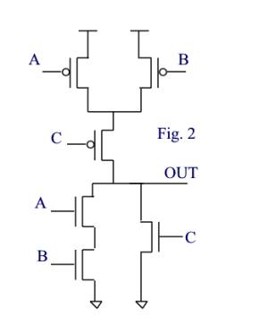
- Fill in the truth table for the transistor-level circuit in Figure 2.
Instructions: You are encouraged to do homework in groups. Remember
to put all group members? names on the solution sheet. Also, remember to
put the unique number of the discussion session you want the homework returned
back to you. Good
luck!!!
1. Same as problem 3.5 in text (pg. 69).
- Fill in the truth table for the transistor-level circuit in Figure
2.
A B C | OUT
------|-----
0 0 0 |
0 0 1 |
0 1 0 |
0 1 1 |
1 0 0 |
1 0 1 |
1 1 0 |
1 1 1 |
2. Same as problem 3.20 in text (pg. 72)
- Referring to Figure 3.30 on page 73 in the text, complete the truth
table for this gate level schematic.
3. Same as problem 3.6 in text (pg. 69)
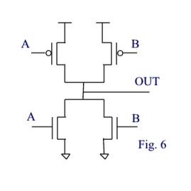
- The circuit in Figure 6 has a flaw.
4. Fill in the truth table for the basic S-R Latch, shown in Figure
7. The left side of the truth table is the current state of the circuit,
and the right side of the truth table is the next state of the circuit
(in other words, the values of a and b a some time after S and R have
been applied). Three lines have been done for you as an example.
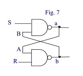
S R a b | a+ b+The last two cases have been filled out for you. You do not have to work them out.
--------|-------
1 1 0 1 |
1 1 1 0 |
1 0 0 1 | 0 1
1 0 1 0 |
0 1 0 1 |
0 1 1 0 |
0 0 0 1 | ? ?
0 0 1 0 | ? ?
5. Implement a 4-to-1 MUX using only 2-to-1 MUXes making sure to properly
connect all of the terminals. Remember that you will have 4 inputs, 2 control
signals, and one output. Write out the truth table for this circuit.
Previous problems 6 and 7 have been taken out, here is the new problem 6:
6. Same as problem 3.19 in text, refer to figure 3.29 in text (pg. 72)