The following program computes the square (k*k) of a positive integer k, stored
in location 0x4000 and stores the result in location 0x4002.
The result is to be treated as a 16-bit unsigned number.
Assumptions:
- A memory access takes 5 cycles
- The system call initiated by the
HALTinstruction takes 20 cycles to execute. This does not include the number of cycles it takes to execute theHALTinstruction itself.
        .ORIG X3000
        AND R0, R0, #0
        LEA R3, NUM
        LDW R3, R3, #0
        LDW R1, R3, #0
        ADD R2, R1, #0
LOOP    ADD R0, R0, R1
        ADD R2, R2, #-1
        BRP LOOP
        STW R0, R3, #1
        HALT
NUM     .FILL x4000
.END- How many cycles does each instruction take to execute on the LC-3b microarchitecture described in Appendix C?
- How many cycles does the entire program take to execute? (answer in terms of k)
- What is the maximum value of k for which this program still works correctly?
- How will you modify this program to support negative values of k? Explain in less than 30 words.
- What is the new range of k?
- In which state(s) in the LC-3b state diagram should the
LD.BENsignal be asserted? Is there a way for the LC-3b to work correctly without theLD.BENsignal? Explain. - Suppose we want to get rid of the
BENregister altogether. Can this be done? If so, explain how. If not, why not? Is it a good idea? Explain. - Suppose we took this further and wanted to get rid of state 0. We can do this by
modifying the microsequencer, as shown in the figure below. What is the 4-bit signal
denoted as
Ain the figure? What is the 1-bit signal denoted asB?

We wish to use the unused opcode “1010” to implement a new instruction ADDM, which (similar
to an IA-32 instruction) adds the contents of a memory location to either the contents of a
register or an immediate value and stores the result into a register. The specification of this instruction is as follows:
Assembler Formats
ADDM DR, SR1, SR2ADDM DR, SR1, imm5
Encodings

Operation
if (bit[5] == 0)
    DR = Memory[SR1] + SR2;
else
    DR = Memory[SR1] + SEXT(imm5);
setcc(DR);
We show below an addition to the state diagram necessary to implement
ADDM. Using the notation of the LC-3b State Diagram, describe inside each “bubble” what happens in each state, and assign each state an appropriate state number (stateAhas been done for you). Also, what is the one-bit signal denoted asXin the figure? Note: Be sure your solution works when the same register is used for both sources and the destination (eg.,ADDM R1, R1, R1).
Add to the Data Path any additional structures and any additional control signals needed to implement
ADDM. Label the additional control signalsECS 1(for “extra control signal 1”),ECS 2, etc.The processing in each state
A,B,C,Dis controlled by asserting or negating each control signal. Enter a 1 or a 0 as appropriate for the microinstructions corresponding to statesA,B,C,D.

Design the “WE Logic” block of the LC-3b datapath as shown on Figure C.3 in Appendix C.
The inputs to the block are MAR[0], R.W, and DATA.SIZE. The outputs of the block are WE0 and WE1.
Show the truth table for this logic block and give a gate-level implementation.
The Address Control Logic in the LC-3b datapath of Figure C.3 in Appendix C allows the LC-3b to support memory-mapped I/O. There are three inputs to this logic:
- 16-bit address in
MAR. This signal can take the following values:xFE00,xFE02,xFE04,xFE06, andOTHER(any other address betweenx0000andxFDFF). - 1-bit
controlsignalR.. The access is a read access if this signal isWR, write access if it isW. - 1-bit control signal
MIO.EN. If this signal is 1, a memory or I/O access should be performed in this cycle.
The logic has five outputs:
- 1-bit
MEM.ENsignal. Memory is enabled if this signal is 1. - 2-bit select signal for
INMUX. This signal can take the following values:KBDR,KBSR,DSR,MEMORY. - 1-bit
LD.KBSRsignal.KBSRwill be load-enabled at the end of the current cycle if this signal is 1. - 1-bit
LD.DDRsignal.DDRwill be load-enabled at the end of the current cycle if this signal is 1. - 1-bit
LD.DSRsignal.DSRwill be load-enabled at the end of the current cycle if this signal is 1.
Your task is to draw the truth table for this Address Control Logic. Mark don't care values with “X” in your truth table. Use the conventions described above to denote the values of inputs and outputs. Please read Section C.6 in Appendix C on memory-mapped I/O before answering this question. Also, refer to Appendix A to find out the addresses of device registers.
Consider the following piece of code:
     for(i = 0; i < 8; ++i){
       for(j = 0; j < 8; ++j){
         sum = sum + A[i][j];
       }
     }
The figure below shows an 8-way interleaved, byte-addressable memory. The total size of the memory is 4KB. The elements of the 2-dimensional array, A, are 4-bytes in length and are stored in the memory in column-major order (i.e., columns of A are stored in consecutive memory locations) as shown. The width of the bus is 32 bits, and each memory access takes 10 cycles.

A more detailed picture of the memory chips in Row 0 of Bank 0 is shown below.

Since the address space of the memory is 4KB, 12 bits are needed to uniquely identify each memory location, i.e.,
Addr[11:0]. Specify which bits of the address will be used for:- Byte on bus
Addr[_____:_____]
- Interleave bits
Addr[_____:_____]
- Chip address
Addr[_____:_____]
- Row decode
Addr[_____:_____]
- Byte on bus
How many cycles are spent accessing memory during the execution of the above code? Compare this with the number of memory access cycles it would take if the memory were not interleaved (i.e., a single 4-byte wide array).
Can any change be made to the current interleaving scheme to optimize the number of cycles spent accessing memory? If yes, which bits of the address will be used to specify the byte on bus, interleaving, etc. (use the same format as in part a)? With the new interleaving scheme, how many cycles are spent accessing memory? Remember that the elements of A will still be stored in column-major order.
Using the original interleaving scheme, what small changes can be made to the piece of code to optimize the number of cycles spent accessing memory? How many cycles are spent accessing memory using the modified code?
The figure below illustrates the logic and
memory to support 512 MB (byte addressable) of physical memory, supporting
unaligned accesses. The ISA contains LDByte, LDHalfWord, LDWord,
STByte , STHalfWord and STWord instructions, where a word is 32 bits. Bit 28
serves as a chip enable (active high). If this bit is high the data of the
memory is loaded on the bus, otherwise the output of the memory chip floats (tri-stated).

Note: the byte rotators in the figure are right rotators.
Construct the truth table to implement the LOGIC block, having inputs SIZE, R/W,
1st or 2nd access, PHYS_ADDR[1:0] and the outputs shown in the above figure. Assume
that the value of SIZE can be Byte (00), HalfWord (01), and Word (10). Clearly
explain what function each output serves.
The LC-3b state diagram handed out in class contained errors in states 4, 20, and 21. We have posted both versions of the handout: wrong and corrected. Briefly explain the problem we have corrected.
Answer the following short questions:
A memory's addressability is 64 bits. What does that tell you about the sizes of the MAR and the MDR?
We want to increase the number of registers that we can specify in the LC-3b ADD instruction to 32. Do you see any problem with that? Explain.
Given the following code:
MUL R3, R1, R2
ADD R5, R4, R3
ADD R6, R4, R1
MUL R7, R8, R9
ADD R4, R3, R7
MUL R10, R5, R6
Note: Each instruction is specified with the destination register first.
Calculate the number of cycles it takes to execute the given code on the following models:
- A non-pipelined machine.
- A pipelined machine with scoreboarding and five adders and five multipliers.
- A pipelined machine with scoreboarding and one adder and one multiplier.
Note: For all machine models, use the basic instruction cycle as follows:
- Fetch (one clock cycle)
- Decode (one clock cycle)
- Execute (MUL takes 6, ADD takes 4 clock cycles). The multiplier and the adder are not pipelined.
- Write-back (one clock cycle)
Do not forget to list any assumptions you make about the pipeline structure (e.g., data forwarding between pipeline stages). Infact, we encourage you to solve the above mentioned questions with data forwarding as well, but, you are not required to do so.
Suppose we have the following loop executing on a pipelined LC-3b machine.
DOIT     STW   R1, R6, #0
         ADD   R6, R6, #2
         AND   R3, R1, R2
         BRz   EVEN
         ADD   R1, R1, #3
         ADD   R5, R5, #-1
         BRp   DOIT
EVEN     ADD   R1, R1, #1
         ADD   R7, R7, #-1
         BRp   DOIT
Assume that before the loop starts, the registers have the following decimal values stored in them:
| Register | Value |
|---|---|
| R0 | 0 |
| R1 | 0 |
| R2 | 1 |
| R3 | 0 |
| R4 | 0 |
| R5 | 5 |
| R6 | 4000 |
| R7 | 5 |
The fetch stage takes one cycle, the decode stage also takes one cycle, the execute stage takes a variable number of cycles depending on the type of instruction (see below), and the store stage takes one cycle.
All execution units (including the load/store unit) are fully pipelined and the following instructions that use these units take the indicated number of cycles:
| Instruction | Number of Cycles |
|---|---|
| STW | 3 |
| ADD | 3 |
| AND | 2 |
| BR | 1 |
Data forwarding is used wherever possible. Instructions that are dependent on the previous instructions can make use of the results produced right after the previous instruction finishes the execute stage.
The target instruction after a branch can be fetched when the BR instruction is in ST stage. For example, the execution of an ADD instruction followed by a BR would look like:
ADD       F | D | E1 | E2 | E3 | ST
BR            F | D  | -  | -  | E1 | ST
TARGET                                F  | D
The pipeline implements “in-order execution.” A scoreboarding scheme is used as discussed in class.
Answer the following questions:
How many cycles does the above loop take to execute if no branch prediction is used?
How many cycles does the above loop take to execute if all branches are predicted with 100% accuracy.
How many cycles does the above loop take to execute if a static BTFN (backward taken-forward not taken) branch prediction scheme is used to predict branch directions? What is the overall branch prediction accuracy? What is the prediction accuracy for each branch?
A five instruction sequence executes according to Tomasulo's
algorithm. Each instruction is of the form ADD DR,SR1,SR2 or MUL
DR,SR1,SR2. ADDs are pipelined and take 9 cycles
(F-D-E1-E2-E3-E4-E5-E6-WB). MULs are also pipelined and take 11 cycles (two
extra execute stages). The microengine must wait until a result is in
a register before it sources it (reads it as a source operand).
The register file before and after the sequence are shown below (tags for “After” are ignored).
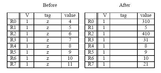
-
Complete the five instruction sequence in program order in the space below. Note that we have helped you by giving you the opcode and two source operand addresses for instruction 4. (The program sequence is unique.)

-
In cycle 1 instruction 1 is fetched. In cycle 2, instruction 1 is decoded and instruction 2 is fetched. In cycle 3, instruction 1 starts execution, instruction 2 is decoded, and instruction 3 is fetched.
Assume the reservation stations are all initially empty. Put each instruction into the next available reservation station. For example, the first ADD goes into “a”. The first MUL goes into “x”. Instructions remain in the reservation stations until they are completed. Show the state of the reservation stations at the end of cycle 8.
Note: to make it easier for the grader, when allocating source registers to reservation stations, please always have the higher numbered register be assigned to SR2.

-
Show the state of the Register Alias Table (V, tag, Value) at the end of cycle 8.
