The following program computes the square (k*k) of a positive integer k, stored
in location 0x4000 and stores the result in location 0x4002.
The result is to be treated as a 16-bit unsigned number.
Assumptions:
- A memory access takes 5 cycles
- The system call initiated by the
HALTinstruction takes 20 cycles to execute. This does not include the number of cycles it takes to execute theHALTinstruction itself.
        .ORIG X3000
        AND R0, R0, #0
        LEA R3, NUM
        LDW R3, R3, #0
        LDW R1, R3, #0
        ADD R2, R1, #0
LOOP    ADD R0, R0, R1
        ADD R2, R2, #-1
        BRP LOOP
        STW R0, R3, #1
        HALT
NUM     .FILL x4000
.END- How many cycles does each instruction take to execute on the LC-3b microarchitecture described in Appendix C?
- How many cycles does the entire program take to execute? (answer in terms of k)
- What is the maximum value of k for which this program still works correctly?
- How will you modify this program to support negative values of k? Explain in less than 30 words.
- What is the new range of k?
- In which state(s) in the LC-3b state diagram should the
LD.BENsignal be asserted? Is there a way for the LC-3b to work correctly without theLD.BENsignal? Explain. - Suppose we want to get rid of the
BENregister altogether. Can this be done? If so, explain how. If not, why not? Is it a good idea? Explain. - Suppose we took this further and wanted to get rid of state 0. We can do this by
modifying the microsequencer, as shown in the figure below. What is the 4-bit signal
denoted as
Ain the figure? What is the 1-bit signal denoted asB?

We wish to use the unused opcode “1010” to implement a new instruction ADDM, which (similar
to an IA-32 instruction) adds the contents of a memory location to either the contents of a
register or an immediate value and stores the result into a register. The specification of this instruction is as follows:
Assembler Formats
ADDM DR, SR1, SR2ADDM DR, SR1, imm5
Encodings

Operation
if (bit[5] == 0)
    DR = Memory[SR1] + SR2;
else
    DR = Memory[SR1] + SEXT(imm5);
setcc(DR);
We show below an addition to the state diagram necessary to implement
ADDM. Using the notation of the LC-3b State Diagram, describe inside each “bubble” what happens in each state, and assign each state an appropriate state number (stateAhas been done for you). Also, what is the one-bit signal denoted asXin the figure? Note: Be sure your solution works when the same register is used for both sources and the destination (eg.,ADDM R1, R1, R1).
Add to the Data Path any additional structures and any additional control signals needed to implement
ADDM. Label the additional control signalsECS 1(for “extra control signal 1”),ECS 2, etc.The processing in each state
A,B,C,Dis controlled by asserting or negating each control signal. Enter a 1 or a 0 as appropriate for the microinstructions corresponding to statesA,B,C,D.

The Address Control Logic in the LC-3b datapath of Figure C.3 in Appendix C allows the LC-3b to support memory-mapped I/O. There are three inputs to this logic:
- 16-bit address in
MAR. This signal can take the following values:xFE00,xFE02,xFE04,xFE06, andOTHER(any other address betweenx0000andxFDFF). - 1-bit
controlsignalR.. The access is a read access if this signal isWR, write access if it isW. - 1-bit control signal
MIO.EN. If this signal is 1, a memory or I/O access should be performed in this cycle.
The logic has five outputs:
- 1-bit
MEM.ENsignal. Memory is enabled if this signal is 1. - 2-bit select signal for
INMUX. This signal can take the following values:KBDR,KBSR,DSR,MEMORY. - 1-bit
LD.KBSRsignal.KBSRwill be load-enabled at the end of the current cycle if this signal is 1. - 1-bit
LD.DDRsignal.DDRwill be load-enabled at the end of the current cycle if this signal is 1. - 1-bit
LD.DSRsignal.DSRwill be load-enabled at the end of the current cycle if this signal is 1.
Your task is to draw the truth table for this Address Control Logic. Mark don't care values with “X” in your truth table. Use the conventions described above to denote the values of inputs and outputs. Please read Section C.6 in Appendix C on memory-mapped I/O before answering this question. Also, refer to Appendix A to find out the addresses of device registers.
The LC-3b state diagram handed out in class contained errors in states 4, 20, and 21. We have posted both versions of the handout: wrong and corrected. Briefly explain the problem we have corrected.
Answer the following short questions:
A memory's addressability is 64 bits. What does that tell you about the sizes of the MAR and the MDR?
We want to increase the number of registers that we can specify in the LC-3b ADD instruction to 32. Do you see any problem with that? Explain.
Given the following code:
MUL R3, R1, R2
ADD R5, R4, R3
ADD R6, R4, R1
MUL R7, R8, R9
ADD R4, R3, R7
MUL R10, R5, R6
Note: Each instruction is specified with the destination register first.
Calculate the number of cycles it takes to execute the given code on the following models:
- A non-pipelined machine.
- A pipelined machine with scoreboarding and five adders and five multipliers.
- A pipelined machine with scoreboarding and one adder and one multiplier.
Note: For all machine models, use the basic instruction cycle as follows:
- Fetch (one clock cycle)
- Decode (one clock cycle)
- Execute (MUL takes 6, ADD takes 4 clock cycles). The multiplier and the adder are not pipelined.
- Write-back (one clock cycle)
Do not forget to list any assumptions you make about the pipeline structure (e.g., data forwarding between pipeline stages). Infact, we encourage you to solve the above mentioned questions with data forwarding as well, but, you are not required to do so.
Suppose we have the following loop executing on a pipelined LC-3b machine.
DOIT     STW   R1, R6, #0
         ADD   R6, R6, #2
         AND   R3, R1, R2
         BRz   EVEN
         ADD   R1, R1, #3
         ADD   R5, R5, #-1
         BRp   DOIT
EVEN     ADD   R1, R1, #1
         ADD   R7, R7, #-1
         BRp   DOIT
Assume that before the loop starts, the registers have the following decimal values stored in them:
| Register | Value |
|---|---|
| R0 | 0 |
| R1 | 0 |
| R2 | 1 |
| R3 | 0 |
| R4 | 0 |
| R5 | 5 |
| R6 | 4000 |
| R7 | 5 |
The fetch stage takes one cycle, the decode stage also takes one cycle, the execute stage takes a variable number of cycles depending on the type of instruction (see below), and the store stage takes one cycle.
All execution units (including the load/store unit) are fully pipelined and the following instructions that use these units take the indicated number of cycles:
| Instruction | Number of Cycles |
|---|---|
| STW | 3 |
| ADD | 3 |
| AND | 2 |
| BR | 1 |
Data forwarding is used wherever possible. Instructions that are dependent on the previous instructions can make use of the results produced right after the previous instruction finishes the execute stage.
The target instruction after a branch can be fetched when the BR instruction is in ST stage. For example, the execution of an ADD instruction followed by a BR would look like:
ADD       F | D | E1 | E2 | E3 | ST
BR            F | D  | -  | -  | E1 | ST
TARGET                                F  | D
The pipeline implements “in-order execution.” A scoreboarding scheme is used as discussed in class.
Answer the following questions:
How many cycles does the above loop take to execute if no branch prediction is used?
How many cycles does the above loop take to execute if all branches are predicted with 100% accuracy.
How many cycles does the above loop take to execute if a static BTFN (backward taken-forward not taken) branch prediction scheme is used to predict branch directions? What is the overall branch prediction accuracy? What is the prediction accuracy for each branch?
A five instruction sequence executes according to Tomasulo's
algorithm. Each instruction is of the form ADD DR,SR1,SR2 or MUL
DR,SR1,SR2. ADDs are pipelined and take 9 cycles
(F-D-E1-E2-E3-E4-E5-E6-WB). MULs are also pipelined and take 11 cycles (two
extra execute stages). The microengine must wait until a result is in
a register before it sources it (reads it as a source operand).
The register file before and after the sequence are shown below (tags for “After” are ignored).

-
Complete the five instruction sequence in program order in the space below. Note that we have helped you by giving you the opcode and two source operand addresses for instruction 4. (The program sequence is unique.)

-
In cycle 1 instruction 1 is fetched. In cycle 2, instruction 1 is decoded and instruction 2 is fetched. In cycle 3, instruction 1 starts execution, instruction 2 is decoded, and instruction 3 is fetched.
Assume the reservation stations are all initially empty. Put each instruction into the next available reservation station. For example, the first ADD goes into “a”. The first MUL goes into “x”. Instructions remain in the reservation stations until they are completed. Show the state of the reservation stations at the end of cycle 8.
Note: to make it easier for the grader, when allocating source registers to reservation stations, please always have the higher numbered register be assigned to SR2.

-
Show the state of the Register Alias Table (V, tag, Value) at the end of cycle 8.

In class, we discussed the asynchronous finite state machine for the device controller of an input-output device within the context of a priority arbitration system. Draw the state diagram for this device controller (as drawn in lecture), identify the input and output signals, and briefly explain the function of each input and output signal.
As mentioned in class, the finite state machine has some race conditions. Identify the race conditions and show what simple modifications can be made to eliminate them.
In class we discussed asynchronous buses with central arbitration. Our job in this problem is to design the state machine for a synchronous bus using distributed arbitration. Recall that with distributed arbitration, each device receives the Bus Request signals from all other devices, and determines whether or not it is the next Bus Master. Assume all bus transactions take exactly one cycle, and that no device may be the Bus Master for two consecutive cycles.
Assume four devices, having priorities 1, 2, 3, and 4 respectively. Their respective controllers request the bus via asserting BR1, BR2, BR3, and BR4 respectively. Priority 4 is the highest priority.
-
Show the interconnections required for distributed arbitration for the four devices and their controllers connected to the bus. Be sure to label each signal line and designate by arrows whether the signals are input or output with respect to the device.
-
Is it possible for starvation to occur in this configuration? Describe the situation where this can occur.
-
Assume each I/O Controller is implemented using a clocked finite state machine. Draw a Moore model state machine for the controller operating at priority level 2. Label each state clearly. Label all necesary inputs and outputs. You do not need to show the clock signal on the state machine diagram. State transitions are synchronized to the clock.
Consider the following piece of code:
for(i = 0; i < 100; i++)
  A[i] = ((B[i] * C[i]) + D[i]) / 2;
Translate this code into assembly language using the following instructions in the ISA (note the number of cycles each instruction takes is shown with each instruction):
Opcode Operands Number of Cycles Description LEARi, X1 Ri ← address of X LDRi, Rj, Rk11 Ri ← MEM[Rj + Rk] STRi, Rj, Rk11 MEM[Rj + Rk] ← Ri MOVIRi, Imm1 Ri ← Imm MULRi, Rj, Rk6 Ri ← Rj × Rk ADDRi, Rj, Rk4 Ri ← Rj + Rk ADDRi, Rj, Imm4 Ri ← Rj + Imm RSHFARi, Rj, amount1 Ri ← RSHFA (Rj, amount) BRccX1 Branch to X based on condition codes Assume it takes one memory location to store each element of the array. Also assume that there are 8 registers (R0-R7).
How many cycles does it take to execute the program?
-
Now write Cray-like vector/assembly code to perform this operation in the shortest time possible. Assume that there are 8 vector registers and the length of each vector register is 64. Use the following instructions in the vector ISA:
Opcode Operands Number of Cycles Description LDVst, #n1 Vst ← n LDVln, #n1 Vln ← n VLDVi, X11, pipelined VSTVi, X11, pipelined VmulVi, Vj, Vk6, pipelined VaddVi, Vj, Vk4, pipelined VrshfaVi, Vj, amount1 VbrccX1 How many cycles does it take to execute the program on the following processors? Assume that memory is 16-way interleaved.
- Vector processor without chaining, 1 port to memory (1 load or store per cycle)
- Vector processor with chaining, 1 port to memory
- Vector processor with chaining, 2 read ports and 1 write port to memory
Little Computer Inc. is now planning to build a new computer that is more suited for scientific applications. LC-3b can be modified for such applications by replacing the data type Byte with Vector. The new computer will be called LmmVC-3 (Little 'mickey mouse' Vector Computer 3). Your job is to help us implement the datapath for LmmVC-3. LmmVC-3 ISA will support all the scalar operations that LC-3b currently supports except the LDB and STB will be replaced with VLD and VST respectively. Our datapath will need to support the following new instructions:
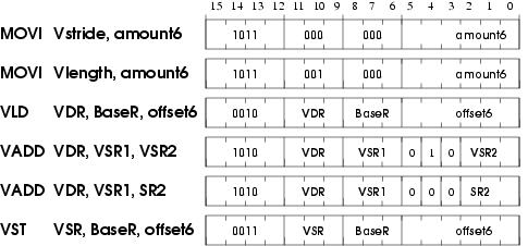
Note: VDR means “Vector Destination Register” and VSR means “Vector Source Register.”
- MOVI
- If IR[11:9] = 000, MOVI moves the unsigned quantity amount6 to Vector Stride Register (Vstride). If IR[11:9] = 001, MOVI moves the unsigned quantity amount6 to Vector Length Register (Vlength). This instruction has already been implemented for you.
- VLD
- VLD loads a vector of length Vlength from memory into VDR. VLD uses the opcode previously used by LDB. The starting address of the vector is computed by adding the LSHF1(SEXT(offset6)) to BaseR. Subsequent addresses are obtained by adding LSHF1(ZEXT(Vstride)) to the address of the preceding vector element.
- VST
- VST writes the contents of VSR into memory. VST uses the opcode previously used by STB. Address calculation is done in the same way as for VLD.
- VADD
- If IR[4] is a 1, VADD adds two vector registers (VSR1 and VSR2) and stores the result in VDR. If IR[4] is a 0, VADD adds a scalar register (SR2) to every element of VSR and stores the result in VDR.
VLD, VST, and VADD do not modify the content of Vstride and Vlength registers.
The following five hardware structures have been added to LC-3b in order to implement LmmVC-3.
- Vector Register File with eight 63-element Vector registers
- Vector Length Register
- Vector Stride Register
- A third input to DRMUX containing IR[8:6]
- Grey box A
- Box labeled X
These structures are shown in the LmmVC-3 datapath diagram:
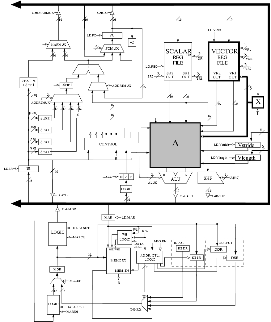
A 6-bit input to the Vector Register file has been labeled X on the datapath diagram. What is the purpose of this input? (Answer in less than 10 words )
The logic structure X contains a 6-bit register and some additional logic. X has two control signals as its inputs. What are these signals used for?
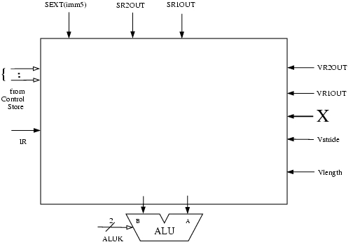
Grey box A contains several additional muxes on both input lines to the ALU. Complete the logic diagram of grey box A (shown below) by showing all muxes and interconnects. You will need to add new signals to the control store; be sure to clearly label them in the logic diagram.
- Keep in mind that we will still need to support all the existing scalar operations.
- The XOR operation in the ALU can be used to compare two values.
- Our solution required 3 additional control signals and 6 2-to-1 muxes.
-
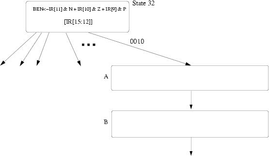
We show the beginning of the state diagram necessary to implement VLD. Using the notation of the LC-3b State Diagram, add the states you need to implement VLD. Inside each state describe what happens in that state. You can assume that you are allowed to make any changes to the microsequencer that you find necessary. You do not have to make/show these changes. You can modify BaseR and the condition codes. Make sure your design works when Vlength equals 0. Full credit will be awarded to solutions that require no more than 7 states.
Consider the following example used to explain Tomasulo's Algorithm:
Format: Opcode Destination Source1 Source2
MUL R3,  R1, R2
ADD R5,  R3, R4
ADD R7,  R2, R6
ADD R10, R8, R9
MUL R11, R7, R10
ADD R5,  R5, R11
MUL R10, R4, R10
Construct the Data Flow Graph for this program.