The ISA is the contract between the hardware and the software. The microarchitecture is a particular implementation of an ISA. Compiler does not need to know any information about the microarchitecture.
- ISA
- Microarchitecture
- ISA
- Microarchitecture
- ISA
- Microarchitecture/ISA
- ISA
- Microarchitecture
- Microarchitecture
- Microarchitecture
The first program causes x0004 to be stored in location x3000 when the assembled code is loaded into the memory. The second program causes x0004 to be stored in x3000 during the execution of the program.
The following table shows the classification of the LC-3b instructions into Operate, Data Movement and Control instructions.
| Instruction | Operate | Data Movement | Control |
|---|---|---|---|
| ADD | X | ||
| AND | X | ||
| BR | X | ||
| JMP/RET | X | ||
| JSR/JSRR | X | ||
| LDB | X | ||
| LDW | X | ||
| LEA | X | ||
| RTI | X | ||
| SHF | X | ||
| STB | X | ||
| STW | X | ||
| TRAP | X | ||
| XOR/NOT | X |
Both the second and the third instruction (never branch) can be used as a NOP. The first instruction (ADD) sets the condition codes based on the value in R1, therefore it is also not a NOP.
- The first option does not support either subroutine nesting or subroutine recursion.
- The second option supports subroutine nesting, but does not support recursion.
- The third option supports both subroutine nesting and subroutine recursion.
- Little endian: MEM[
x1000] + MEM[x1002] =x1A0E+x0C11=x261F - Big endian: MEM[
x1000] + MEM[x1002] =x0E1A+x110C=x1F26
- The memory consists of 228 addressable locations. 28 bits are required to uniquely address each location.
- The memory consists of 228 ÷ 23 = 225 addressable locations. 25 bits are required to address a location.
- The memory consists of 228 ÷ 27 = 221 addressable locations. 21 bits are required to address a location.
- Zero-address machine:
PUSH A
PUSH B
PUSH C
MUL
ADD
PUSH D
PUSH E
PUSH D
PUSH C
MUL
ADD
SUB
MUL
POP X
Advantages: Operate instructions only require an opcode so they can be encoded very densely.
Disadvantages: not flexible in terms of manipulating operands, more instructions required to write programs.
-
One-address machine:
LOAD B
MUL C
ADD A
STORE A
LOAD C
MUL D
ADD E
STORE E
LOAD D
SUB E
MUL A
STORE X
Advantages: only a single register required, fewer instructions compared to the stack machine.
Disadvantage: not as flexible as 2 or 3-address machines. We need instructions to move data to and from the accumulator (We don't need these in a 3-address machine that supports memory-to-memory operations).
-
Two-address machine:
MUL B, C ADD A, B MUL C, D ADD C, E SUB D, C MUL A, D SUB X, X ; these two instructions emulate a MOV X, A ADD X, A -
Three-address machine:
MUL X, B, C
ADD A, X, A
MUL X, D, C
ADD X, E, X
SUB X, D, X
MUL X, X, A
- 2 address machine.
- 4 registers
- Lets say you want
MOV R2, R1(R2 = R1):
orAND R2, #0 ADD R2, R1LEA TEMP ; Absolute address of TEMP in R0 ST R1, R0 LD R2, R0 .... .... TEMP .FILL xDEAD ; any garbage value - Use the LEA instruction:
	LEA LABEL
	BR  R0
	....
LABEL	....	; Branch to this line
-
Symbol Address AGAIN x300E NO x3022 B x3024 A x3026 - If the high and low byte of the word stored at location x4000 are equal, R5 is set to 1, else to 0.
-
There are several possible answers to this code
optimization question. Some of these are:
-
The programmer used a loop to left shift a value
in R2 by 8 bits. He/she could have done this using a single LC-3b
instruction, LSHF. He/she should have replaced the loop
AGAIN ADD R2, R2, R2 ADD R3, R3, #-1 BRp AGAINwithLSHF R2, R2, #8
-
Instead of using "subtraction" to compare the high and low byte, the
programmer could have used a single XOR instruction to check the
equality of the two bytes. He/she could have replaced the following
instructions
        NOT R1, R1
	     ADD R1, R1, #1
	     ADD R2, R2, R1
withXOR R2, R1, R2
-
The program is comparing the high byte and low byte of the word in
memory location x4000. The programmer could have utilized the LDB
instruction to load the high byte and low byte into two separate
registers and compare them. This way there would be no need for
shifting and masking. The optimized program could look like this:
        .ORIG   x3000
	AND     R5, R5, #0
	LEA	R0, A
	LDW	R0, R0, #0
	LDB	R1, R0, #0
	LDB	R2, R0, #1
	XOR	R2, R1, R2
	BRnp    NO
	ADD     R5, R5, #1
NO	HALT
A       .FILL   x4000
        .END
-
The programmer used a loop to left shift a value
in R2 by 8 bits. He/she could have done this using a single LC-3b
instruction, LSHF. He/she should have replaced the loop
	.ORIG	x4000
MAIN	LEA	R2,L0
	JSRR	R2
	JSR	L1
	HALT
	;
L0	ADD	R0,R0,#5
	RET
	;
L1	ADD	R1,R1,#5
	RET
x4000	xE403
x4002	x4080
x4004	x4803
x4006	xF025

x4008	x1025
x400A	xC1C0

x400C	x1265
x400E xC1C0-
As long as the subroutine we are calling is located at most
1023 instructions before the JSR instruction or at most 1024
instructions after the JSR instruction, there is no need to use the
first way, which requires at least two instructions. This is due to
the fact that JSR instruction can change the PC to an address within
the range PC + 2 - 2048 and PC + 2 + 2046, because it uses a limited
offset of 11 bits.
The method that requires two instructions is necessary if the subroutine we are calling is not within the range of the JSR instruction. Note that the JSRR instruction can change the PC to any address residing in its base register. The address in the base register can be set to any address in memory.
For example if we have a program starting at memory location x3000 and we would like to call a subroutine starting at memory location 0xF000, there is no way to do this by just using a JSR instruction at location x3000. However, we can call the subroutine at 0xF000 using JSRR with the following sequence of instructions:
           .ORIG      x3000
           LEA        R0, SUBADDR
           LDW        R1, R0, #0
           JSRR	      R1
           HALT
SUBADDR    .FILL      xF000
           .END
Yes, there is a difference. The program at x5000 does not save the return address from the subroutine at L2 because it uses a JMP instruction. Thus, that program will not work correctly.
A possible change that could be made:
      .ORIG x5000
      LEA   R7,B
MAIN2 LEA   R3,L2
A2    JMP   R3
B     HALT
      ;
L2    ADD   R2,R1,R0
      RET
Possible Solutions:
-
4 opcode bits, 3 NZP bits, 3 DR bits, 3 SR1 bits, 3 SR2 bits
-
A 2 address operation can be used instead of a 3 address. Thus, we have 4 opcode bits, 3 NZP bits, 3 DR/SR1 bits, 1 steering bit. The remaining 5 bits will either be used as 5 immediate bits, or 2 unused bits + 3 SR2 bits.
Variable instruction length ISAs have more complex decode logic. Variable instruction length ISA programs can be encoded more densely. Variable instruction length ISAs also generally imply a richer instruction set than that of a fixed length ISA. Since a richer instruction set has more instructions that directly correspond to higher level language programming constructs, the compilation process can be easier.
The comments indicate the number of cycles each instruction takes:
        .ORIG X3000
AND R0, R0, #0    ; 9 cycles
        LEA R3, NUM       ; 9 cycles
        LDW R3, R3, #0    ; 15 cycles
        LDW R1, R3, #0    ; 15 cycles
        ADD R2, R1, #0    ; 9 cycles
LOOP    ADD R0, R0, R1    ; 9 cycles
        ADD R2, R2, #-1   ; 9 cycles
        BRP LOOP          ; 10 cycles for Taken / 9 for Not Taken
        STW R0, R3, #1    ; 15 cycles
        HALT              ; 35 cycles
NUM     .FILL x4000
        .END
To calculate the square of k, the inner loop gets executed k times. The branch is taken (k-1) times and not taken one time.
Number of cycles = 9 + 9 + 15 + 15 + 9 + (k-1)*(9 + 9 + 10) + 1*(9 + 9 + 9) + 15 + 35 = 28k + 106- k = 255
After we load the value of k, check if it is negative. If so, take the 2's complement before entering the loop.
k can range from -255 to +255
State 32. We can get rid of the LD_BEN signal altogether and always load enable the BEN register.
The value that is loaded into BEN in state 32 could instead be calculated in state 0, but this would add delay for calculating the next state and would probably force the cycle time to be increased.
-
A = IR[15:12]
B = IR[11]&N + IR[10]&Z + IR[9]&P  (i.e., the old BEN signal)
Filled in state sequence:
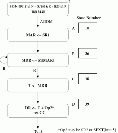
There are many possible state numberings, but state numbers must be chosen from 24, 34, and 36-63. The state number for C must differ from the state number for B only in the bit1 position, and bit1 must be 0 for state B. For example, if state B is 36 (100100), state C must be 38 (100110). The one-bit signal X is the Ready bit (R) from memory.
We need a 16-bit temporary register (T) which gets its inputs from the system bus. We need a signal LD.T (extra control signal 1) to control when to load this register. This register holds the data that is fetched from memory. We also need a mux in front of the A input of the ALU. This mux should select between SR1 and the output of the temporary register. We need a control signal for the select line of this mux (ALUMX2 - extra control signal 2).
ALUMX2 = 0 selects SR1
ALUMX2 = 1 selects TFilled in microinstructions:
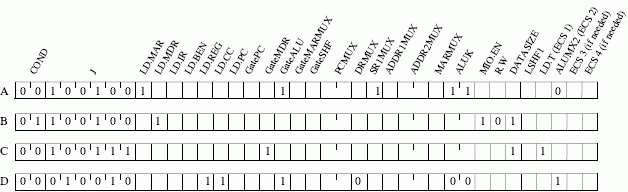
All other signals are 0. The J bits will depend on the state numbering chosen in part (a). The J bits for states A and B must correspond to the state number for B, the J bits for state C must correspond to the state number for D, and the J bits for D must be 18 (010010). The bit encodings for control signals are the same as specified in Lab 3.
Truth table for the Address Control Logic:
| MIO.EN | R.W | MAR | MEM.EN | INMUX | LD.KBSR | LD.DSR | LD.DDR |
|---|---|---|---|---|---|---|---|
| 0 | X | X | 0 | X | 0 | 0 | 0 |
| 1 | R | xFE00 |
0 | KBSR | 0 | 0 | 0 |
| 1 | R | xFE02 |
0 | KBDR | 0 | 0 | 0 |
| 1 | R | xFE04 |
0 | DSR | 0 | 0 | 0 |
| 1 | R | xFE06 |
0 | X | 0 | 0 | 0 |
| 1 | R | OTHER | 1 | MEMORY | 0 | 0 | 0 |
| 1 | W | xFE00 |
0 | X | 1 | 0 | 0 |
| 1 | W | xFE02 |
0 | X | 0 | 0 | 0 |
| 1 | W | xFE04 |
0 | X | 0 | 1 | 0 |
| 1 | W | xFE06 |
0 | X | 0 | 0 | 1 |
| 1 | W | OTHER | 1 | X | 0 | 0 | 0 |
In the wrong version, instructions JSR R7 and JSRR R7 would execute incorrectly. Their base register (R7) would be overwritten with the value of the PC in state 4. Thus, the addresses generated in states 20 and 21 would come out wrong.
We cannot tell the size of the MAR, since it depends on the number of memory locations and does not depend on the addressability (the number of bits in each location). For the MDR, first consider the LC3b. The LC3b is Byte (8 bit) addressable with an MDR size of 16 bits. We cannot tell the size of the MDR based on addressability either.
Each register (DR, SR1, and SR2) would have to be specified with five bits. With the steering bit, the total number of bits used would be 16 – leaving no bits for the opcode.