Given the following code:
MUL R3, R1, R2
ADD R5, R4, R3
ADD R6, R4, R1
MUL R7, R8, R9
ADD R4, R3, R7
MUL R10, R5, R6
Note: Each instruction is specified with the destination register first.
Calculate the number of cycles it takes to execute the given code on the following models:
- A non-pipelined machine.
- A pipelined machine with scoreboarding and five adders and five multipliers.
- A pipelined machine with scoreboarding and one adder and one multiplier.
Note: For all machine models, use the basic instruction cycle as follows:
- Fetch (one clock cycle)
- Decode (one clock cycle)
- Execute (MUL takes 6, ADD takes 4 clock cycles). The multiplier and the adder are not pipelined.
- Write-back (one clock cycle)
Do not forget to list any assumptions you make about the pipeline structure (e.g., data forwarding between pipeline stages). Infact, we encourage you to solve the above mentioned questions with data forwarding as well, but, you are not required to do so.
Suppose we have the following loop executing on a pipelined LC-3b machine.
DOIT     STW   R1, R6, #0
         ADD   R6, R6, #2
         AND   R3, R1, R2
         BRz   EVEN
         ADD   R1, R1, #3
         ADD   R5, R5, #-1
         BRp   DOIT
EVEN     ADD   R1, R1, #1
         ADD   R7, R7, #-1
         BRp   DOIT
Assume that before the loop starts, the registers have the following decimal values stored in them:
| Register | Value |
|---|---|
| R0 | 0 |
| R1 | 0 |
| R2 | 1 |
| R3 | 0 |
| R4 | 0 |
| R5 | 5 |
| R6 | 4000 |
| R7 | 5 |
The fetch stage takes one cycle, the decode stage also takes one cycle, the execute stage takes a variable number of cycles depending on the type of instruction (see below), and the store stage takes one cycle.
All execution units (including the load/store unit) are fully pipelined and the following instructions that use these units take the indicated number of cycles:
| Instruction | Number of Cycles |
|---|---|
| STW | 3 |
| ADD | 3 |
| AND | 2 |
| BR | 1 |
Data forwarding is used wherever possible. Instructions that are dependent on the previous instructions can make use of the results produced right after the previous instruction finishes the execute stage.
The target instruction after a branch can be fetched when the BR instruction is in ST stage. For example, the execution of an ADD instruction followed by a BR would look like:
ADD       F | D | E1 | E2 | E3 | ST
BR            F | D  | -  | -  | E1 | ST
TARGET                                F  | D
The pipeline implements “in-order execution.” A scoreboarding scheme is used as discussed in class.
Answer the following questions:
How many cycles does the above loop take to execute if no branch prediction is used?
How many cycles does the above loop take to execute if all branches are predicted with 100% accuracy.
How many cycles does the above loop take to execute if a static BTFN (backward taken-forward not taken) branch prediction scheme is used to predict branch directions? What is the overall branch prediction accuracy? What is the prediction accuracy for each branch?
Design the “WE Logic” block of the LC-3b datapath as shown on Figure C.3 in Appendix C.
The inputs to the block are MAR[0], R.W, and DATA.SIZE. The outputs of the block are WE0 and WE1.
Show the truth table for this logic block and give a gate-level implementation.
Consider the following piece of code:
     for(i = 0; i < 8; ++i){
       for(j = 0; j < 8; ++j){
         sum = sum + A[i][j];
       }
     }
The figure below shows an 8-way interleaved, byte-addressable memory. The total size of the memory is 4KB. The elements of the 2-dimensional array, A, are 4-bytes in length and are stored in the memory in column-major order (i.e., columns of A are stored in consecutive memory locations) as shown. The width of the bus is 32 bits, and each memory access takes 10 cycles.
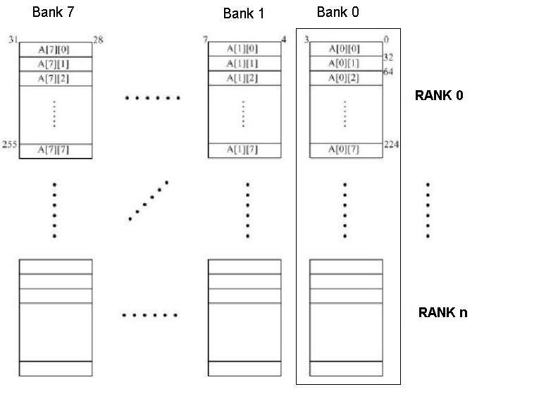
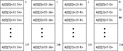
A more detailed picture of the memory chips in Rank 0 of Bank 0 is shown below.
Since the address space of the memory is 4KB, 12 bits are needed to uniquely identify each memory location, i.e.,
Addr[11:0]. Specify which bits of the address will be used for:- Byte on bus
Addr[_____:_____]
- Interleave bits
Addr[_____:_____]
- Chip address
Addr[_____:_____]
- Rank bits
Addr[_____:_____]
- Byte on bus
How many cycles are spent accessing memory during the execution of the above code? Compare this with the number of memory access cycles it would take if the memory were not interleaved (i.e., a single 4-byte wide array).
Can any change be made to the current interleaving scheme to optimize the number of cycles spent accessing memory? If yes, which bits of the address will be used to specify the byte on bus, interleaving, etc. (use the same format as in part a)? With the new interleaving scheme, how many cycles are spent accessing memory? Remember that the elements of A will still be stored in column-major order.
Using the original interleaving scheme, what small changes can be made to the piece of code to optimize the number of cycles spent accessing memory? How many cycles are spent accessing memory using the modified code?
The figure below illustrates the logic and
memory to support 512 MB (byte addressable) of physical memory, supporting
unaligned accesses. The ISA contains LDByte, LDHalfWord, LDWord,
STByte , STHalfWord and STWord instructions, where a word is 32 bits. Bit 28
serves as a chip enable (active high). If this bit is high the data of the
memory is loaded on the bus, otherwise the output of the memory chip floats (tri-stated).
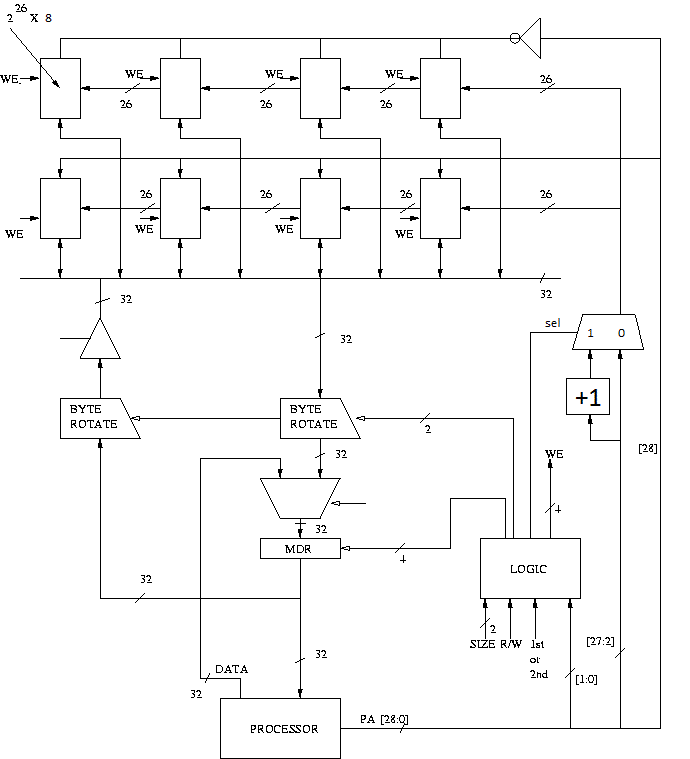
Note: the byte rotators in the figure are right rotators.
Construct the truth table to implement the LOGIC block, having inputs SIZE, R/W,
1st or 2nd access, PHYS_ADDR[1:0] and the outputs shown in the above figure. Assume
that the value of SIZE can be Byte (00), HalfWord (01), and Word (10). Clearly
explain what function each output serves.
If the latency of a DRAM memory bank is 37 cycles, into how many banks would you interleave this memory in order to fully hide this latency when making sequential memory accesses?
A bit-serial transmitter-receiver system operates at 1 GHz. It appends an even parity bit after every eight bits processed, as described in class. Therefore, for each byte of data, it transmits a nine bit message. Since the system is bit-serial, one message bit is transmitted each cycle. Assume that the probability of a bit being flipped while it is being transmitted is 10-7. In your solution, treat bit flips as statistically independent events.
What is the probability that a transmitted nine bit message will have one or more flipped bits? Hint: what is the probability that a transmitted nine bit message will have zero flipped bits?
If the parity check logic in the receiver detects an error in a message, how many bits may have been flipped in that message? (1, 2, 3, 4, 5, 6, 7, 8, 9 � circle all that apply).
If the parity check logic in the receiver does not detect an error in a message, how many bits may have been flipped in that message? (1, 2, 3, 4, 5, 6, 7, 8, 9 � circle all that apply).
What is the probability that a transmitted nine bit message will have exactly:
- 1 bit flipped
- 2 bits flipped
- 3 bits flipped
Notice that the probability of exactly three bits being flipped is negligible compared to the probabilities of one or two bits being flipped. Thus, for the rest of this problem, you may neglect the probabilities of three or more bits being flipped in one message.
- On average, how many detected bit errors per second will occur in the system?
- On average, how many undetected bit errors per second will occur in the system?
Note: this course is not about probability theory, and the undergraduate probability course (EE351K) is not a prerequisite. Thus, if you have difficulty solving this problem, please see one of the TA's.
An ISA supports an 8-bit, byte-addressable virtual address space. The corresponding physical memory has only 128 bytes. Each page contains 16 bytes. A simple, one-level translation scheme is used and the page table resides in physical memory. The initial contents of the frames of physical memory are shown below.
| Frame Number | Frame Contents |
|---|---|
| 0 | empty |
| 1 | Page 13 |
| 2 | Page 5 |
| 3 | Page 2 |
| 4 | empty |
| 5 | Page 0 |
| 6 | empty |
| 7 | Page Table |
A three-entry Translation Lookaside Buffer that uses LRU replacement is added to this system. Initially, this TLB contains the entries for pages 0, 2, and 13. For the following sequence of references, put a circle around those that generate a TLB hit and put a rectangle around those that generate a page fault. What is the hit rate of the TLB for this sequence of references? (Note: LRU policy is used to select pages for replacement in physical memory.)
References (to pages): 0, 13, 5, 2, 14, 14, 13, 6, 6, 13, 15, 14, 15, 13, 4, 3.
- At the end of this sequence, what three entries are contained in the TLB?
- What are the contents of the 8 physical frames?
We have been referring to the LC-3b memory as 2^16 bytes of memory, byte-addressable. This is the memory that the user sees, and may bear no relationship to the actual physical memory. Suppose that the actual physical address space is 8K bytes, and our page size is 512 bytes. What is the size of the PFN? Suppose we have a virtual memory system in which virtual memory is divided into User Space and System Space, and System Page Table remains resident in physical memory. System space includes trap vector table, interrupt vector table, operating system and supervisor stack as shown in Figure A.1 in Appendix A. The rest of the address space in Figure A.1 is user space. If each PTE contained, in addition to the PFN, a Valid bit, a modified bit, and two bits of access control, how many bits of physical memory would be required to store the System Page Table?
A little-endian machine with 64KB, byte addressable virtual memory and 4KB physical memory has two-level virtual address translation similar to the VAX. The page size of this machine is 256 bytes. Virtual address space is partitioned into the P0 space, P1 space, system space and reserved space. The space a virtual address belongs to is specified by the most significant two bits of the virtual address, with 00 indicating P0 space, 01 indicating P1 space, and 10 indicating system space. Assume that the PTE is 32 bits and contains only the Valid bit and the PFN in the format V0000000..000PFN.
For a single load instruction the physical memory was accessed three
times, excluding instruction fetch. The
first access was at location x108 and the value read from
that location (x10B,x10A,x109,x108) was x80000004. Hint: What does
this value mean?
The second access was at location x45C and the third access was at
location x942.
If SBR = x100, P0BR = x8250 and P1BR = x8350,
- What is the virtual address corresponding to physical address
x45C? - What is 32 bit value read from location
x45C? - What is the virtual address corresponding to physical address
x942?
Note: In this problem, the user and system virtual address spaces are not sized equally (the system virtual address space is 1/4 of the total virtual address space, and the user virtual address space makes up the other 3/4). Thus you need to include the address region bits in your calculation of the user space virtual page number. To make it easier for the machine to index into the user space page table, PTBR points to 0x380, which is at an offset of -0x20 from the actual first entry in the user space page table at 0x3A0. To index into the user space page table, add (user space virtual page number * PTE size) to the PTBR. (Why does this work?)
Consider a processor that supports a 9-bit physical address space with byte addressable memory. We would like the processor to support a virtual memory system. The features of the virtual memory system are:
    Virtual Memory Size : 4 Kbytes (12 bit address-space)
    Page Size           : 32 bytes
    PTBR                : 0x380
    SBR                 : 0x1E0
The virtual memory is divided into two spaces: system space and user space. System space is the first kilobyte of the virtual address space (i.e., most significant two bits of the virtual address are 00). The rest of the virtual memory is user space. The system page table remains resident in physical memory. Each PTE contains, in addition to the PFN, a Valid bit, a modified bit and 2 bits for access control. The format of the PTE is
| Valid | Modified | Access Control | PFN |
(Valid bit is the most significant bit of the PTE and the PFN is stored in the least significant bits.)
How many virtual pages does the system accommodate?
What is the size of the PFN? How big is the PTE?
How many bytes are required for storing the entire user space pagetable? How many pages does this correspond to?
-
Since the user space page table can occupy a significant portion of the the physical memory, this system uses a 2 level address translation scheme, by storing the user space Page Table in virtual memory (similar to VAX).
Given the virtual address 0x7AC what is the Physical address?
The following table shows the contents of the physical memory that you may need to do the translation:
Address Data x1F8xBAx1F9xBBx1FAxBCx1FBxBDx1FCxBEx1FDxB8x1FExB7x1FFxB6Address Data x118x81x119x72x11Ax65x11Bx34x11Cx97x11Dx83x11ExC6x11FxB2
The virtual address of variable X is x3456789A. Find the physical address
of X. Assume a Virtual Memory model similar to VAX.
Remember that in VAX each Virtual Address consists of:
- 2 bits to specify the Address Space
- 21 bits to specify Virtual Page Number
- 9 bits to specify the byte on the page
You will need to know the contents of P0BR: x8AC40000 and SBR: x000C8000.
You will also need to know the contents of the following physical memory locations:
x1EBA6EF0:    x80000A72
x0022D958:    x800F5D37
Some intermediate questions to help you:
- What virtual page of P0 Space is X on?
- What is VA of the PTE of the page containing X?
- What virtual page of System Space is this PTE on?
- What is the PA of the PTE of this page of System Space?
- What is the PA of the PTE of the page containing X?
An instruction is said to generate a page fault if a page fault occurs at any time during the processing of that instruction.
Let's say we added a virtual memory system to the LC-3b. Which instructions can possibly generate a page fault? What is the maximum number of page faults an instruction can possibly generate while it is being processed? Which instructions can possibly generate that maximum number of page faults? Assume that the virtual memory system added uses a one-level translation scheme and the page table is always resident in physical memory.
A computer has an 8KB write-through cache. Each cache block is 64 bits, the cache is 4-way set associative and uses a victim/next-victim pair of bits for each block for its replacement policy. Assume a 24-bit address space and byte-addressable memory. How big (in bits) is the tag store?
An LC-3b system ships with a two-way set associative, write back cache with perfect LRU replacement. The tag store requires a total of 4352 bits of storage. What is the block size of the cache? Please show all your work.
Hint: 4352 = 212 + 28.
Based on Hamacher et al., p. 255, question 5.18. You are working with a computer that has a first level cache that we call L1 and a second level cache that we call L2. Use the following information to answer the questions.
- The L1 hit rate is 0.95 for instruction references and 0.90 for data references.
- The L2 hit rate is 0.85 for instruction references and 0.75 for data references.
- 30% of all instructions are loads and stores.
- The size of each cache block is 8 words.
- The time needed to access a cache block in L1 is 1 cycle and the time needed to access a cache block in L2 is 6 cycles.
- The accesses to the caches and memory are done sequentially. If there is a miss in the L1 and a hit in the L2 then the total latency is 7 cycles.
- Memory is accessed only if there is a miss in both caches.
- The width of the memory bus is one word.
- It takes one clock cycle to send an address to main memory.
- It takes 20 cycles to access the main memory.
- It takes one cycle to send one word from the memory to the processor. Thus the total latency to get a word from memory to the processor is 22 cycles.
- The bus allows sending a new address to memory in the same cycle that data is sent from memory to the processor.
- Assume the data is accessible to the processor only AFTER the whole cache block has been brought in from the memory, and buffered on the processor chip. The processor can then access the data independent of and during the cache fill.
- What is the average access time per instruction (assume no interleaving)?
- What is the average access time per instruction if the main memory is 4-way interleaved?
- What is the average access time per instruction if the main memory is 8-way interleaved?
- What is the improvement obtained with interleaving?
Hamacher, pg.255, question 5.13. A byte-addressable computer has a small data cache capable of holding eight 32-bit words. Each cache block consists of one 32-bit word. When a given program is executed, the processor reads data from the following sequence of hex addresses:
200, 204, 208, 20C, 2F4, 2F0, 200, 204, 218, 21C, 24C, 2F4
This pattern is repeated four times.
-
Show the contents of the cache at the end of each pass throughout this loop if a direct-mapped cache is used. Compute the hit rate for this example. Assume that the cache is initially empty.
-
Repeat part (a) for a fully-associative cache that uses the LRU-replacement algorithm.
-
Repeat part (a) for a four-way set-associative cache that uses the LRU replacement algorithm.
Below, we have given you four different sequences of addresses generated by a program running on a processor with a data cache. Cache hit ratio for each sequence is also shown below. Assuming that the cache is initially empty at the beginning of each sequence, find out the following parameters of the processor's data cache:
- Associativity (1, 2, or 4 ways)
- Block size (1, 2, 4, 8, 16, or 32 bytes)
- Total cache size (256B, or 512B)
- Replacement policy (LRU or FIFO)
Assumptions: all memory accesses are one byte accesses. All addresses are byte addresses.
| Number | Address Sequence | Hit Ratio |
|---|---|---|
| 1 | 0, 2, 4, 8, 16, 32 | 0.33 |
| 2 | 0, 512, 1024, 1536, 2048, 1536, 1024, 512, 0 | 0.33 |
| 3 | 0, 64, 128, 256, 512, 256, 128, 64, 0 | 0.33 |
| 4 | 0, 512, 1024, 0, 1536, 0, 2048, 512 | 0.25 |