Chapter 8: Switch and LED Interfacing
Embedded Systems - Shape The World
Jonathan Valvano and Ramesh Yerraballi
We couldn’t wait to show you how much fun it is to make the microcontroller interact with real physical devices. So in this section we will take a short side step from the business of concepts and theories to teach you how to connect switches and LEDs to the microcontroller. We will use switches to input data and use LEDs to output results. In this chapter, we will illustrate the design, construction and testing of an embedded system. The switch LED and LaunchPad will then be combined to create a system. You will need a solid understanding of Ohm's Law, so you may need to review current, voltage, power, and resistance from Chapter 3.
Learning Objectives:
- Understanding basic circuit elements like source, ground, and resistors.
- Understanding how switches and LEDs work.
- Application of Ohm’s Law
- Analog circuit design and construction on a solderless breadboard
- Interfacing switches and LEDs to a microcontroller
- Programming simple logic.
Video 8.0. Circuit elements and Interfacing them to a Microcontroller
To build circuits, we’ll use a solderless breadboard, also referred to as a protoboard. The holes in the protoboard are internally connected in a systematic manner, as shown in Figure 8.1. The long rows of holes along the outer sides of the protoboard are electrically connected. Some protoboards like the one in Figure 8.1 have four long rows (two on each side), while others have just two long rows (one on each side). We refer to the long rows as power buses. If your protoboard has only two long rows (one on each side, we will connect one row to +3.3V and another row to ground. If your protoboard has two long rows on each side, then two rows will be ground, one row will be +3.3V. Use a black marker and label the voltage on each row. In the middle of the protoboard, you’ll find two groups of holes placed in a 0.1 inch grid. Each adjacent row of five pins is electrically connected. We usually insert components into these holes. If integrated circuits (IC) are to be placed on the protoboard, it is done such that the two rows of pins straddle the center valley.
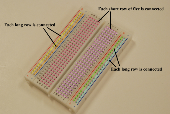
Figure 8.1. The pins on each of the four long rows are connected. The 5 pins in each short row are connected. Place a +3.3V wire to one long row. Place a ground wire from the LaunchPad to another long row.
To build a circuit we will use 22-gauge or 24-gauge solid wire. We strip off about 1/4 to 1/2 inch of insulation so the bare wire can be pushed straight into a hole. We only push one wire into a hole and remember which rows are internally connected as described in Figure 8.1.
Input/output devices are critical components of an embedded system. The first input device we will study is the switch. It allows the human to input binary information into the computer. Typically we define the asserted state, or logic true, when the switch is pressed. Contact switches can also be used in machines to detect mechanical contact (e.g., two parts touching, paper present in the printer, or wheels on the ground etc.) A single pole single throw (SPST) switch has two connections. The switches are shown as little open circles in Figure 8.2. In a normally open switch (NO), the resistance between the connections is infinite (over 100 MΩ on the B3F tactile switch) if the switch is not pressed and zero (under 0.1 Ω on the B3F tactile switch) if the switch is pressed.
<
Video 8.1. B3F Switch Datasheet
Video 8.2. Circuit for Switch Interface
To convert the infinite/zero resistance into a digital signal, we can use a pull-down resistor to ground or a pull-up resistor to +3.3V as shown in Figure 8.2. Notice that 10 kΩ is 100,000 times larger than the on-resistance of the switch and 10,000 times smaller than its off-resistance. Another way to choose the pull-down or pull-up resistor is to consider the input current of the microcontroller input pin. The current into the microcontroller will be less than 2µA (shown as IIL and IIH in the data sheet). So, if the current into microcontroller is 2µA, then the voltage drop across the 10 kΩ resistor will be 0.02 V, which is negligibly small. With a pull-down resistor, the digital signal will be low if the switch is not pressed and high if the switch is pressed (right Figure 8.2). This is defined as positive logic because the asserted state is a logic high. Conversely, with a pull-up resistor, the digital signal will be high if the switch is not pressed and low if the switch is pressed (middle of Figure 8.2). This is defined as negative logic because the asserted state is a logic low.

Figure 8.2. Single Pole Single Throw (SPST) Switch interface.
One of the complicating issues with mechanical switches is they can bounce (oscillate on and off) when touched and when released. The contact bounce varies from switch to switch and from time to time, but usually bouncing is a transient event lasting less than 5 ms. We can eliminate the effect of bounce if we design software that waits at least 10 ms between times we read the switch values.
To interface a switch we connect it to a pin (e.g., Figure 8.3) and initialize the pin as an input. The initialization function will enable the clock, set the direction register to input, turn off the alternative function, and enable the pin. Notice the software is friendly because it just affects PA5 without affecting the other bits in Port A. The input function reads Port A and returns a true (0x20) if the switch is pressed and returns a false (0) if the switch is not pressed. Figure 8.4 shows how we could build this circuit with a protoboard and a LaunchPad.

Figure 8.3. Interface of a switch to a microcomputer input.
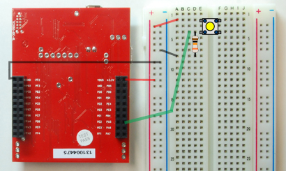
Figure 8.4. Construction of the interface of a switch to a microcomputer input. The brown-black-orange resistor is 10k. The switches in the lab-kit should plug into the protoboard. The switch is across the two pins that are closer to each other. It doesn't matter what color the wires are, but in this figure the wires are black, red and green. The two black wires are ground, the red wire is +3.3V, and the green wire is the signal in, which connects the switch to PA5 of the microcontroller.
The software in Program 8.1 is called a driver, and it includes an initialization, which is called once, and a second function that can be called to read the current position of the switch. Writing software this way is called an abstraction, because it separates what the switch does (Init, On, Off) from how it works (PortA, bit 5, TM4C123). The first input function uses the bit-specific address to get just PA5, while the second reads the entire port and selects bit 5 using a logical AND.
#define PA5 (*((volatile unsigned long *)0x40004080))
void Switch_Init(void){ volatile unsigned long delay;
SYSCTL_RCGCGPIO_R |= 0x00000001; // 1) activate clock for Port A
delay = SYSCTL_RCGCGPIO_R; // allow time for clock to start
// 2) no need to unlock GPIO Port A
GPIO_PORTA_AMSEL_R &= ~0x20; // 3) disable analog on PA5
GPIO_PORTA_PCTL_R &= ~0x00F00000; // 4) PCTL GPIO on PA5
GPIO_PORTA_DIR_R &= ~0x20; // 5) direction PA5 input
GPIO_PORTA_AFSEL_R &= ~0x20; // 6) PA5 regular port function
GPIO_PORTA_DEN_R |= 0x20; // 7) enable PA5 digital port
}
unsigned long Switch_Input(void){
return PA5; // return 0x20(pressed) or 0(not pressed)
}
unsigned long Switch_Input2(void){
return (GPIO_PORTA_DATA_R&0x20); // 0x20(pressed) or 0(not pressed)
}
Program 8.1. Software interface for a switch on PA5 (C8_Switch).
Maintenance Tip: When interacting with just some of the bits of an I/O register it is better to modify just the bits of interest, leaving the other bits unchanged. In this way, the action of one piece of software does not undo the action of another piece.
A light emitting diode (LED) emits light when an electric current passes through it. LEDs have polarity, meaning current must pass from anode to cathode to activate. The anode is labelled a or + , and cathode is labelled k or -. The cathode is the short lead and there may be a slight flat spot on the body of round LEDs. Thus, the anode is the longer lead. The brightness of an LED depends on the applied electrical power (P=I*V). Since the LED voltage is approximately constant in the active region (see left side of Figure 8.5), we can establish the desired brightness by setting the current.

Figure 8.5. Positive logic LED interface (Lite-On LTL-10223W).
Video 8.3. LED Datasheet
Video 8.4. Circuit for LED Interface
: What resistor value in Figure 8.5 is needed if the desired LED operating point is 1.7V and 11 mA?
If the LED current is above 8 mA, we cannot connect it directly to the microcontroller because the high currents may damage the chip. Figure 8.5 shows two possible interface circuits we could use. In both circuits if the software makes its output high the LED will be on. If the software makes its output low the LED will be off (shown in Figure 8.5 with italics). When the software writes a logic 1 to the output port, the input to the 7405/PN2222 becomes high, output from the 7405/PN2222 becomes low, 10 mA travels through the LED, and the LED is on. When the software writes a logic 0 to the output port, the input to the 7405/PN2222 becomes low, output from the 7405/PN2222 floats (neither high nor low), no current travels through the LED, and the LED is dark. The value of the resistor is selected to establish the proper LED current. When active, the LED voltage will be about 2 V, and the power delivered to the LED will be controlled by its current. If the desired brightness requires an operating point of 1.9 V at 10 mA, then the resistor value should be

where Vd, Id is the desired LED operating point, and VOL is the output low voltage of the LED driver. If we use a standard resistor value of 100Ω in place of the 90Ω, then the current will be (3.3-1.9-0.5V)/100Ω, which is about 9 mA. This slightly lower current is usually acceptable.

Figure 8.6. Low current LED interface (Agilent HLMP-D150).
When the LED current is less than 8 mA, we can interface it directly to an output pin without using a driver. The LED shown in Figure 8.6a has an operating point of 1.7 V and 1 mA. For the positive logic interface (Figure 8.6b) we calculate the resistor value based on the desired LED voltage and current

where VOH is the output high voltage of the microcontroller output pin. Since VOH can vary from 2.4 to 3.3 V, it makes sense to choose a resistor from a measured value of VOH, rather than the minimum value of 2.4 V. Negative logic means the LED is activated when the software outputs a zero. For the negative logic interface (Figure 8.6c) we use a similar equation to determine the resistor value

where VOL is the output low voltage of the microcontroller output pin.
If we use a 1.2 kΩ in place of the 1.3 kΩ, then the current will be (3.3-1.6-0.4V)/1.2kΩ, which is about 1.08 mA. This slightly higher current is usually acceptable. If we use a standard resistor value of 1.5 kΩ in place of the 1.3 kΩ, then the current will be (3.3-1.6-0.4V)/1.5kΩ, which is about 0.87 mA. This slightly lower current is usually acceptable.
The software in Program 8.2 is called a driver, and it includes an initialization, which is called once, and two functions that can be called to turn on and off the LED. Writing software this way is called an abstraction, because it separates what the LED does (Init, On, Off) from how it works (PortA, TM4C123).
: What resistor value in of Figure 8.6 is needed if the desired LED operating point is 1.7V and 2 mA? Use the negative logic interface and, VOL of 0.4V.
void LED_Init(void){ volatile
unsigned long
delay;
SYSCTL_RCGCGPIO_R |=
0x01;
// 1)
activate clock for Port A
delay =
SYSCTL_RCGCGPIO_R;
// allow time for clock to start
// 2) no need to unlock PA2
GPIO_PORTA_PCTL_R &= ~0x00000F00; // 3) regular GPIO
GPIO_PORTA_AMSEL_R &=
~0x04;
// 4) disable analog function on PA2
GPIO_PORTA_DIR_R |=
0x04;
// 5) set
direction to output
GPIO_PORTA_AFSEL_R &=
~0x04;
// 6) regular port function
GPIO_PORTA_DEN_R |=
0x04;
// 7) enable
digital port
}
// Make PA2 high
void LED_On(void){
GPIO_PORTA_DATA_R |= 0x04;
}
// Make PA2 low
void LED_Off(void){
GPIO_PORTA_DATA_R &= ~0x04;
}
Program 8.2. Software interface for an LED on PF2
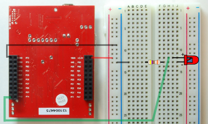
Figure 8.7. Construction of the interface of an LED to a microcomputer output (Figure 8.6b). The yellow-purple-brown resistor is 470ohm. It doesn't matter what color the wires are, but in this figure the wires are black, red and green. The two black wires are ground, the red wire is +3.3V, and the green wire is the signal Out, which connects PA2 of the microcontroller to the positive side of the LED.
Some problems are so unique that they require the engineer to invent completely original solutions. Most of the time, however, the engineer can solve even complex problems by building the system from components that already exist. Creativity will still be required in selecting the proper components, making small changes in their behavior (tweaking), arranging them in an effective and efficient manner, and then verifying the system satisfies both the requirements and constraints. When young engineers begin their first job, they are sometimes surprised to see that education does not stop with college graduation, but rather is a life-long activity. In fact, it is the educational goal of all engineers to continue to learn both processes (rules about how to solve problems) and products (hardware and software components). As the engineer becomes more experienced, he or she has a larger toolbox from which processes and components can be selected.
The hardest step for most new engineers is the first one: where to begin? We begin by analyzing the problem to create a set of specifications and constraints in the form of a requirements document. Next, we look for components, in the form of previously debugged solutions, which are similar to our needs. Often during the design process, additional questions or concerns arise. We at that point consult with our clients to clarify the problem. Next we rewrite the requirements document and get it reapproved by the clients.
It is often difficult to distinguish whether a parameter is a specification or a constraint. In actuality, when designing a system it often doesn’t matter into which category a parameter falls, because the system must satisfy all specifications and constraints. Nevertheless, when documenting the device it is better to categorize parameters properly. Specifications generally define in a quantitative manner the overall system objectives as given to us by our customers.
Constraints, on the other hand, generally define the boundary space within which we must search for a solution to the problem. If we must use a particular component, it is often considered a constraint. In this class, we constrain most designs to include a Tiva LaunchPad. Constraints also are often defined as an inequality, such as the cost must be less than $50, or the battery must last for at least one week. Specifications on the other hand are often defined as a quantitative number, and the system satisfies the requirement if the system operates within a specified tolerance of that parameter. Tolerance can be defined as a percentage error or as a range with minimum and maximum values.
In engineering everything is either a system or an interface between systems. For example a switch can be considered a system. When we interface it to the LaunchPad the switch-LaunchPad combination is a new system. Therefore, we begin by collecting the components required to build the system. We then combine the components and debug the system. As the components are combined we create new more powerful components. When writing software, we can use flowcharts to develop new algorithms. The more we can simulate the system, the more design possibilities we can evaluate, and the quicker we can make changes. Debugging involves both making sure it works, together with satisfying all requirements and constraints.
