Jonathan Valvano and Ramesh Yerraballi
Reprinted with approval from Introduction to Embedded Systems,
            ISBN: 978-1537105727 (8th printing,
        July 2021)  
Table of Contents:
 
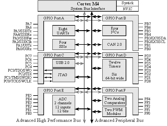
Figure 1.1. I/O port pins for the TM4C123GH6PM microcontroller.

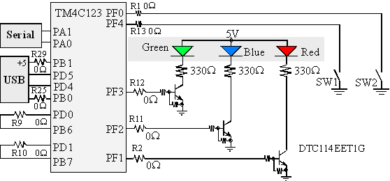
Figure 1.2. Switch and LED interfaces on the Tiva® LaunchPad Evaluation Board. The zero ohm resistors can be removed so the corresponding pin can be used for its regular purpose.

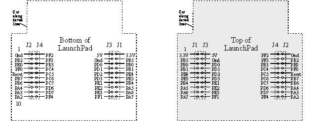
Figure 1.5. Pin locations on the LaunchPad.

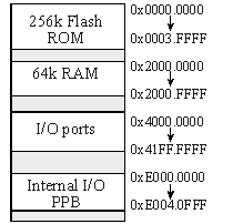
Figure 1.4. TM4C12address map.
| 
               Address  | 
            
               7  | 
            
               6  | 
            
               5  | 
            
               4  | 
            
               3  | 
            
               2  | 
            
               1  | 
            
               0  | 
            
               Name  | 
          
| 
               $400F.E608  | 
            
               
  | 
            
               
  | 
            
               GPIOF  | 
            
               GPIOE  | 
            
               GPIOD  | 
            
               GPIOC  | 
            
               GPIOB  | 
            
               GPIOA  | 
            
               SYSCTL_RCGCGPIO_R  | 
          
| 
               $4000.43FC  | 
            
               DATA  | 
            
               DATA  | 
            
               DATA  | 
            
               DATA  | 
            
               DATA  | 
            
               DATA  | 
            
               DATA  | 
            
               DATA  | 
            
               GPIO_PORTA_DATA_R  | 
          
| 
               $4000.4400  | 
            
               DIR  | 
            
               DIR  | 
            
               DIR  | 
            
               DIR  | 
            
               DIR  | 
            
               DIR  | 
            
               DIR  | 
            
               DIR  | 
            
               GPIO_PORTA_DIR_R  | 
          
| 
               $4000.4420  | 
            
               SEL  | 
            
               SEL  | 
            
               SEL  | 
            
               SEL  | 
            
               SEL  | 
            
               SEL  | 
            
               SEL  | 
            
               SEL  | 
            
               GPIO_PORTA_AFSEL_R  | 
          
| 
               $4000.4510  | 
            
               PUE  | 
            
               PUE  | 
            
               PUE  | 
            
               PUE  | 
            
               PUE  | 
            
               PUE  | 
            
               PUE  | 
            
               PUE  | 
            
               GPIO_PORTA_PUR_R  | 
          
| 
               $4000.451C  | 
            
               DEN  | 
            
               DEN  | 
            
               DEN  | 
            
               DEN  | 
            
               DEN  | 
            
               DEN  | 
            
               DEN  | 
            
               DEN  | 
            
               GPIO_PORTA_DEN_R  | 
          
| 
               $4000.4524  | 
            
               1  | 
            
               1  | 
            
               1  | 
            
               1  | 
            
               1  | 
            
               1  | 
            
               1  | 
            
               1  | 
            
               GPIO_PORTA_CR_R  | 
          
| 
               $4000.4528  | 
            
               0  | 
            
               0  | 
            
               0  | 
            
               0  | 
            
               0  | 
            
               0  | 
            
               0  | 
            
               0  | 
            
               GPIO_PORTA_AMSEL_R  | 
          
| 
               $4000.53FC  | 
            
               DATA  | 
            
               DATA  | 
            
               DATA  | 
            
               DATA  | 
            
               DATA  | 
            
               DATA  | 
            
               DATA  | 
            
               DATA  | 
            
               GPIO_PORTB_DATA_R  | 
          
| 
               $4000.5400  | 
            
               DIR  | 
            
               DIR  | 
            
               DIR  | 
            
               DIR  | 
            
               DIR  | 
            
               DIR  | 
            
               DIR  | 
            
               DIR  | 
            
               GPIO_PORTB_DIR_R  | 
          
| 
               $4000.5420  | 
            
               SEL  | 
            
               SEL  | 
            
               SEL  | 
            
               SEL  | 
            
               SEL  | 
            
               SEL  | 
            
               SEL  | 
            
               SEL  | 
            
               GPIO_PORTB_AFSEL_R  | 
          
| 
               $4000.5510  | 
            
               PUE  | 
            
               PUE  | 
            
               PUE  | 
            
               PUE  | 
            
               PUE  | 
            
               PUE  | 
            
               PUE  | 
            
               PUE  | 
            
               GPIO_PORTB_PUR_R  | 
          
| 
               $4000.551C  | 
            
               DEN  | 
            
               DEN  | 
            
               DEN  | 
            
               DEN  | 
            
               DEN  | 
            
               DEN  | 
            
               DEN  | 
            
               DEN  | 
            
               GPIO_PORTB_DEN_R  | 
          
| 
               $4000.5524  | 
            
               1  | 
            
               1  | 
            
               1  | 
            
               1  | 
            
               1  | 
            
               1  | 
            
               1  | 
            
               1  | 
            
               GPIO_PORTB_CR_R  | 
          
| 
               $4000.5528  | 
            
               0  | 
            
               0  | 
            
               AMSEL  | 
            
               AMSEL  | 
            
               0  | 
            
               0  | 
            
               0  | 
            
               0  | 
            
               GPIO_PORTB_AMSEL_R  | 
          
| 
               $4000.63FC  | 
            
               DATA  | 
            
               DATA  | 
            
               DATA  | 
            
               DATA  | 
            
               JTAG  | 
            
               JTAG  | 
            
               JTAG  | 
            
               JTAG  | 
            
               GPIO_PORTC_DATA_R  | 
          
| 
               $4000.6400  | 
            
               DIR  | 
            
               DIR  | 
            
               DIR  | 
            
               DIR  | 
            
               JTAG  | 
            
               JTAG  | 
            
               JTAG  | 
            
               JTAG  | 
            
               GPIO_PORTC_DIR_R  | 
          
| 
               $4000.6420  | 
            
               SEL  | 
            
               SEL  | 
            
               SEL  | 
            
               SEL  | 
            
               JTAG  | 
            
               JTAG  | 
            
               JTAG  | 
            
               JTAG  | 
            
               GPIO_PORTC_AFSEL_R  | 
          
| 
               $4000.6510  | 
            
               PUE  | 
            
               PUE  | 
            
               PUE  | 
            
               PUE  | 
            
               JTAG  | 
            
               JTAG  | 
            
               JTAG  | 
            
               JTAG  | 
            
               GPIO_PORTC_PUR_R  | 
          
| 
               $4000.651C  | 
            
               DEN  | 
            
               DEN  | 
            
               DEN  | 
            
               DEN  | 
            
               JTAG  | 
            
               JTAG  | 
            
               JTAG  | 
            
               JTAG  | 
            
               GPIO_PORTC_DEN_R  | 
          
| 
               $4000.6524  | 
            
               1  | 
            
               1  | 
            
               1  | 
            
               1  | 
            
               JTAG  | 
            
               JTAG  | 
            
               JTAG  | 
            
               JTAG  | 
            
               GPIO_PORTC_CR_R  | 
          
| 
               $4000.6528  | 
            
               AMSEL  | 
            
               AMSEL  | 
            
               AMSEL  | 
            
               AMSEL  | 
            
               JTAG  | 
            
               JTAG  | 
            
               JTAG  | 
            
               JTAG  | 
            
               GPIO_PORTC_AMSEL_R  | 
          
| 
               $4000.73FC  | 
            
               DATA  | 
            
               DATA  | 
            
               DATA  | 
            
               DATA  | 
            
               DATA  | 
            
               DATA  | 
            
               DATA  | 
            
               DATA  | 
            
               GPIO_PORTD_DATA_R  | 
          
| 
               $4000.7400  | 
            
               DIR  | 
            
               DIR  | 
            
               DIR  | 
            
               DIR  | 
            
               DIR  | 
            
               DIR  | 
            
               DIR  | 
            
               DIR  | 
            
               GPIO_PORTD_DIR_R  | 
          
| 
               $4000.7420  | 
            
               SEL  | 
            
               SEL  | 
            
               SEL  | 
            
               SEL  | 
            
               SEL  | 
            
               SEL  | 
            
               SEL  | 
            
               SEL  | 
            
               GPIO_PORTD_AFSEL_R  | 
          
| 
               $4000.7510  | 
            
               PUE  | 
            
               PUE  | 
            
               PUE  | 
            
               PUE  | 
            
               PUE  | 
            
               PUE  | 
            
               PUE  | 
            
               PUE  | 
            
               GPIO_PORTD_PUR_R  | 
          
| 
               $4000.751C  | 
            
               DEN  | 
            
               DEN  | 
            
               DEN  | 
            
               DEN  | 
            
               DEN  | 
            
               DEN  | 
            
               DEN  | 
            
               DEN  | 
            
               GPIO_PORTD_DEN_R  | 
          
| 
               $4000.7524  | 
            
               CR  | 
            
               1  | 
            
               1  | 
            
               1  | 
            
               1  | 
            
               1  | 
            
               1  | 
            
               1  | 
            
               GPIO_PORTD_CR_R  | 
          
| 
               $4000.7528  | 
            
               0  | 
            
               0  | 
            
               AMSEL  | 
            
               AMSEL  | 
            
               AMSEL  | 
            
               AMSEL  | 
            
               AMSEL  | 
            
               AMSEL  | 
            
               GPIO_PORTD_AMSEL_R  | 
          
| 
               $4002.43FC  | 
            
               
  | 
            
               
  | 
            
               DATA  | 
            
               DATA  | 
            
               DATA  | 
            
               DATA  | 
            
               DATA  | 
            
               DATA  | 
            
               GPIO_PORTE_DATA_R  | 
          
| 
               $4002.4400  | 
            
               
  | 
            
               
  | 
            
               DIR  | 
            
               DIR  | 
            
               DIR  | 
            
               DIR  | 
            
               DIR  | 
            
               DIR  | 
            
               GPIO_PORTE_DIR_R  | 
          
| 
               $4002.4420  | 
            
               
  | 
            
               
  | 
            
               SEL  | 
            
               SEL  | 
            
               SEL  | 
            
               SEL  | 
            
               SEL  | 
            
               SEL  | 
            
               GPIO_PORTE_AFSEL_R  | 
          
| 
               $4002.4510  | 
            
               
  | 
            
               
  | 
            
               PUE  | 
            
               PUE  | 
            
               PUE  | 
            
               PUE  | 
            
               PUE  | 
            
               PUE  | 
            
               GPIO_PORTE_PUR_R  | 
          
| 
               $4002.451C  | 
            
               
  | 
            
               
  | 
            
               DEN  | 
            
               DEN  | 
            
               DEN  | 
            
               DEN  | 
            
               DEN  | 
            
               DEN  | 
            
               GPIO_PORTE_DEN_R  | 
          
| 
               $4002.4524  | 
            
               
  | 
            
               
  | 
            
               1  | 
            
               1  | 
            
               1  | 
            
               1  | 
            
               1  | 
            
               1  | 
            
               GPIO_PORTE_CR_R  | 
          
| 
               $4002.4528  | 
            
               
  | 
            
               
  | 
            
               AMSEL  | 
            
               AMSEL  | 
            
               AMSEL  | 
            
               AMSEL  | 
            
               AMSEL  | 
            
               AMSEL  | 
            
               GPIO_PORTE_AMSEL_R  | 
          
| 
               $4002.53FC  | 
            
               
  | 
            
               
  | 
            
               
  | 
            
               DATA  | 
            
               DATA  | 
            
               DATA  | 
            
               DATA  | 
            
               DATA  | 
            
               GPIO_PORTF_DATA_R  | 
          
| 
               $4002.5400  | 
            
               
  | 
            
               
  | 
            
               
  | 
            
               DIR  | 
            
               DIR  | 
            
               DIR  | 
            
               DIR  | 
            
               DIR  | 
            
               GPIO_PORTF_DIR_R  | 
          
| 
               $4002.5420  | 
            
               
  | 
            
               
  | 
            
               
  | 
            
               SEL  | 
            
               SEL  | 
            
               SEL  | 
            
               SEL  | 
            
               SEL  | 
            
               GPIO_PORTF_AFSEL_R  | 
          
| 
               $4002.5510  | 
            
               
  | 
            
               
  | 
            
               
  | 
            
               PUE  | 
            
               PUE  | 
            
               PUE  | 
            
               PUE  | 
            
               PUE  | 
            
               GPIO_PORTF_PUR_R  | 
          
| 
               $4002.551C  | 
            
               
  | 
            
               
  | 
            
               
  | 
            
               DEN  | 
            
               DEN  | 
            
               DEN  | 
            
               DEN  | 
            
               DEN  | 
            
               GPIO_PORTF_DEN_R  | 
          
| 
               $4002.5524  | 
            
               
  | 
            
               
  | 
            
               
  | 
            
               1  | 
            
               1  | 
            
               1  | 
            
               1  | 
            
               CR  | 
            
               GPIO_PORTF_CR_R  | 
          
| 
               $4002.5528  | 
            
               
  | 
            
               
  | 
            
               
  | 
            
               0  | 
            
               0  | 
            
               0  | 
            
               0  | 
            
               0  | 
            
               GPIO_PORTF_AMSEL_R  | 
          
| 
               
  | 
            
               
  | 
            
               
  | 
            
               
  | 
            
               
  | 
            
               
  | 
            
               
  | 
            
               
  | 
            
               
  | 
            
               
  | 
          
| 
               
  | 
            
               31-28  | 
            
               27-24  | 
            
               23-20  | 
            
               19-16  | 
            
               15-12  | 
            
               11-8  | 
            
               7-4  | 
            
               3-0  | 
            
               
  | 
          
| 
               $4000.452C  | 
            
               PMC7  | 
            
               PMC6  | 
            
               PMC5  | 
            
               PMC4  | 
            
               PMC3  | 
            
               PMC2  | 
            
               PMC1  | 
            
               PMC0  | 
            
               GPIO_PORTA_PCTL_R  | 
          
| 
               $4000.552C  | 
            
               PMC7  | 
            
               PMC6  | 
            
               PMC5  | 
            
               PMC4  | 
            
               PMC3  | 
            
               PMC2  | 
            
               PMC1  | 
            
               PMC0  | 
            
               GPIO_PORTB_PCTL_R  | 
          
| 
               $4000.652C  | 
            
               PMC7  | 
            
               PMC6  | 
            
               PMC5  | 
            
               PMC4  | 
            
               0x1  | 
            
               0x1  | 
            
               0x1  | 
            
               0x1  | 
            
               GPIO_PORTC_PCTL_R  | 
          
| 
               $4000.752C  | 
            
               PMC7  | 
            
               PMC6  | 
            
               PMC5  | 
            
               PMC4  | 
            
               PMC3  | 
            
               PMC2  | 
            
               PMC1  | 
            
               PMC0  | 
            
               GPIO_PORTD_PCTL_R  | 
          
| 
               $4002.452C  | 
            
               
  | 
            
               
  | 
            
               PMC5  | 
            
               PMC4  | 
            
               PMC3  | 
            
               PMC2  | 
            
               PMC1  | 
            
               PMC0  | 
            
               GPIO_PORTE_PCTL_R  | 
          
| 
               $4002.552C  | 
            
               
  | 
            
               
  | 
            
               
  | 
            
               PMC4  | 
            
               PMC3  | 
            
               PMC2  | 
            
               PMC1  | 
            
               PMC0  | 
            
               GPIO_PORTF_PCTL_R  | 
          
| 
               $4000.6520  | 
            
               LOCK (write 0x4C4F434B to unlock, other locks) (reads 1 if locked, 0 if unlocked)  | 
            
               GPIO_PORTC_LOCK_R  | 
          |||||||
| 
               $4000.7520  | 
            
               LOCK (write 0x4C4F434B to unlock, other locks) (reads 1 if locked, 0 if unlocked)  | 
            
               GPIO_PORTD_LOCK_R  | 
          |||||||
| 
               $4002.5520  | 
            
               LOCK (write 0x4C4F434B to unlock, other locks) (reads 1 if locked, 0 if unlocked)  | 
            
               GPIO_PORTF_LOCK_R  | 
          |||||||
Table 2.1. Some TM4C123/LM4F120 parallel ports. Each register is 32 bits wide. For PMCx bits, see Table 2.2. JTAG means do not use these pins and do not change any of these bits.
 
            
| 
               IO  | 
            
               Ain  | 
            
               0  | 
            
               1  | 
            
               2  | 
            
               3  | 
            
               4  | 
            
               5  | 
            
               6  | 
            
               7  | 
            
               8  | 
            
               9  | 
            
               14  | 
          
| 
               PA0  | 
            
               
  | 
            
               Port  | 
            
               U0Rx  | 
            
               
  | 
            
               
  | 
            
               
  | 
            
               
  | 
            
               
  | 
            
               
  | 
            
               CAN1Rx  | 
            
               
  | 
            
               
  | 
          
| 
               PA1  | 
            
               
  | 
            
               Port  | 
            
               U0Tx  | 
            
               
  | 
            
               
  | 
            
               
  | 
            
               
  | 
            
               
  | 
            
               
  | 
            
               CAN1Tx  | 
            
               
  | 
            
               
  | 
          
| 
               PA2  | 
            
               
  | 
            
               Port  | 
            
               
  | 
            
               SSI0Clk  | 
            
               
  | 
            
               
  | 
            
               
  | 
            
               
  | 
            
               
  | 
            
               
  | 
            
               
  | 
            
               
  | 
          
| 
               PA3  | 
            
               
  | 
            
               Port  | 
            
               
  | 
            
               SSI0Fss  | 
            
               
  | 
            
               
  | 
            
               
  | 
            
               
  | 
            
               
  | 
            
               
  | 
            
               
  | 
            
               
  | 
          
| 
               PA4  | 
            
               
  | 
            
               Port  | 
            
               
  | 
            
               SSI0Rx  | 
            
               
  | 
            
               
  | 
            
               
  | 
            
               
  | 
            
               
  | 
            
               
  | 
            
               
  | 
            
               
  | 
          
| 
               PA5  | 
            
               
  | 
            
               Port  | 
            
               
  | 
            
               SSI0Tx  | 
            
               
  | 
            
               
  | 
            
               
  | 
            
               
  | 
            
               
  | 
            
               
  | 
            
               
  | 
            
               
  | 
          
| 
               PA6  | 
            
               
  | 
            
               Port  | 
            
               
  | 
            
               
  | 
            
               I2C1SCL  | 
            
               
  | 
            
               M1PWM2  | 
            
               
  | 
            
               
  | 
            
               
  | 
            
               
  | 
            
               
  | 
          
| 
               PA7  | 
            
               
  | 
            
               Port  | 
            
               
  | 
            
               
  | 
            
               I2C1SDA  | 
            
               
  | 
            
               M1PWM3  | 
            
               
  | 
            
               
  | 
            
               
  | 
            
               
  | 
            
               
  | 
          
| 
               PB0  | 
            
               
  | 
            
               Port  | 
            
               U1Rx  | 
            
               
  | 
            
               
  | 
            
               
  | 
            
               
  | 
            
               
  | 
            
               T2CCP0  | 
            
               
  | 
            
               
  | 
            
               
  | 
          
| 
               PB1  | 
            
               
  | 
            
               Port  | 
            
               U1Tx  | 
            
               
  | 
            
               
  | 
            
               
  | 
            
               
  | 
            
               
  | 
            
               T2CCP1  | 
            
               
  | 
            
               
  | 
            
               
  | 
          
| 
               PB2  | 
            
               
  | 
            
               Port  | 
            
               
  | 
            
               
  | 
            
               I2C0SCL  | 
            
               
  | 
            
               
  | 
            
               
  | 
            
               T3CCP0  | 
            
               
  | 
            
               
  | 
            
               
  | 
          
| 
               PB3  | 
            
               
  | 
            
               Port  | 
            
               
  | 
            
               
  | 
            
               I2C0SDA  | 
            
               
  | 
            
               
  | 
            
               
  | 
            
               T3CCP1  | 
            
               
  | 
            
               
  | 
            
               
  | 
          
| 
               PB4  | 
            
               Ain10  | 
            
               Port  | 
            
               
  | 
            
               SSI2Clk  | 
            
               
  | 
            
               M0PWM2  | 
            
               
  | 
            
               
  | 
            
               T1CCP0  | 
            
               CAN0Rx  | 
            
               
  | 
            
               
  | 
          
| 
               PB5  | 
            
               Ain11  | 
            
               Port  | 
            
               
  | 
            
               SSI2Fss  | 
            
               
  | 
            
               M0PWM3  | 
            
               
  | 
            
               
  | 
            
               T1CCP1  | 
            
               CAN0Tx  | 
            
               
  | 
            
               
  | 
          
| 
               PB6  | 
            
               
  | 
            
               Port  | 
            
               
  | 
            
               SSI2Rx  | 
            
               
  | 
            
               M0PWM0  | 
            
               
  | 
            
               
  | 
            
               T0CCP0  | 
            
               
  | 
            
               
  | 
            
               
  | 
          
| 
               PB7  | 
            
               
  | 
            
               Port  | 
            
               
  | 
            
               SSI2Tx  | 
            
               
  | 
            
               M0PWM1  | 
            
               
  | 
            
               
  | 
            
               T0CCP1  | 
            
               
  | 
            
               
  | 
            
               
  | 
          
| 
               PC4  | 
            
               C1-  | 
            
               Port  | 
            
               U4Rx  | 
            
               U1Rx  | 
            
               
  | 
            
               M0PWM6  | 
            
               
  | 
            
               IDX1  | 
            
               WT0CCP0  | 
            
               U1RTS  | 
            
               
  | 
            
               
  | 
          
| 
               PC5  | 
            
               C1+  | 
            
               Port  | 
            
               U4Tx  | 
            
               U1Tx  | 
            
               
  | 
            
               M0PWM7  | 
            
               
  | 
            
               PhA1  | 
            
               WT0CCP1  | 
            
               U1CTS  | 
            
               
  | 
            
               
  | 
          
| 
               PC6  | 
            
               C0+  | 
            
               Port  | 
            
               U3Rx  | 
            
               
  | 
            
               
  | 
            
               
  | 
            
               
  | 
            
               PhB1  | 
            
               WT1CCP0  | 
            
               USB0epen  | 
            
               
  | 
            
               
  | 
          
| 
               PC7  | 
            
               C0-  | 
            
               Port  | 
            
               U3Tx  | 
            
               
  | 
            
               
  | 
            
               
  | 
            
               
  | 
            
               
  | 
            
               WT1CCP1  | 
            
               USB0pflt  | 
            
               
  | 
            
               
  | 
          
| 
               PD0  | 
            
               Ain7  | 
            
               Port  | 
            
               SSI3Clk  | 
            
               SSI1Clk  | 
            
               I2C3SCL  | 
            
               M0PWM6  | 
            
               M1PWM0  | 
            
               
  | 
            
               WT2CCP0  | 
            
               
  | 
            
               
  | 
            
               
  | 
          
| 
               PD1  | 
            
               Ain6  | 
            
               Port  | 
            
               SSI3Fss  | 
            
               SSI1Fss  | 
            
               I2C3SDA  | 
            
               M0PWM7  | 
            
               M1PWM1  | 
            
               
  | 
            
               WT2CCP1  | 
            
               
  | 
            
               
  | 
            
               
  | 
          
| 
               PD2  | 
            
               Ain5  | 
            
               Port  | 
            
               SSI3Rx  | 
            
               SSI1Rx  | 
            
               
  | 
            
               M0Fault0  | 
            
               
  | 
            
               
  | 
            
               WT3CCP0  | 
            
               USB0epen  | 
            
               
  | 
            
               
  | 
          
| 
               PD3  | 
            
               Ain4  | 
            
               Port  | 
            
               SSI3Tx  | 
            
               SSI1Tx  | 
            
               
  | 
            
               
  | 
            
               
  | 
            
               IDX0  | 
            
               WT3CCP1  | 
            
               USB0pflt  | 
            
               
  | 
            
               
  | 
          
| 
               PD4  | 
            
               USB0DM  | 
            
               Port  | 
            
               U6Rx  | 
            
               
  | 
            
               
  | 
            
               
  | 
            
               
  | 
            
               
  | 
            
               WT4CCP0  | 
            
               
  | 
            
               
  | 
            
               
  | 
          
| 
               PD5  | 
            
               USB0DP  | 
            
               Port  | 
            
               U6Tx  | 
            
               
  | 
            
               
  | 
            
               
  | 
            
               
  | 
            
               
  | 
            
               WT4CCP1  | 
            
               
  | 
            
               
  | 
            
               
  | 
          
| 
               PD6  | 
            
               
  | 
            
               Port  | 
            
               U2Rx  | 
            
               
  | 
            
               
  | 
            
               M0Fault0  | 
            
               
  | 
            
               PhA0  | 
            
               WT5CCP0  | 
            
               
  | 
            
               
  | 
            
               
  | 
          
| 
               PD7  | 
            
               
  | 
            
               Port  | 
            
               U2Tx  | 
            
               
  | 
            
               
  | 
            
               
  | 
            
               
  | 
            
               PhB0  | 
            
               WT5CCP1  | 
            
               NMI  | 
            
               
  | 
            
               
  | 
          
| 
               PE0  | 
            
               Ain3  | 
            
               Port  | 
            
               U7Rx  | 
            
               
  | 
            
               
  | 
            
               
  | 
            
               
  | 
            
               
  | 
            
               
  | 
            
               
  | 
            
               
  | 
            
               
  | 
          
| 
               PE1  | 
            
               Ain2  | 
            
               Port  | 
            
               U7Tx  | 
            
               
  | 
            
               
  | 
            
               
  | 
            
               
  | 
            
               
  | 
            
               
  | 
            
               
  | 
            
               
  | 
            
               
  | 
          
| 
               PE2  | 
            
               Ain1  | 
            
               Port  | 
            
               
  | 
            
               
  | 
            
               
  | 
            
               
  | 
            
               
  | 
            
               
  | 
            
               
  | 
            
               
  | 
            
               
  | 
            
               
  | 
          
| 
               PE3  | 
            
               Ain0  | 
            
               Port  | 
            
               
  | 
            
               
  | 
            
               
  | 
            
               
  | 
            
               
  | 
            
               
  | 
            
               
  | 
            
               
  | 
            
               
  | 
            
               
  | 
          
| 
               PE4  | 
            
               Ain9  | 
            
               Port  | 
            
               U5Rx  | 
            
               
  | 
            
               I2C2SCL  | 
            
               M0PWM4  | 
            
               M1PWM2  | 
            
               
  | 
            
               
  | 
            
               CAN0Rx  | 
            
               
  | 
            
               
  | 
          
| 
               PE5  | 
            
               Ain8  | 
            
               Port  | 
            
               U5Tx  | 
            
               
  | 
            
               I2C2SDA  | 
            
               M0PWM5  | 
            
               M1PWM3  | 
            
               
  | 
            
               
  | 
            
               CAN0Tx  | 
            
               
  | 
            
               
  | 
          
| 
               PF0  | 
            
               
  | 
            
               Port  | 
            
               U1RTS  | 
            
               SSI1Rx  | 
            
               CAN0Rx  | 
            
               
  | 
            
               M1PWM4  | 
            
               PhA0  | 
            
               T0CCP0  | 
            
               NMI  | 
            
               C0o  | 
            
               
  | 
          
| 
               PF1  | 
            
               
  | 
            
               Port  | 
            
               U1CTS  | 
            
               SSI1Tx  | 
            
               
  | 
            
               
  | 
            
               M1PWM5  | 
            
               PhB0  | 
            
               T0CCP1  | 
            
               
  | 
            
               C1o  | 
            
               TRD1  | 
          
| 
               PF2  | 
            
               
  | 
            
               Port  | 
            
               
  | 
            
               SSI1Clk  | 
            
               
  | 
            
               M0Fault0  | 
            
               M1PWM6  | 
            
               
  | 
            
               T1CCP0  | 
            
               
  | 
            
               
  | 
            
               TRD0  | 
          
| 
               PF3  | 
            
               
  | 
            
               Port  | 
            
               
  | 
            
               SSI1Fss  | 
            
               CAN0Tx  | 
            
               
  | 
            
               M1PWM7  | 
            
               
  | 
            
               T1CCP1  | 
            
               
  | 
            
               
  | 
            
               TRCLK  | 
          
| 
               PF4  | 
            
               
  | 
            
               Port  | 
            
               
  | 
            
               
  | 
            
               
  | 
            
               
  | 
            
               M1Fault0  | 
            
               IDX0  | 
            
               T2CCP0  | 
            
               USB0epen  | 
            
               
  | 
            
               
  | 
          
Table 2.2. PMCx bits in the GPIOPCTL register on the LM4F/TM4C specify alternate functions. PD4 and PD5 are hardwired to the USB device. PA0 and PA1 are hardwired to the serial port.
| 
               Address  | 
            
               31-29  | 
            
               28-24  | 
            
               23-21  | 
            
               20-8  | 
            
               7-5  | 
            
               4-0  | 
            
               Name  | 
          
| 
               $E000ED20  | 
            
               SYSTICK  | 
            
               0  | 
            
               PENDSV  | 
            
               0  | 
            
               DEBUG  | 
            
               0  | 
            
               NVIC_SYS_PRI3_R  | 
          
Table 3.1. SysTick registers.
Table 3.1 shows the SysTick registers used to create a periodic interrupt. SysTick has a 24-bit counter that decrements at the bus clock frequency. Let fBUS be the frequency of the bus clock, and let n be the value of the RELOAD register. The frequency of the periodic interrupt will be fBUS/(n+1). First, we clear the ENABLE bit to turn off SysTick during initialization. Second, we set the RELOAD register. Third, we write to the NVIC_ST_CURRENT_R value to clear the counter. Lastly, we write the desired mode to the control register, NVIC_ST_CTRL_R. To turn on the SysTick, we set the ENABLE bit. We must set CLK_SRC=1, because CLK_SRC=0 external clock mode is not implemented on the LM3S/LM4F family. We set INTEN to enable interrupts. The standard name for the SysTick ISR is SysTick_Handler.
#define NVIC_ST_CTRL_R (*((volatile uint32_t *)0xE000E010))
#define NVIC_ST_RELOAD_R (*((volatile uint32_t *)0xE000E014))
#define NVIC_ST_CURRENT_R (*((volatile uint32_t *)0xE000E018))
void SysTick_Init(void){
NVIC_ST_CTRL_R = 0; // 1) disable SysTick during setup
NVIC_ST_RELOAD_R = 0x00FFFFFF; // 2) maximum reload value
NVIC_ST_CURRENT_R = 0; // 3) any write to current clears it
NVIC_ST_CTRL_R = 0x00000005; // 4) enable SysTick with core clock
}
void SysTick_Wait(uint32_t delay){ // delay is in 12.5ns units
NVIC_ST_RELOAD_R = delay-1; // number of counts to wait
NVIC_ST_CURRENT_R = 0; // any value written to CURRENT clears
while((NVIC_ST_CTRL_R&0x00010000)==0){ // wait for count flag
}
}
volatile unsigned long Counts;
// period has units of the bus clock
void SysTick_Init(uint32_t period){
Counts = 0;
NVIC_ST_CTRL_R = 0; // disable SysTick during setup
NVIC_ST_RELOAD_R = period-1; // reload value
NVIC_ST_CURRENT_R = 0; // any write to current clears it
NVIC_SYS_PRI3_R = (NVIC_SYS_PRI3_R&0x00FFFFFF)|0x40000000; //priority 2
NVIC_ST_CTRL_R = 0x00000007;// enable with core clock and interrupts
EnableInterrupts();
}
void SysTick_Handler(void){
Counts = Counts + 1;
}
UART0 pins are on PA1 (transmit) and PA0 (receive). The UART0_IBRD_R and UART0_FBRD_R registers specify the baud rate. The baud rate divider is a 22-bit binary fixed-point value with a resolution of 2-6. The Baud16 clock is created from the system bus clock, with a frequency of (Bus clock frequency)/divider. The baud rate is
Baud rate = Baud16/16 = (Bus clock frequency)/(16*divider)
We set bit 4 of the UART0_LCRH_R to enable the hardware FIFOs. We set both bits 5 and 6 of the UART0_LCRH_R to establish an 8-bit data frame. The RTRIS is set on a receiver timeout, which is when the receiver FIFO is not empty and no incoming frames have occurred in a 32-bit time period. The arm bits are in the UART0_IM_R register. To acknowledge an interrupt (make the trigger flag become zero), software writes a 1 to the corresponding bit in the UART0_IC_R register. We set bit 0 of the UART0_CTL_R to enable the UART. Writing to UART0_DR_R register will output on the UART. This data is placed in a 16-deep transmit hardware FIFO. Data are transmitted first come first serve. Received data are place in a 16-deep receive hardware FIFO. Reading from UART0_DR_R register will get one data from the receive hardware FIFO. The status of the two FIFOs can be seen in the UART0_FR_R register (FF is FIFO full, FE is FIFO empty). The standard name for the UART0 ISR is UART0_Handler. RXIFLSEL specifies the receive FIFO level that causes an interrupt (010 means interrupt on ≥ ½ full, or 7 to 8 characters). TXIFLSEL specifies the transmit FIFO level that causes an interrupt (010 means interrupt on ≤ ½ full, or 9 to 8 characters).
| 
               
  | 
            
               31–12  | 
            
               11  | 
            
               10  | 
            
               9  | 
            
               8  | 
            
               7–0  | 
            
               Name  | 
          ||||
| 
               $4000.C000  | 
            
               
  | 
            
               OE  | 
            
               BE  | 
            
               PE  | 
            
               FE  | 
            
               DATA  | 
            
               UART0_DR_R  | 
          ||||
| 
               
  | 
            
               
  | 
            
               
  | 
            
               
  | 
            
               
  | 
            
               
  | 
            
               
  | 
            
               
  | 
            
               
  | 
            
               
  | 
          ||
| 
               
  | 
            
               31–3  | 
            
               3  | 
            
               2  | 
            
               1  | 
            
               0  | 
            
               
  | 
          |||||
| 
               $4000.C004  | 
            
               
  | 
            
               OE  | 
            
               BE  | 
            
               PE  | 
            
               FE  | 
            
               UART0_RSR_R  | 
          |||||
| 
               
  | 
            
               
  | 
            
               
  | 
            
               
  | 
            
               
  | 
            
               
  | 
            
               
  | 
            
               
  | 
            
               
  | 
            
               
  | 
          ||
| 
               
  | 
            
               31–8  | 
            
               7  | 
            
               6  | 
            
               5  | 
            
               4  | 
            
               3  | 
            
               2–0  | 
            
               
  | 
          |||
| 
               $4000.C018  | 
            
               
  | 
            
               TXFE  | 
            
               RXFF  | 
            
               TXFF  | 
            
               RXFE  | 
            
               BUSY  | 
            
               
  | 
            
               UART0_FR_R  | 
          |||
| 
               
  | 
            
               
  | 
            
               
  | 
            
               
  | 
            
               
  | 
            
               
  | 
            
               
  | 
            
               
  | 
            
               
  | 
            
               
  | 
          ||
| 
               
  | 
            
               31–16  | 
            
               15–0  | 
            
               
  | 
          ||||||||
| 
               $4000.C024  | 
            
               
  | 
            
               DIVINT  | 
            
               UART0_IBRD_R  | 
          ||||||||
| 
               
  | 
            
               
  | 
            
               
  | 
            
               
  | 
            
               
  | 
            
               
  | 
            
               
  | 
            
               
  | 
            
               
  | 
            
               
  | 
          ||
| 
               
  | 
            
               31–6  | 
            
               5–0  | 
            
               
  | 
          ||||||||
| 
               $4000.C028  | 
            
               
  | 
            
               DIVFRAC  | 
            
               UART0_FBRD_R  | 
          ||||||||
| 
               
  | 
            
               
  | 
            
               
  | 
            
               
  | 
            
               
  | 
            
               
  | 
            
               
  | 
            
               
  | 
            
               
  | 
            
               
  | 
          ||
| 
               
  | 
            
               31–8  | 
            
               7  | 
            
               6 – 5  | 
            
               4  | 
            
               3  | 
            
               2  | 
            
               1  | 
            
               0  | 
            
               
  | 
          ||
| 
               $4000.C02C  | 
            
               
  | 
            
               SPS  | 
            
               WPEN  | 
            
               FEN  | 
            
               STP2  | 
            
               EPS  | 
            
               PEN  | 
            
               BRK  | 
            
               UART0_LCRH_R  | 
          ||
| 
               
  | 
            
               
  | 
            
               
  | 
            
               
  | 
            
               
  | 
            
               
  | 
            
               
  | 
            
               
  | 
            
               
  | 
            
               
  | 
          ||
| 
               
  | 
            
               31–10  | 
            
               9  | 
            
               8  | 
            
               7  | 
            
               6–3  | 
            
               2  | 
            
               1  | 
            
               0  | 
            
               
  | 
          ||
| 
               $4000.C030  | 
            
               
  | 
            
               RXE  | 
            
               TXE  | 
            
               LBE  | 
            
               
  | 
            
               SIRLP  | 
            
               SIREN  | 
            
               UARTEN  | 
            
               UART0_CTL_R  | 
          ||
| 
               
  | 
            
               
  | 
            
               
  | 
            
               
  | 
            
               
  | 
            
               
  | 
            
               
  | 
            
               
  | 
            
               
  | 
            
               
  | 
          ||
| 
               
  | 
            
               31–6  | 
            
               5-3  | 
            
               2-0  | 
            
               
  | 
          |||||||
| 
               $4000.C034  | 
            
               
  | 
            
               RXIFLSEL  | 
            
               TXIFLSEL  | 
            
               UART0_IFLS_R  | 
          |||||||
| 
               
  | 
            
               
  | 
            
               
  | 
            
               
  | 
            
               
  | 
            
               
  | 
            
               
  | 
            
               
  | 
            
               
  | 
            
               
  | 
          ||
| 
               
  | 
            
               31-11  | 
            
               10  | 
            
               9  | 
            
               8  | 
            
               7  | 
            
               6  | 
            
               5  | 
            
               4  | 
            
               
  | 
            
               
  | 
          |
| 
               $4000.C038  | 
            
               
  | 
            
               OEIM  | 
            
               BEIM  | 
            
               PEIM  | 
            
               FEIM  | 
            
               RTIM  | 
            
               TXIM  | 
            
               RXIM  | 
            
               
  | 
            
               UART0_IM_R  | 
          |
| 
               $4000.C03C  | 
            
               
  | 
            
               OERIS  | 
            
               BERIS  | 
            
               PERIS  | 
            
               FERIS  | 
            
               RTRIS  | 
            
               TXRIS  | 
            
               RXRIS  | 
            
               
  | 
            
               UART0_RIS_R  | 
          |
| 
               $4000.C040  | 
            
               
  | 
            
               OEMIS  | 
            
               BEMIS  | 
            
               PEMIS  | 
            
               FEMIS  | 
            
               RTMIS  | 
            
               TXMIS  | 
            
               RXMIS  | 
            
               
  | 
            
               UART0_MIS_R  | 
          |
| 
               $4000.C044  | 
            
               
  | 
            
               OEIC  | 
            
               BEIC  | 
            
               PEIC  | 
            
               FEIC  | 
            
               RTIC  | 
            
               TXIC  | 
            
               RXIC  | 
            
               
  | 
            
               UART0_IC_R  | 
          |
Table 4.1. UART0 registers. Each register is 32 bits wide. Shaded bits are zero.
RXIFLSEL RX FIFO Set RXMIS interrupt trigger when
0x0 ≥ ⅛ full Receive FIFO goes from 1 to 2 characters
0x1 ≥ ¼ full Receive FIFO goes from 3 to 4 characters
0x2 ≥ ½ full Receive FIFO goes from 7 to 8 characters
0x3 ≥ ¾ full Receive FIFO goes from 11 to 12 characters
0x4 ≥ ⅞ full Receive FIFO goes from 13 to 14 characters
TXIFLSEL TX FIFO Set TXMIS interrupt trigger when
0x0 ≤ ⅞ empty Transmit FIFO goes from 15 to 14 characters
0x1 ≤ ¾ empty Transmit FIFO goes from 13 to 12 characters
0x2 ≤ ½ empty Transmit FIFO goes from 9 to 8 characters
0x3 ≤ ¼ empty Transmit FIFO goes from 5 to 4 characters
0x4 ≤ ⅛ empty Transmit FIFO goes from 3 to 2 characters
| 
               Address  | 
            
               31-2  | 
            
               1  | 
            
               0  | 
            
               Name  | 
          ||||||
| 
               $400F.E638  | 
            
               | 
            
               ADC1  | 
            
               ADC0  | 
            
               SYSCTL_RCGCADC_R  | 
          ||||||
| 
               | 
            
               | 
            
               | 
            
               | 
            
               | 
            
               | 
            
               | 
            
               | 
            
               | 
            
               | 
          |
| 
               | 
            
               31-14  | 
            
               13-12  | 
            
               11-10  | 
            
               9-8  | 
            
               7-6  | 
            
               5-4  | 
            
               3-2  | 
            
               1-0  | 
            
               | 
          |
| 
               $4003.8020  | 
            
               | 
            
               SS3  | 
            
               | 
            
               SS2  | 
            
               | 
            
               SS1  | 
            
               | 
            
               SS0  | 
            
               ADC0_SSPRI_R  | 
          |
| 
               | 
            
               | 
            
               | 
            
               | 
            
               | 
            
               | 
            
               | 
            
               | 
            
               | 
            
               | 
          |
| 
               | 
            
               31-16  | 
            
               15-12  | 
            
               11-8  | 
            
               7-4  | 
            
               3-0  | 
            
               | 
          ||||
| 
               $4003.8014  | 
            
               | 
            
               EM3  | 
            
               EM2  | 
            
               EM1  | 
            
               EM0  | 
            
               ADC0_EMUX_R  | 
          ||||
| 
               | 
            
               | 
            
               | 
            
               | 
            
               | 
            
               | 
            
               | 
            
               | 
            
               | 
            
               | 
          |
| 
               | 
            
               31-4  | 
            
               3  | 
            
               2  | 
            
               1  | 
            
               0  | 
            
               | 
          ||||
| 
               $4003.8000  | 
            
               | 
            
               ASEN3  | 
            
               ASEN2  | 
            
               ASEN1  | 
            
               ASEN0  | 
            
               ADC0_ACTSS_R  | 
          ||||
| 
               $4003.8030  | 
            
               | 
            
               AVG  | 
            
               ADC0_SAC_R  | 
          |||||||
| 
               $4003.80A0  | 
            
               | 
            
               MUX0  | 
            
               ADC0_SSMUX3_R  | 
          |||||||
| 
               $4003.80A4  | 
            
               | 
            
               TS0  | 
            
               IE0  | 
            
               END0  | 
            
               D0  | 
            
               ADC0_SSCTL3_R  | 
          ||||
| 
               $4003.8028  | 
            
               | 
            
               SS3  | 
            
               SS2  | 
            
               SS1  | 
            
               SS0  | 
            
               ADC0_PSSI_R  | 
          ||||
| 
               $4003.8004  | 
            
               | 
            
               INR3  | 
            
               INR2  | 
            
               INR1  | 
            
               INR0  | 
            
               ADC0_RIS_R  | 
          ||||
| 
               $4003.8008  | 
            
               | 
            
               MASK3  | 
            
               MASK2  | 
            
               MASK1  | 
            
               MASK0  | 
            
               ADC0_IM_R  | 
          ||||
| 
               $4003.8FC4  | 
            
               | 
            
               Speed  | 
            
               ADC0_PC_R  | 
          |||||||
| 
               | 
            
               | 
            
               | 
            
               | 
            
               | 
            
               | 
            
               | 
            
               | 
            
               | 
            
               | 
          |
Table 5.1. The TM4C123 ADC registers. Each register is 32 bits wide.
The ADC has four sequencers, but we will use only sequencer 3. We set the ADC_SSPRI_R register to 0x3210 to make sequencer 3 the lowest priority. Because we are using just one sequencer, we just need to make sure each sequencer has a unique priority. We set bits 15–12 (EM3) in the ADC_EMUX_R register to specify how the ADC will be triggered. If we specify software start (EM3=0x0), then the software writes an 8 (SS3) to the ADC_PSSI_R to initiate a conversion on sequencer 3. Bit 3 (INR3) in the ADC_RIS_R register will be set when the conversion is complete. We can enable and disable the sequencers using the ADC_ACTSS_R register. There are 11 on the TM4C123/LM4F120. Which channel we sample is configured by writing to the ADC_SSMUX3_R register. The ADC_SSCTL3_R register specifies the mode of the ADC sample. Clear TS0. We set IE0 so that the INR3 bit is set on ADC conversion, and clear it when no flags are needed. We will set IE0 for both interrupt and busy-wait synchronization. When using sequencer 3, there is only one sample, so END0 will always be set, signifying this sample is the end of the sequence. Clear the D0 bit. The ADC_RIS_R register has flags that are set when the conversion is complete, assuming the IE0 bit is set. Do not set bits in the ADC_IM_R register because we do not want interrupts. Write one to ADC_ISC_R to clear the corresponding bit in the ADC_RIS_R register.
        
Reprinted with approval from Introduction to Embedded Systems, 2022, ISBN: 978-1537105727
![]()
        Embedded
Systems
          - Shape the World by Jonathan
Valvano
          and Ramesh Yerraballi is licensed under a Creative
Commons
          Attribution-NonCommercial-NoDerivatives 4.0 International License.
        Based on a work at http://users.ece.utexas.edu/~valvano/arm/outline1.htm.