Chapter 9: Serial Communication
Jonathan Valvano and Ramesh Yerraballi
This chapter provides an introduction to serial interfacing, which means we send one bit at time. Serial communication is prevalent in both the computer industry in general and the embedded industry in specific. There are many serial protocols, but in this course we will show you one of the first and simplest protocols that transmit one bit at a time. We will show the theory and details of the universal asynchronous receiver/transmitter (UART) and then use it as an example for developing an I/O driver. We will use busy-wait to synchronize the software with the transmitting hardware, and we will use interrupts to synchronize the software with the receiving hardware.
Table of Contents:
- 9.1. Introduction to Communications
- 9.2.
I/O Synchronization
- 9.3.
Universal Asynchronous Receiver Transmitter (UART)
- 9.4.
Producer-Consumer using a FIFO Queue
- 9.5.
Serial port interface using interrupt synchronization
Video 9.0.1. Introduction to Serial Communication
Video 9.1.1. Introduction to Communicaton
Observation: Links connect one computer to another. The link is implemented with a technology, which follow a protocol. The protocol is a set of rules that determine how information is communicated.

Figure 9.1.1. Communication is three steps: data is encoded as energy; energy is transmitted across distance through the channel; energy is decoded back to data.
Simplex communication is defined as the ability to communicate in only one direction. Half-duplex communication allows for communication in both directions, but only one direction at time. Full-duplex communication can communicate in both directions simultaneously.
9.2. I/O Synchronization
Before we begin define serial communication, let's begin by introducing some performance measures. As engineers and scientists we are constantly making choices as we design new product or upgrade existing systems. A performance measure is a quantitative metric that the goodness of the system. The metrics and synchronization algorithms presented in this section will apply to all I/O communication.
Latency is the time between when the I/O device indicated service is required and the time when service is initiated. Latency includes hardware delays in the digital hardware plus computer software delays. For an input device, software latency (or software response time) is the time between new input data ready and the software reading the data. For an output device, latency is the delay from output device idle and the software giving the device new data to output. In this book, we will also have periodic events. For example, in our data acquisition systems, we wish to invoke the analog to digital converter (ADC) at a fixed time interval. In this way we can collect a sequence of digital values that approximate the continuous analog signal. Software latency in this case is the time between when the ADC conversion is supposed to be started, and when it is actually started. The microcomputer-based control system also employs periodic software processing. Similar to the data acquisition system, the latency in a control system is the time between when the control software is supposed to be run, and when it is actually run. A real-time system is one that can guarantee a worst case latency. In other words, the software response time is small and bounded. Furthermore, this bound is small enough to satisfy overall specification of the system, such as no lost data. Throughput or bandwidth is the maximum data flow in bytes/second that can be processed by the system. Sometimes the bandwidth is limited by the I/O device, while other times it is limited by computer software. Bandwidth can be reported as an overall average or a short-term maximum. Priority determines the order of service when two or more requests are made simultaneously. Priority also determines if a high-priority request should be allowed to suspend a low priority request that is currently being processed. We may also wish to implement equal priority, so that no one device can monopolize the computer. In some computer literature, the term "soft-real-time" is used to describe a system that supports priority.
The purpose of our interface is to allow the microcontroller to interact with its external I/O device, see Figure 9.2.1. One of the choices the designer must make is the algorithm for how the software synchronizes with the hardware. There are five mechanisms to synchronize the microcontroller with the I/O device. Each mechanism synchronizes the I/O data transfer to the busy to done transition. The methods are discussed in the following paragraphs.
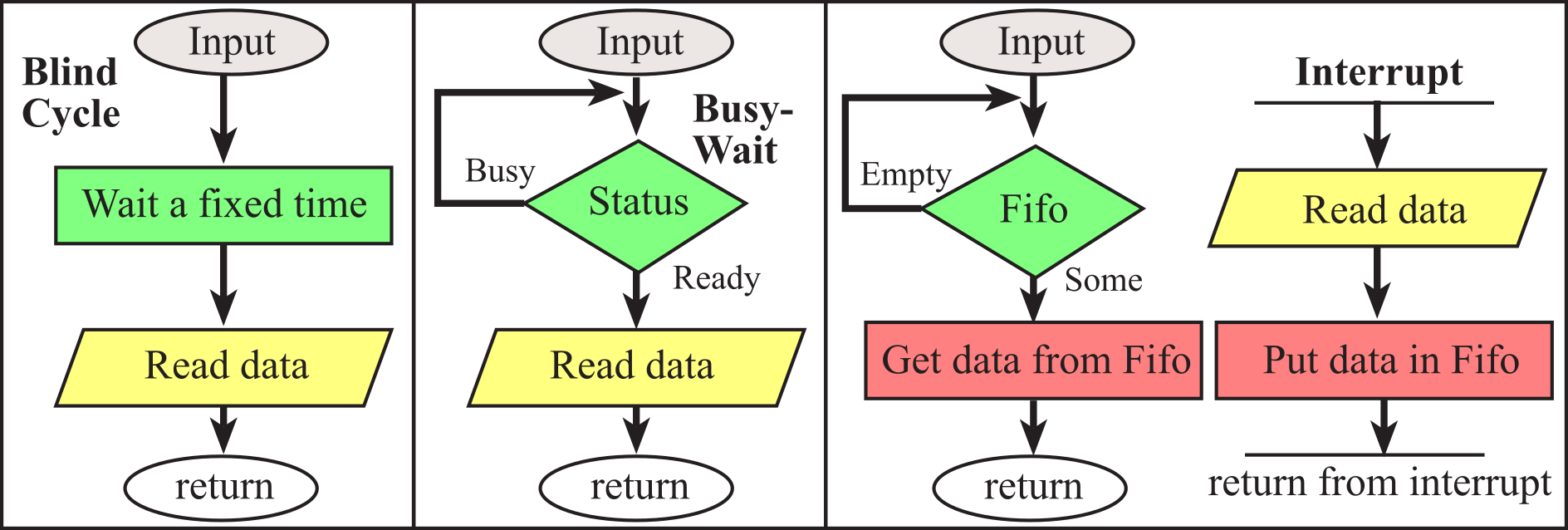
Figure 9.2.1. Synchronization Mechanisms
Video 9.2.1. Device Communication requires Synchronization
Blind cycle is a method where the software simply waits a fixed amount of time and assumes the I/O will complete before that fixed delay has elapsed. For an input device, the software triggers (starts) the external input hardware, waits a specified time, then reads data from device. Blind cycle synchronization for an input device is shown on the left part of Figure 9.2.1. For an output device, shown on the left part of Figure 9.2.2, the software writes data to the output device, triggers (starts) the device, then waits a specified time. We call this method blind, because there is no status information about the I/O device reported to the software. It is appropriate to use this method in situations where the I/O speed is short and predictable. We can ask the LCD to display an ASCII character, wait 37 µs, and then we are sure the operation is complete. This method works because the LCD speed is short and predictable. Another good example of blind-cycle synchronization is spinning a stepper motor. If we repeat this 8-step sequence over and over 1) output a 0x05, 2) wait 1ms, 3) output a 0x06, 4) wait 1ms, 5) output a 0x0A, 6) wait 1ms, 7) output a 0x09, 8) wait 1ms, the motor will spin at a constant speed.
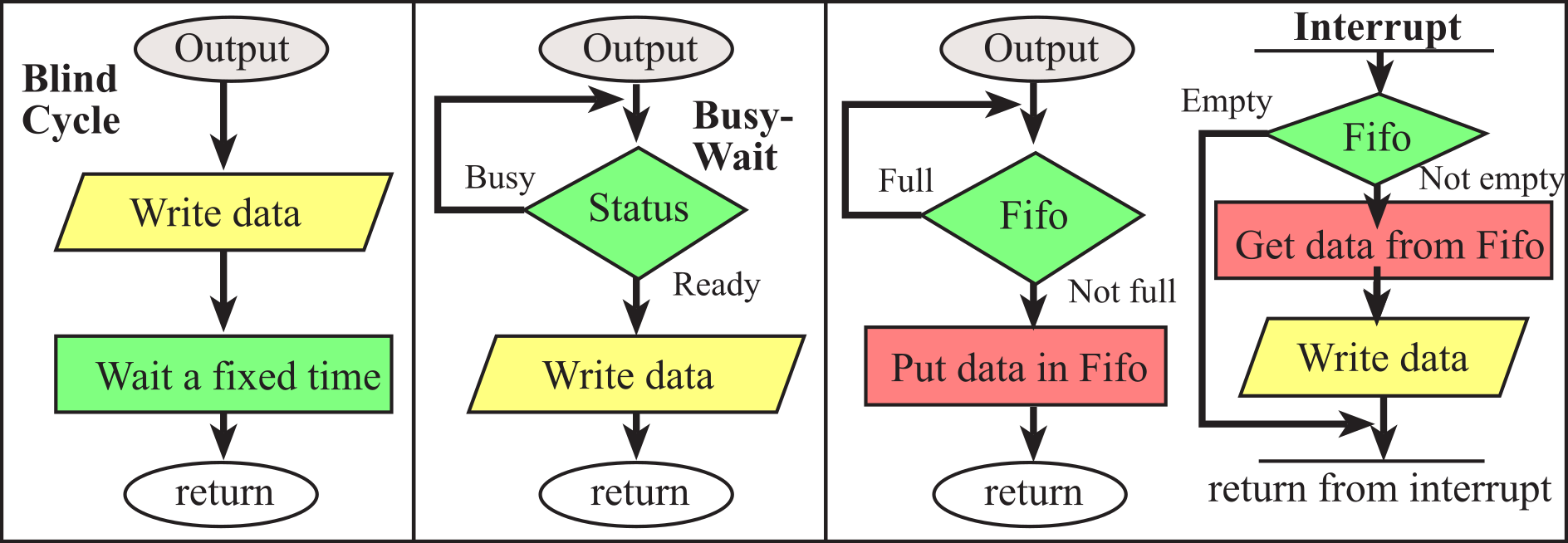
Figure 9.2.2. The output device sets a flag when it has finished outputting the last data.
Use the following tool to see how blind-cycle synchronization works. You will need to enter a number between 1-10 to simulate the timing behavior of the device.
Busy Wait is a software loop that checks the I/O status waiting for the done state. For an input device, the software waits until the input device has new data, and then reads it from the input device, see the middle parts of Figures 9.2.1 and 9.2.2. For an output device, the software writes data, triggers the output device then waits until the device is finished. Another approach to output device interfacing is for the software to wait until the output device has finished the previous output, write data, and then trigger the device. Busy-wait synchronization will be used in situations where the software system is relatively simple and real-time response is not important. The UART software in this chapter will use busy-wait synchronization.
Use the following tool to see how busy-wait synchronization works. You will press the "Ready" button to simulate the device being ready
An interrupt uses hardware to cause special software execution. With an input device, the hardware will request an interrupt when input device has new data. The software interrupt service will read from the input device and save in global RAM, see the right parts of Figures 9.2.1 and 9.2.2. With an output device, the hardware will request an interrupt when the output device is idle. The software interrupt service will get data from a global structure, and then write to the device. Sometimes we configure the hardware timer to request interrupts on a periodic basis. The software interrupt service will perform a special function. A data acquisition system needs to read the ADC at a regular rate. Interrupt synchronization will be used in situations where the system is fairly complex (e.g., a lot of I/O devices) or when real-time response is important.
Use the following tool to see how interrupt-based synchronization works. The foreground thread and background thread (the Interrupt Service Routine or ISR) communicate using a buffer called a first in first out queue (FIFO)
One can think of the hardware being in one of three states. The idle state is when the device is disabled or inactive. No I/O occurs in the idle state. When active (not idle) the hardware toggles between the busy and ready states. The interface includes a flag specifying either busy (0) or ready (1) status. Hardware-software synchronization revolves around this flag:
· The hardware will set the flag when the hardware component is complete.
· The software can read the flag to determine if the device is busy or ready.
· The software can clear the flag, signifying the software component is complete.
· This flag serves as the hardware triggering event for an interrupt.
For an input device, a status flag is set when new input data is available. The “busy to ready” state transition will cause a busy-wait loop to complete, see middle of Figure 9.2.1. Once the software recognizes the input device has new data, it will read the data and ask the input device to create more data. It is the busy to ready state transition that signals to the software that the hardware task is complete, and now software service is required. When the hardware is in the ready state the I/O transaction is complete. Often the simple process of reading the data will clear the flag and request another input.
The problem with I/O devices is that they are usually much slower than software execution. Therefore, we need synchronization, which is the process of the hardware and software waiting for each other in a manner such that data is properly transmitted. A way to visualize this synchronization is to draw a state versus time plot of the activities of the hardware and software. For an input device, the software begins by waiting for new input. When the input device is busy it is in the process of creating new input. When the input device is ready, new data is available. When the input device makes the transition from busy to ready, it releases the software to go forward. In a similar way, when the software accepts the input, it can release the input device hardware. The arrows in Figure 9.2.3 represent the synchronizing events. In this example, the time for the software to read and process the data is less than the time for the input device to create new input. This situation is called I/O bound, meaning the bandwidth is limited by the speed of the I/O hardware.

Figure 9.2.3. The software must wait for the input device to be ready (I/O bound input interface).
If the input device were faster than the software, then the software waiting time would be zero. This situation is called CPU bound (meaning the bandwidth is limited by the speed of the executing software). In real systems the bandwidth depends on both the hardware and the software. Another characteristic of real systems is the data can vary over time, like car traffic arriving and leaving a road intersection. In other words, the same I/O channel can sometimes be I/O bound, but at other times the channel could be CPU bound.
The busy-wait method is classified as unbuffered because the hardware and software must wait for each other during the transmission of each piece of data. The interrupt solution (shown in the right part of Figure 9.2.1) is classified as buffered, because the system allows the input device to run continuously, filling a FIFO with data as fast as it can. In the same way, the software can empty the buffer whenever it is ready and whenever there is data in the buffer. The buffering used in an interrupt interface may be a hardware FIFO, a software FIFO, or both hardware and software FIFOs. We will see the FIFO queues will allow the I/O interface to operate during both situations: I/O bound and CPU bound.
For an output device, a status flag is set when the output is idle and ready to accept more data. The “busy to ready” state transition causes a busy-wait loop to complete, see the middle part of Figure 9.2.2. Once the software recognizes the output is idle, it gives the output device another piece of data to output. It will be important to make sure the software clears the flag each time new output is started. Figure 9.2.4 contains a state versus time plot of the activities of the output device hardware and software. For an output device, the software begins by generating data then sending it to the output device. When the output device is busy it is processing the data. Normally when the software writes data to an output port, that only starts the output process. The time it takes an output device to process data is usually longer than the software execution time. When the output device is done, it is ready for new data. When the output device makes the transition from busy to ready, it releases the software to go forward. In a similar way, when the software writes data to the output, it releases the output device hardware. The output interface illustrated in Figure 9.2.4 is also I/O bound because the time for the output device to process data is longer than the time for the software to generate and write it. Again, I/O bound means the bandwidth is limited by the speed of the I/O hardware.

Figure 9.2.4. The software must wait for the output device to finish the previous operation (I/O bound).
The busy-wait solution for this output interface is also unbuffered, because when the hardware is done, it will wait for the software and after the software generates data, it waits for the hardware. On the other hand, the interrupt solution (shown as the right part of Figure 9.2.2) is buffered, because the system allows the software to run continuously, filling a FIFO as fast as it wishes. In the same way, the hardware can empty the buffer whenever it is ready and whenever there is data in the FIFO. Again, FIFO queues allow the I/O interface to operate during both situations: I/O bound and CPU bound.
On some systems an interrupt will be generated on a hardware failure. Examples include power failure, temperature too high, memory failure, and mechanical tampering of secure systems. Usually, these events are extremely important and require immediate attention. The Cortex™-M processor will execute special software (fault) when it tries to execute an illegal instruction, access an illegal memory location, or attempt an illegal I/O operation.
Video 9.3.1. UART Background and Launchpad Support
In this section we will develop a simple device driver using the Universal Asynchronous Receiver/Transmitter (UART). This serial port allows the microcontroller to communicate with devices such as other computers, printers, input sensors, and LCDs. Serial transmission involves sending one bit at a time, such that the data is spread out over time. The total number of bits transmitted per second is called the baud rate. The reciprocal of the baud rate is the bit time, which is the time to send one bit. Most microcontrollers have at least one UART. The LM4F120/TM4C123 has 8 UARTs. Before discussing the detailed operation on the TM4C, we will begin with general features common to all devices. Each UART will have a baud rate control register, which we use to select the transmission rate. Each device is capable of creating its own serial clock with a transmission frequency approximately equal to the serial clock in the computer with which it is communicating. A frame is the smallest complete unit of serial transmission. Figure 9.3.1 plots the signal versus time on a serial port, showing a single frame, which includes a start bit (which is 0), 8 bits of data (least significant bit first), and a stop bit (which is 1). There is always only one start bit, but the Stellaris® UARTs allow us to select the 5 to 8 data bits and 1 or 2 stop bits. The UART can add even, odd, or no parity bit. However, we will employ the typical protocol of 1 start bit, 8 data bits, no parity, and 1 stop bit. This protocol is used for both transmitting and receiving. The information rate, or bandwidth, is defined as the amount of data or useful information transmitted per second. From Figure 9.3.1, we see that 10 bits are sent for every byte of usual data. Therefore, the bandwidth of the serial channel (in bytes/second) is the baud rate (in bits/sec) divided by 10.

Figure 9.3.1. A serial data frame with 8-bit data, 1 start bit, 1 stop bit, and no parity bit.
Common Error: If you change the bus clock frequency without changing the baud rate register, the UART will operate at an incorrect baud rate.
: Assuming the protocol drawn in Figure 9.3.1 and a baud rate of 1000 bits/sec, what is the bandwidth in bytes/sec?
9.3.1. Asynchronous Communication
We will begin with transmission, because it is simple. The transmitter portion of the UART includes a data output pin, with digital logic levels as drawn in the following interactive tool. The transmitter has a 16-element FIFO and a 10-bit shift register, which cannot be directly accessed by the programmer. The FIFO and shift register in the transmitter are separate from the FIFO and shift register associated with the receiver. In other words each UART has a receiver and a transmitter, but the interactive tool just shows the transmitter on one microcontroller and the receiver on the other. To output data using the UART, the transmitter software will first check to make sure the transmit FIFO is not full (it will wait if TXFF is 1) and then write to the transmit data register (e.g., UART0_DR_R). The bits are shifted out in this order: start, b0, b1, b2, b3, b4, b5, b6, b7, and then stop, where b0 is the LSB and b7 is the MSB. The transmit data register is write only, which means the software can write to it (to start a new transmission) but cannot read from it. Even though the transmit data register is at the same address as the receive data register, the transmit and receive data registers are two separate registers. The transmission software can write to its data register if its TXFF (transmit FIFO full) flag is zero. TXFF equal to zero means the FIFO is not full and has room. The receiving software can read from its data register if its RXFE (receive FIFO empty) flag is zero. RXFE equal to zero means the FIFO is not empty and has some data. While playing the following interactive tool, watch the behavior of the TXFF and RXFE flags.
Use the following tool to watch the steps involved in Serial Communication of a simple two-byte message. Click Start/next over and over to single step the process, and click Run to run the entire sequence.
Click Start to Send 'H' to the direction registerWhen a new byte is written to UART0_DR_R, it is put into the transmit FIFO. Byte by byte, the UART gets data from the FIFO and loads them into the 10-bit transmit shift register. The 10-bit shift register includes a start bit, 8 data bits, and 1 stop bit. Then, the frame is shifted out one bit at a time at a rate specified by the baud rate register. If there are already data in the FIFO or in the shift register when the UART0_DR_R is written, the new frame will wait until the previous frames have been transmitted, before it too is transmitted. The FIFO guarantees the data are transmitted in the order they were written. The serial port hardware is actually controlled by a clock that is 16 times faster than the baud rate, referred to in the datasheet as Baud16. When the data are being shifted out, the digital hardware in the UART counts 16 times in between changes to the U0Tx output line.
The software can actually write 16 bytes to the UART0_DR_R, and the hardware will send them all one at a time in the proper order. This FIFO reduces the software response time requirements of the operating system to service the serial port hardware. Unfortunately, it does complicate the hardware/software timing. At 9600 bits/sec, it takes 1.04 ms to send a frame. Therefore, there will be a delay ranging from 1.04 and 16.7 ms between writing to the data register and the completion of the data transmission. This delay depends on how much data are already in the FIFO at the time the software writes to UART0_DR_R.
Receiving data frames is a little trickier than transmission because we have to synchronize the receive shift register with the incoming data. The receiver portion of the UART includes a U0Rx data input pin with digital logic levels. At the input of the microcontroller, true is 3.3V and false is 0V. There is also a 16-element FIFO and a 10-bit shift register, which cannot be directly accessed by the programmer (shown on the right side of the interactive tool). The receive shift register is 10 bits wide, but the FIFO is 12 bits, 8 bits of data and 4 error flags. Again the receive shift register and receive FIFO are separate from those in the transmitter. The receive data register, UART0_DR_R, is read only, which means write operations to this address have no effect on this register (recall write operations activate the transmitter). The receiver obviously cannot start a transmission, but it recognizes a new frame by its start bit. The bits are shifted in using the same order as the transmitter shifted them out: start, b0, b1, b2, b3, b4, b5, b6, b7, and then stop.
There are six status bits generated by receiver activity. The Receive FIFO empty flag, RXFE, is clear when new input data are in the receive FIFO. When the software reads from UART0_DR_R, data are removed from the FIFO. When the FIFO becomes empty, the RXFE flag will be set, meaning there are no more input data. There are other flags associated with the receiver. There is a Receive FIFO full flag RXFF, which is set when the FIFO is full. There are four status bits associated with each byte of data. For this reason, the receive FIFO is 12 bits wide. The overrun error, OE, is set when input data are lost because the FIFO is full and more input frames are arriving at the receiver. An overrun error is caused when the receiver interface latency is too large. The break error, BE, is set when the input is held low for more than a frame. Parity is a mechanism to send one extra bit so the receiver can detect if there were any errors in transmission. With even parity the number of 1's in the data plus parity will be an even number. The PE bit is set on a parity error. Because the error rate is so low, most systems do not implement parity. We will not use parity in this class. The framing error, FE, is set when the stop bit is incorrect. Framing errors are probably caused by a mismatch in baud rate.
The receiver waits for the 1 to 0 edge signifying a start bit, then shifts in 10 bits of data one at a time from the U0Rx line. The internal clock is 16 times faster than the baud rate. After the 1 to 0 edge, the receiver waits 8 internal clocks and samples the start bit. 16 internal clocks later it samples b0. Every 16 internal clocks it samples another bit until it reaches the stop bit. The UART needs an internal clock faster than the baud rate so it can wait the half a bit time between the 1 to 0 edge beginning the start bit and the middle of the bit window needed for sampling. The start and stop bits are removed (checked for framing errors), the 8 bits of data and 4 bits of status are put into the receive FIFO. The hardware FIFO implements buffering so data is safely stored in the receiver hardware if the software is performing other tasks while data is arriving.
Observation: If the receiving UART device has a baud rate mismatch of more than 5%, then a framing error can occur when the stop bit is incorrectly captured.
An overrun occurs when there are 16 elements in the receive FIFO, and a 17th frame comes into the receiver. In order to avoid overrun, we can design a real-time system, i.e., one with a maximum latency. The latency of a UART receiver is the delay between the time when new data arrives in the receiver (RXFE=0) and the time the software reads the data register. If the latency is always less than 160 bit times, then overrun will never occur.
Observation: With a serial port that has a shift register and one data register (no FIFO buffering), the latency requirement of the input interface is the time it takes to transmit one data frame.
9.3.2. TM4C UART Details
Next we will overview the specific UART functions on the TM4C microcontroller. This section is intended to supplement rather than replace the Texas Instruments manuals. When designing systems with any I/O module, you must also refer to the reference manual of your specific microcontroller. It is also good design practice to review the errata for your microcontroller to see if any quirks (mistakes) exist in your microcontroller that might apply to the system you are designing.
Stellaris TM4C microcontrollers have eight UARTs. The specific port pins used to implement the UARTs vary from one chip to the next. To find which pins your microcontroller uses, you will need to consult its datasheet. Table 9.2 shows some of the registers for the UART0 and UART1. For the other UARTs, the register names will replace the 0 with a 1 – 7. For the exact register addresses, you should include the appropriate header file (e.g., tm4c123gh6pm.h). To activate a UART you will need to turn on the UART clock in the RCGCUART register. You should also turn on the clock for the digital port in the RCGCGPIO register. You need to enable the transmit and receive pins as digital signals. The alternative function for these pins must also be selected. In particular we set bits in both the AFSEL and PCTL registers.
The OE, BE, PE, and FE are error flags associated with the receiver. You can see these flags in two places: associated with each data byte in UART0_DR_R or as a separate error register in UART0_RSR_R. The overrun error (OE) is set if data has been lost because the input driver latency is too long. BE is a break error, meaning the other device has sent a break. PE is a parity error (however, we will not be using parity). The framing error (FE) will get set if the baud rates do not match. The software can clear these four error flags by writing any value to UART0_RSR_R.
The status of the two FIFOs can be seen in the UART0_FR_R register. The BUSY flag is set while the transmitter still has unsent bits, even if the transmitter is disabled. It will become zero when the transmit FIFO is empty and the last stop bit has been sent. If you implement busy-wait output by first outputting then waiting for BUSY to become 0 (right flowchart of Figure 9.10), then the routine will write new data and return after that particular data has been completely transmitted.
The UART0_CTL_R control register contains the bits that turn on the UART. TXE is the Transmitter Enable bit, and RXE is the Receiver Enable bit. We set TXE, RXE, and UARTEN equal to 1 in order to activate the UART device. However, we should clear UARTEN during the initialization sequence.
|
|
31–12 |
11 |
10 |
9 |
8 |
7–0 |
Name |
||
|
$4000.C000 |
|
OE |
BE |
PE |
FE |
DATA |
UART0_DR_R |
||
|
|
|
|
|
|
|
|
|
|
|
|
|
31–3 |
3 |
2 |
1 |
0 |
|
|||
|
$4000.C004 |
|
OE |
BE |
PE |
FE |
UART0_RSR_R |
|||
|
|
|
|
|
|
|
|
|
|
|
|
|
31–8 |
7 |
6 |
5 |
4 |
3 |
2–0 |
|
|
|
$4000.C018 |
|
TXFE |
RXFF |
TXFF |
RXFE |
BUSY |
|
UART0_FR_R |
|
|
|
|
|
|
|
|
|
|
|
|
|
|
31–16 |
15–0 |
|
||||||
|
$4000.C024 |
|
DIVINT |
UART0_IBRD_R |
||||||
|
|
|
|
|
|
|
|
|
|
|
|
|
31–6 |
5–0 |
|
||||||
|
$4000.C028 |
|
DIVFRAC |
UART0_FBRD_R |
||||||
|
|
|
|
|
|
|
|
|
|
|
|
|
|
7 |
6 – 5 |
4 |
3 |
2 |
1 |
0 |
|
|
$4000.C02C |
|
SPS |
WPEN |
FEN |
STP2 |
EPS |
PEN |
BRK |
UART0_LCRH_R |
|
|
|
|
|
|
|
|
|
|
|
|
|
31–10 |
9 |
8 |
7 |
6–3 |
2 |
1 |
0 |
|
|
$4000.C030 |
|
RXE |
TXE |
LBE |
|
SIRLP |
SIREN |
UARTEN |
UART0_CTL_R |
|
|
|
|
|
|
|
|
|
||
|
|
31–12 |
11 |
10 |
9 |
8 |
7–0 |
|
||
|
$4000.D000 |
|
OE |
BE |
PE |
FE |
DATA |
UART1_DR_R |
||
|
|
|
|
|
|
|
|
|
|
|
|
|
31–3 |
3 |
2 |
1 |
0 |
|
|||
|
$4000.D004 |
|
OE |
BE |
PE |
FE |
UART1_RSR_R |
|||
|
|
|
|
|
|
|
|
|
|
|
|
|
31–8 |
7 |
6 |
5 |
4 |
3 |
2–0 |
|
|
|
$4000.D018 |
|
TXFE |
RXFF |
TXFF |
RXFE |
BUSY |
|
UART1_FR_R |
|
|
|
|
|
|
|
|
|
|
|
|
|
|
31–16 |
15–0 |
|
||||||
|
$4000.D024 |
|
DIVINT |
UART1_IBRD_R |
||||||
|
|
|
|
|
|
|
|
|
|
|
|
|
31–6 |
5–0 |
|
||||||
|
$4000.D028 |
|
DIVFRAC |
UART1_FBRD_R |
||||||
|
|
|
|
|
|
|
|
|
|
|
|
|
31–8 |
7 |
6 – 5 |
4 |
3 |
2 |
1 |
0 |
|
|
$4000.D02C |
|
SPS |
WPEN |
FEN |
STP2 |
EPS |
PEN |
BRK |
UART1_LCRH_R |
|
|
|
|
|
|
|
|
|
|
|
|
|
31–10 |
9 |
8 |
7 |
6–3 |
2 |
1 |
0 |
|
|
$4000.D030 |
|
RXE |
TXE |
LBE |
|
SIRLP |
SIREN |
UARTEN |
UART1_CTL_R |
Table 9.2. Some UART registers. Each register is 32 bits wide. Shaded bits are zero.
The IBRD and FBRD registers specify the baud rate. The baud rate divider is a 22-bit binary fixed-point value with a resolution of 2-6. The Baud16 clock is created from the system bus clock, with a frequency of (Bus clock frequency)/divider. The baud rate is 16 times slower than Baud16
Baud rate = Baud16/16 = (Bus clock frequency)/(16*divider)
For example, if the bus clock is 80 MHz and the desired baud rate is 19200 bits/sec, then the divider should be 80,000,000/16/19200 or 260.4167. Let m be the integer part, without rounding. We store the integer part (m=260) in IBRD. For the fraction, we find an integer n, such that n/64 is about 0.4167. More simply, we multiply 0.4167*64 = 26.6688 and round to the closest integer, 27. We store this fraction part (n=27) in FBRD. We did approximate the divider, so it is interesting to determine the actual baud rate. Assume the bus clock is 80 MHz.
Baud rate = (80 MHz)/(16* (m+n/64)) = (80 MHz)/(16* (260+27/64)) = 19199.616 bits/sec
The baud rates in the transmitter and receiver must match within 5% for the channel to operate properly. The error for this example is 0.002%.
The three registers LCRH, IBRD, and FBRD form an internal 30-bit register. This internal register is only updated when a write operation to LCRH is performed, so any changes to the baud-rate divisor must be followed by a write to the LCRH register for the changes to take effect. Out of reset, both FIFOs are disabled and act as 1-byte-deep holding registers. The FIFOs are enabled by setting the FEN bit in LCRH.
: Assume the bus clock is 10 MHz. What is the baud rate if UART0_IBRD_R equals 2 and UART0_FBRD_R equals 32?
: Assume the bus clock is 50 MHz. What values should you put in UART0_IBRD_R and UART0_FBRD_R to make a baud rate of 38400 bits/sec?
9.3.3. UART1 Device Driver on PC5 and PC4
Software that sends and receives data must implement a mechanism to synchronize the software with the hardware. In particular, the software should read data from the input device only when data is indeed ready. Similarly, software should write data to an output device only when the device is ready to accept new data. With busy-wait synchronization, the software continuously checks the hardware status waiting for it to be ready. In this section, we will use busy-wait synchronization to write I/O programs that send and receive data using the UART. After a frame is received, the receive FIFO will be not empty (RXFE becomes 0) and the 8-bit data is available to be read. To get new data from the serial port, the software first waits for RXFE to be zero, then reads the result from UART1_DR_R. Recall that when the software reads UART1_DR_R it gets data from the receive FIFO. This operation is illustrated in Figure 9.3.2 and shown in Program 9.1. In a similar fashion, when the software wishes to output via the serial port, it first waits for TXFF to be clear, then performs the output. When the software writes UART1_DR_R it puts data into the transmit FIFO.
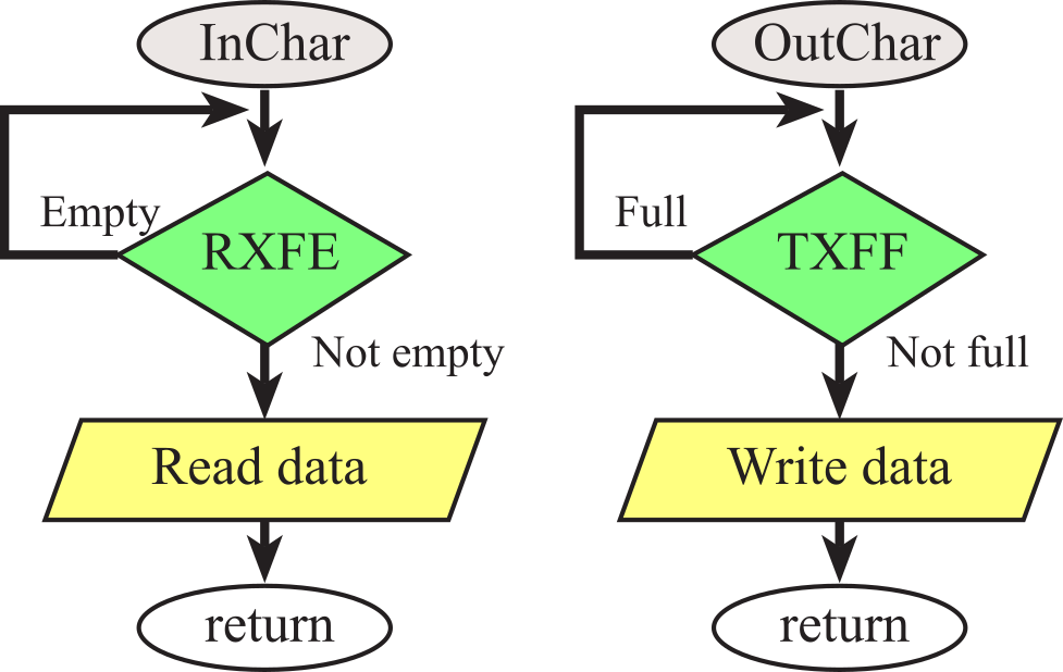
Figure 9.3.2. Flowcharts of InChar and OutChar using busy-wait synchronization.
The initialization program, UART_Init, enables the UART1 device and selects the baud rate. The PCTL bits were defined back in Chapter 6, and repeated as Table 9.3. PCTL bits 5-4 are set to 0x22 to select U1Tx and U1Rx on PC5 and PC4. The input routine waits in a loop until RXFE is 0 (FIFO not empty), then reads the data register. The output routine first waits in a loop until TXFF is 0 (FIFO not full), then writes data to the data register. Polling before writing data is an efficient way to perform output. UART2_xxx.zip is the interrupt-driven version. Be careful when using Port C to be friendly; the pins PC3-PC0 are used by the debugger and you should not modify their configurations.
|
IO |
Ain |
0 |
1 |
2 |
3 |
4 |
5 |
6 |
7 |
8 |
9 |
14 |
|
PA0 |
|
Port |
U0Rx |
|
|
|
|
|
|
CAN1Rx |
|
|
|
PA1 |
|
Port |
U0Tx |
|
|
|
|
|
|
CAN1Tx |
|
|
|
PA2 |
|
Port |
|
SSI0Clk |
|
|
|
|
|
|
|
|
|
PA3 |
|
Port |
|
SSI0Fss |
|
|
|
|
|
|
|
|
|
PA4 |
|
Port |
|
SSI0Rx |
|
|
|
|
|
|
|
|
|
PA5 |
|
Port |
|
SSI0Tx |
|
|
|
|
|
|
|
|
|
PA6 |
|
Port |
|
|
I2C1SCL |
|
M1PWM2 |
|
|
|
|
|
|
PA7 |
|
Port |
|
|
I2C1SDA |
|
M1PWM3 |
|
|
|
|
|
|
PB0 |
|
Port |
U1Rx |
|
|
|
|
|
T2CCP0 |
|
|
|
|
PB1 |
|
Port |
U1Tx |
|
|
|
|
|
T2CCP1 |
|
|
|
|
PB2 |
|
Port |
|
|
I2C0SCL |
|
|
|
T3CCP0 |
|
|
|
|
PB3 |
|
Port |
|
|
I2C0SDA |
|
|
|
T3CCP1 |
|
|
|
|
PB4 |
Ain10 |
Port |
|
SSI2Clk |
|
M0PWM2 |
|
|
T1CCP0 |
CAN0Rx |
|
|
|
PB5 |
Ain11 |
Port |
|
SSI2Fss |
|
M0PWM3 |
|
|
T1CCP1 |
CAN0Tx |
|
|
|
PB6 |
|
Port |
|
SSI2Rx |
|
M0PWM0 |
|
|
T0CCP0 |
|
|
|
|
PB7 |
|
Port |
|
SSI2Tx |
|
M0PWM1 |
|
|
T0CCP1 |
|
|
|
|
PC4 |
C1- |
Port |
U4Rx |
U1Rx |
|
M0PWM6 |
|
IDX1 |
WT0CCP0 |
U1RTS |
|
|
|
PC5 |
C1+ |
Port |
U4Tx |
U1Tx |
|
M0PWM7 |
|
PhA1 |
WT0CCP1 |
U1CTS |
|
|
|
PC6 |
C0+ |
Port |
U3Rx |
|
|
|
|
PhB1 |
WT1CCP0 |
USB0epen |
|
|
|
PC7 |
C0- |
Port |
U3Tx |
|
|
|
|
|
WT1CCP1 |
USB0pflt |
|
|
|
PD0 |
Ain7 |
Port |
SSI3Clk |
SSI1Clk |
I2C3SCL |
M0PWM6 |
M1PWM0 |
|
WT2CCP0 |
|
|
|
|
PD1 |
Ain6 |
Port |
SSI3Fss |
SSI1Fss |
I2C3SDA |
M0PWM7 |
M1PWM1 |
|
WT2CCP1 |
|
|
|
|
PD2 |
Ain5 |
Port |
SSI3Rx |
SSI1Rx |
|
M0Fault0 |
|
|
WT3CCP0 |
USB0epen |
|
|
|
PD3 |
Ain4 |
Port |
SSI3Tx |
SSI1Tx |
|
|
|
IDX0 |
WT3CCP1 |
USB0pflt |
|
|
|
PD4 |
USB0DM |
Port |
U6Rx |
|
|
|
|
|
WT4CCP0 |
|
|
|
|
PD5 |
USB0DP |
Port |
U6Tx |
|
|
|
|
|
WT4CCP1 |
|
|
|
|
PD6 |
|
Port |
U2Rx |
|
|
M0Fault0 |
|
PhA0 |
WT5CCP0 |
|
|
|
|
PD7 |
|
Port |
U2Tx |
|
|
|
|
PhB0 |
WT5CCP1 |
NMI |
|
|
|
PE0 |
Ain3 |
Port |
U7Rx |
|
|
|
|
|
|
|
|
|
|
PE1 |
Ain2 |
Port |
U7Tx |
|
|
|
|
|
|
|
|
|
|
PE2 |
Ain1 |
Port |
|
|
|
|
|
|
|
|
|
|
|
PE3 |
Ain0 |
Port |
|
|
|
|
|
|
|
|
|
|
|
PE4 |
Ain9 |
Port |
U5Rx |
|
I2C2SCL |
M0PWM4 |
M1PWM2 |
|
|
CAN0Rx |
|
|
|
PE5 |
Ain8 |
Port |
U5Tx |
|
I2C2SDA |
M0PWM5 |
M1PWM3 |
|
|
CAN0Tx |
|
|
|
PF0 |
|
Port |
U1RTS |
SSI1Rx |
CAN0Rx |
|
M1PWM4 |
PhA0 |
T0CCP0 |
NMI |
C0o |
|
|
PF1 |
|
Port |
U1CTS |
SSI1Tx |
|
|
M1PWM5 |
PhB0 |
T0CCP1 |
|
C1o |
TRD1 |
|
PF2 |
|
Port |
|
SSI1Clk |
|
M0Fault0 |
M1PWM6 |
|
T1CCP0 |
|
|
TRD0 |
|
PF3 |
|
Port |
|
SSI1Fss |
CAN0Tx |
|
M1PWM7 |
|
T1CCP1 |
|
|
TRCLK |
|
PF4 |
|
Port |
|
|
|
|
M1Fault0 |
IDX0 |
T2CCP0 |
USB0epen |
|
|
Table 9.3. PMCx bits in the GPIOPCTL register on the LM4F/TM4C specify alternate functions. PD4 and PD5 are hardwired to the USB device. PA0 and PA1 are hardwired to the serial port.
// Assumes a 80 MHz bus clock, creates 115200 baud rate
void UART_Init(void){ // should be called only once
SYSCTL_RCGCUART_R |= 0x00000002; // activate UART1
SYSCTL_RCGCGPIO_R |= 0x00000004; // activate port C
UART1_CTL_R &= ~0x00000001; // disable UART
UART1_IBRD_R = 43; // IBRD = int(80,000,000/(16*115,200)) = int(43.40278)
UART1_FBRD_R = 26; // FBRD = round(0.40278 * 64) = 26
UART1_LCRH_R = 0x00000070; // 8 bit, no parity bits, one stop, FIFOs
UART1_CTL_R |= 0x00000001; // enable UART
GPIO_PORTC_AFSEL_R |= 0x30; // enable alt funct on PC5-4
GPIO_PORTC_DEN_R |= 0x30; // configure PC5-4 as UART1
GPIO_PORTC_PCTL_R = (GPIO_PORTC_PCTL_R&0xFF00FFFF)+0x00220000;
GPIO_PORTC_AMSEL_R &= ~0x30; // disable analog on PC5-4
}
// Wait for new input, then return ASCII code
char UART_InChar(void){
while((UART1_FR_R&0x0010) != 0); // wait until RXFE is 0
return((char)(UART1_DR_R&0xFF));
}
// Wait for buffer to be not full, then output
void UART_OutChar(char data){
while((UART1_FR_R&0x0020) != 0); // wait until TXFF is 0
UART1_DR_R = data;
}
// Immediately return input or 0 if no input
char UART_InCharNonBlocking(void){
if((UART1_FR_R&UART_FR_RXFE) == 0){
return((char)(UART1_DR_R&0xFF));
} else{
return 0;
}
}
Program 9.1. Device driver functions that implement serial I/O.
Video 9.3.3. UART Device Driver walk through
: How does the software clear RXFE?
: How does the software clear TXFF?
: Describe what happens if the receiving computer is operating on a baud rate that is twice as fast as the transmitting computer?
: Describe what happens if the transmitting computer is operating on a baud rate that is twice as fast as the receiving computer?
: How do you change Program 9.1 to run at the same baud rate, but the system clock is now 10 MHz.
9.4.1. FIFO Theory
The first in first out circular queue (FIFO) is quite useful for implementing a buffered I/O interface. It can be used for both buffered input and buffered output. The order preserving data structure temporarily saves data created by the source (producer) before it is processed by the sink (consumer). After initialization, the FIFO has two functions: FIFO_Put (enters new data) and FIFO_Get (removes the oldest data). You have probably already experienced the convenience of FIFOs. For example, when using an editor, you can continue to type characters while other processing is occurring. The ASCII codes are input from the keyboard as they are typed and put in a FIFO. When the editor is active again, it gets more keyboard data to process. A FIFO is also used when you ask the computer to print a file. Rather than waiting for the actual printing to occur character by character, the print command will put the data in a FIFO. Whenever the printer is free, it will get data from the FIFO. The advantage of the FIFO is it allows you to continue to use your computer while the printing occurs in the background. To implement this magic of background printing we will need interrupts.

Figure 9.4.1. A data flow graph showing a FIFO that buffers data between a producer and a consumer.
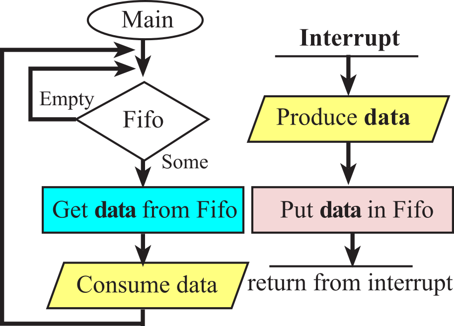
Figure 9.4.2. A flow chart showing a FIFO that buffers data between a producer and a consumer.
We use the FIFO to pass data from the producer to the consumer, as illustrated by Figures 9.4.1 and 9.4.2. In general, the rates at which data are produced and consumed can vary dynamically. Humans do not enter data into a keyboard at a constant rate. Even printers require more time to print color graphics versus black and white text. Let N be the average number of data packets in the queue plus the one data packet currently being processed by the consumer. Basically, N is the average number of packets in the system. Let λ be the average arrival rate in packets per second (pps). Let R be the average response time of a packet, which includes the time waiting in the queue plus the time for the consumer to process the packet. Little’s Theorem states
N = λR
As long as the system is stable, this result is not influenced by the probability distribution of the producer, the probability distribution of the consumer or the service order. Let S be the mean service time for a packet. Thus, C=1/S is defined as the system capacity (pps). Stable in this context means the packet arrival rate is less than the system capacity (λ<C). This means, in most cases, the queue length can be chosen so the queue never fills, and no data are lost. In this case, the arrival rate λ is also the output rate T, or throughput of the system. We can use Little’s Theorem to estimate average response time,
R = N/T
9.4.2. FIFO Implementation
There are many ways to implement a statically allocated FIFO. We can use either a pointer or and index to access the data in the FIFO. We can use either two pointers (or two indices) or two pointers (or two indices) and a counter. The counter specifies how many entries are currently stored in the FIFO. There are even hardware implementations of FIFO queues. If we were to have infinite memory, as shown in Figure 9.4.3, a FIFO implementation is easy. GetI is the index specifying data that will be removed by the next call to Fifo_Get, and PutI is the index to the empty space where the data will be stored by the next call to Fifo_Put. To put data in the FIFO, the new data is stored at PutI, and then this index is incremented. To get data from the FIFO, the value at GetI is read, and then this index is incremented.
void Fifo_Put(int32_t data){
FIFO[PutI] = data;
PutI++;
}
void Fifo_Get(int32_t *datapt){
*datapt = FIFO[GetI];
GetI++;
}
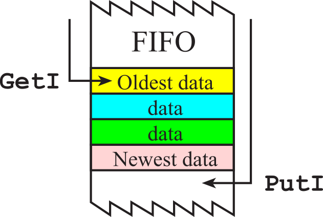
Figure 9.4.3. The FIFO implementation with infinite memory.
There are three modifications that are required to these functions. If the FIFO is full when Fifo_Put is called then the subroutine should return a full error. Similarly, if the FIFO is empty when Fifo_Get is called, then the subroutine should return an empty error. There is never an infinite amount of memory, so a finite number of bytes will be permanently allocated to the FIFO. Figures 9.4.4 and 9.4.5 show an example with 10 words allocated. The PutI and GetI must be wrapped back up to the top when they reach the bottom. The colored blocks in these two figures represent valid data saved in the FIFO. Figure 9.5.10 shows how the FIFO changes as four words are Put into it.
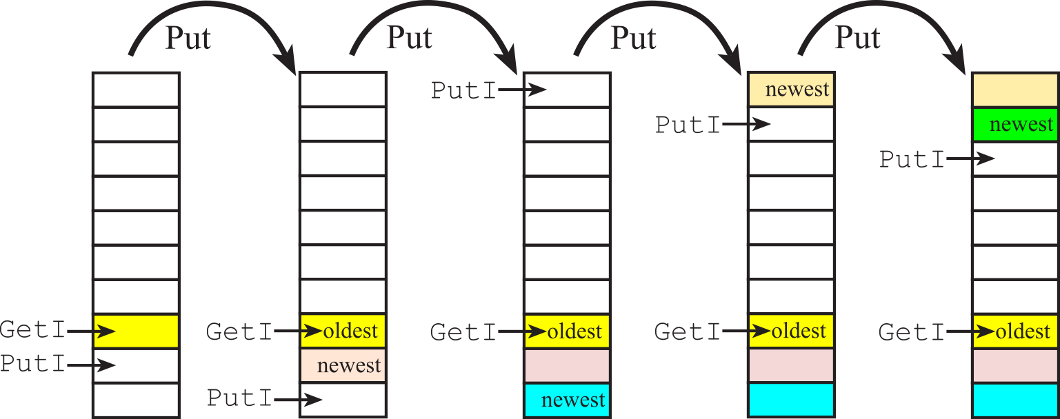
Figure 9.4.4. The FIFO Put operation showing the index wrap.
Figure 9.4.5 shows the same FIFO as Fifo_Get is called four times. Observe the order-preserving nature of the FIFO. Notice also, the data does not move; rather, the indices are changed as data are put and get.
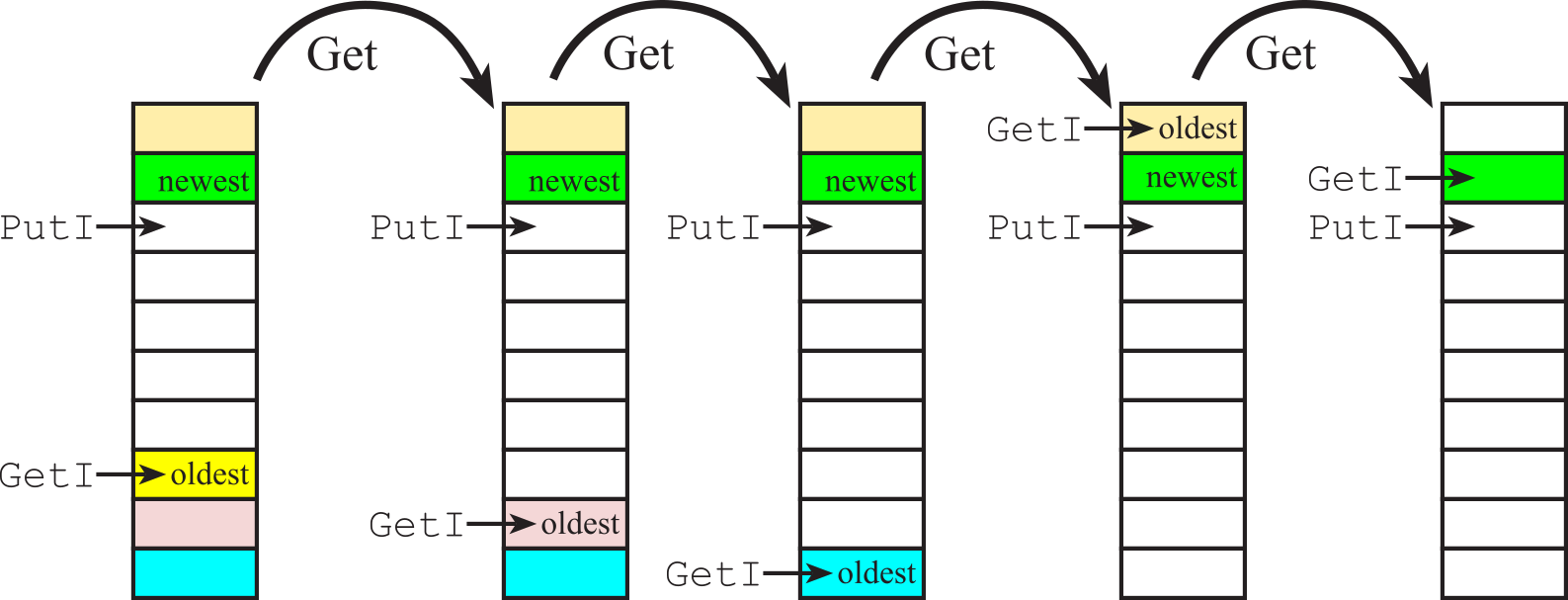
Figure 9.4.5. The FIFO Get operation showing the index wrap.
Video 9.4.1. First in first out queue
There are two mechanisms to determine whether the FIFO is empty or full. A simple method is to implement a counter containing the number of elements currently stored in the FIFO. Fifo_Get would decrement the counter and Fifo_Put would increment the counter. The second method, shown in Figure 9.4.6, is to prevent the FIFO from being completely full. For example, if the FIFO had 7 words allocated, then the Fifo_Put subroutine would allow a maximum of 6 words to be stored. If there were already 6 words in the FIFO and another Fifo_Put were called, then the FIFO would not be modified and a full error would be returned. In this way if PutI equals GetI at the beginning of Fifo_Get, then the FIFO is empty. Similarly, if PutI+1 equals GetI at the beginning of Fifo_Put, then the FIFO is full. Be careful to wrap the PutI+1 before comparing it to GetI. This second method does not require the length to be stored or calculated. The FIFO global structures must be allocated in RAM. PutI and GetI are private, and not accessible by programs outside the FIFO module
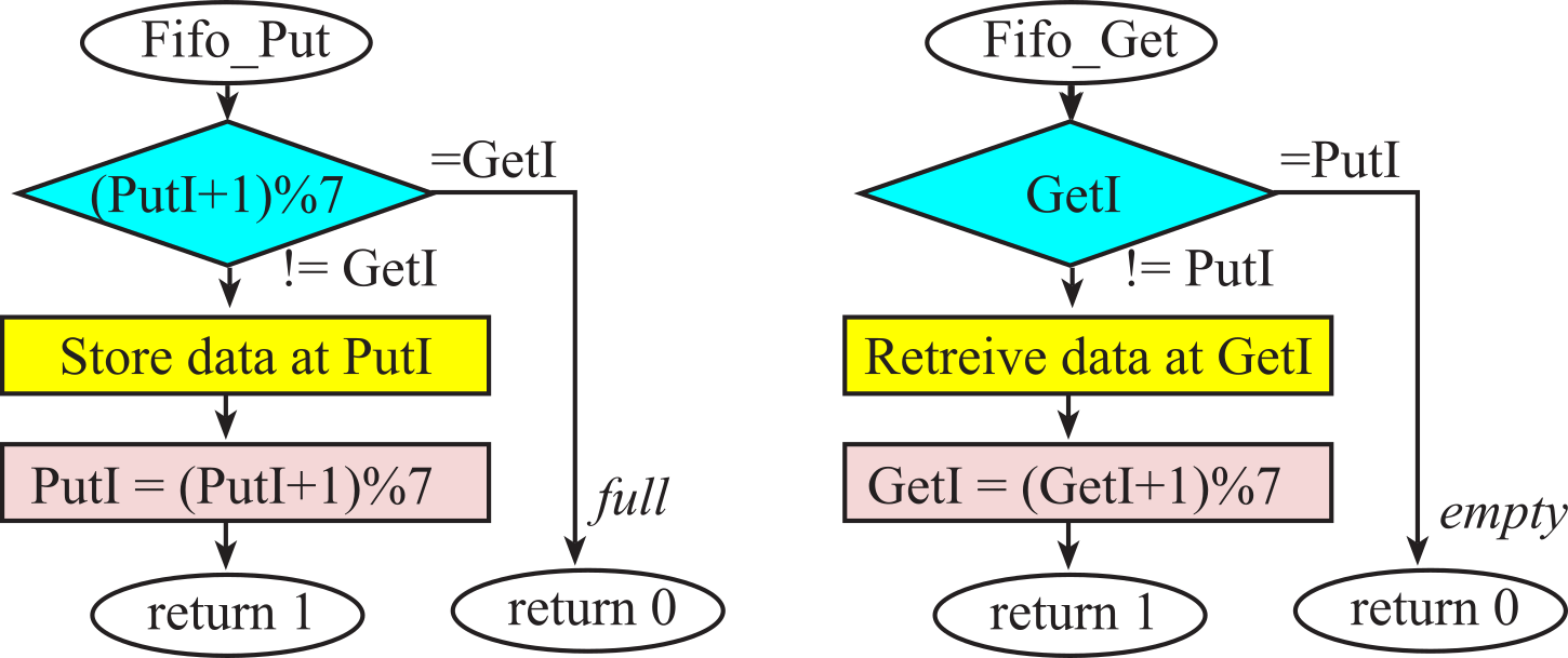
Figure 9.4.6. Flowcharts of the put and get operations.
#define FIFO_SIZE 7
static uint8_t PutI; // index to put new
static uint8_t GetI; // index of oldest
static char Fifo[FIFO_SIZE];
void Fifo_Init(){
PutI = GetI = 0; // empty
}
uint8_t Fifo_Put(char data){
if(((PutI+1)%FIFO_SIZE) == GetI) return 0; // fail if
full
Fifo[PutI] =
data; // save
in Fifo
PutI = (PutI+1)%FIFO_SIZE; // next place to put
return 1;
}
uint8_t Fifo_Get(char *datapt){
if(GetI == PutI) return 0; // fail if empty
*datapt =
Fifo[GetI]; // retrieve data
GetI = (GetI+1)%FIFO_SIZE; // next place to get
return 1;
}
Program 9.2. Implementation of a two-index FIFO
The next video shows you how to implement the FIFO in C++
Video 9.4.2. First in first out queue in C++
: How do we make GetI and PutI permanently allocated but private in scope to the file?
: What bug occurs if we were to add a counter, which is incremented in Fifo_Put and decremented in Fifo_Get?
: Assume a FIFO is initially empty. Next, we Put 1,2,3,4,5 into the FIFO. What value is returned if we call Get?
: Assume a stack is initially empty. Next, we Push 1,2,3,4,5 onto the stack. What value is returned if we call Pop?
9.4.3. FIFO Example Application
In the following video, there is a data acquisition system where data are produced at 1000 samples per second, or one point per ms. Since the data acquisition is interrupt driven, the instantaneous and the average producer rate is exactly 1000 samples/sec. With software averaging, 100 data points are averaged, and every 100ms the average is displayed on the LCD screen. The time to display the average is 6 ms, so it takes 6 ms to consume 100 samples. The average consumer rate is 100/6ms, or 16667 samples/sec. Every 100th point it takes 6ms, and the other 99 points are on the order of about 10us. Therefore, the instantaneous consumer rate varies from a low of 1/6ms(17 samples/sec) to a high of 1/10us (100,000 samples/sec). Since the average producer rate is less than the average consumer rate, the system has a solution. However, a FIFO is needed to prevent data loss during the 6ms it takes to do the LCD output. The next video shows how a FIFO can be used to prevent data loss in this typical application.
Video 9.4.3. Using a First in first out queue in a data acquisition system
void SysTick_Handler(void){ // 1000 Hz sampling, interrupt every 1
ms
uint16_t data = ADC_In(); // new data
Fifo_Put(data); // save data
}
int main(void){uint32_t sum=0,n=0,p;
uint16_t d;
Init(); // other
initialization
Fifo_Init();// this fifo passes 16-bit data
while(1){
while(Fifo_Get(&d)==0){};
sum = sum+d; // average
n = n+1;
if(n == 100){// output every 100th sample
p = Convert(sum/100);
LCD_OutFix(p);
sum = n = 0;
}
}
}
Program 9.3. Using a First in first out queue in a data acquisition system
For details of the UART registers see the appendix section: 6. TM4C123 Universal Asynchronous Receiver Transmitter. There are three fundamental aspects of serial communication common to all UARTs.
- Baud rate
- Format
- Hardware-software synchronization
Baud rate is the number of bits/sec. The baud rate is programmed into both the transmitter and receiver, and the rates should match within 5%. On the TM4C123, see the UART0_IBRD_R and UART0_FBRD_R registers.
The format defines the structure of the serial frame. There is always one start bit, but the number of data bits can vary. Most UARTs can add no, even, or odd parity. Many UARTs can operate with 1 or 2 stop bits. Just like baud rate, the format is programmed into both the transmitter and receiver, and the formats must match. On the TM4C123, see the the UART0_LCRH_R register.
We could use busy-wait or interrupt synchrononization. Different from baud rate and format, the tranmitter and receiver do not need to use the same synchronization. For efficient performance, we will use busy-wait only when we know the software will never wait. For example, if the size of the tranmitted message is less than the size of the hardware TxFifo, and the rate of sending message allows the previous message to be completely sent before the next message is attempted, then busy-wait in the transmitter is allowed because it will never wait. Often this timing cannot be guaranteed, so interrupts are needed. To use interrupts we will enable the FIFOs by setting the FEN bit in the UART0_LCRH_R register. RXIFLSEL specifies the receive FIFO level that causes an interrupt.
RXIFLSEL
Set RXRIS interrupt trigger when
0x0 ≥ 1/8 full Receive FIFO goes from 1
to 2 characters
0x1 ≥ 1/4 full Receive FIFO goes from 3
to 4 characters
0x2 ≥ 1/2 full Receive FIFO goes from 7 to 8
characters
0x3 ≥ 3/4 full Receive FIFO goes from 11
to 12 characters
0x4 ≥ 7/8 full Receive FIFO goes from 13
to 14 characters
TXIFLSEL specifies the transmit FIFO level that causes an
interrupt.
TXIFLSEL
Set TXRIS
interrupt trigger when
0x0 ≤ 7/8 empty Transmit FIFO goes from 15 to 14
characters
0x1 ≤ 3/4 empty Transmit FIFO goes from 13 to 12
characters
0x2 ≤ 1/2 empty Transmit FIFO goes from 9 to 8
characters
0x3 ≤ 1/4 empty Transmit FIFO goes from 5 to 4 characters
0x4 ≤ 1/8 empty Transmit FIFO goes from 3 to 2 characters
The register UART0_IM_R contains the ARM
bits.
Bit 6 RTIM arm receiver timeout
Bit 5 TXIM arm transmit FIFO (see TXIFLSEL)
Bit 4 RXIM arm receive FIFO (see RXIFLSEL)
The register UART0_RIS_R contains the trigger flag (set by
hardware on UART event).
Bit 6 RTRIS trigger flag for receiver timeout
Bit 5 TXRIS trigger flag for transmit FIFO (see
TXIFLSEL)
Bit 4 RXRIS trigger flag for receive FIFO (see
RXIFLSEL)
The register UART0_ICR_R contains the acknowledge bits
(software writes 1 to clear trigger flag).
Bit 6 RTIC acknowledge receiver timeout
Bit 5 TXIC acknowledge transmit FIFO (see TXIFLSEL)
Bit 4 RXIC acknowledge receive FIFO (see RXIFLSEL)
Figure 9.5.1 shows a data flow graph with buffered input and buffered output. FIFOs used in this book will be statically allocated global structures. Because they are global variables, it means they will exist permanently and can be carefully shared by more than one program. The advantage of using a FIFO structure for a data flow problem is that we can decouple the producer and consumer threads. Without the FIFO we would have to produce one piece of data, then process it, produce another piece of data, then process it. With the FIFO, the producer thread can continue to produce data without having to wait for the consumer to finish processing the previous data. This decoupling can significantly improve system performance.
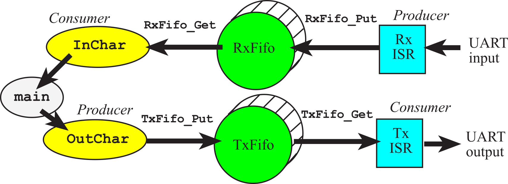
Figure 9.5.1. A data flow graph showing two FIFOs that buffer data between producers and consumers.
The flowchart for using two FIFOs is illustrated in Figure 9.5.2. With mailbox synchronization, the threads execute in lock-step: one, the other, one, the other… However, with the FIFO queue execution of the threads is more loosely coupled. The classic producer/consumer problem has two threads. One thread produces data and the other consumes data. For an input device, the background thread is the producer because it generates new data, and the foreground thread is the consumer because it uses the data up. For an output device, the data flows in the other direction so the producer/consumer roles are reversed. It is appropriate to pass data from the producer thread to the consumer thread using a FIFO queue
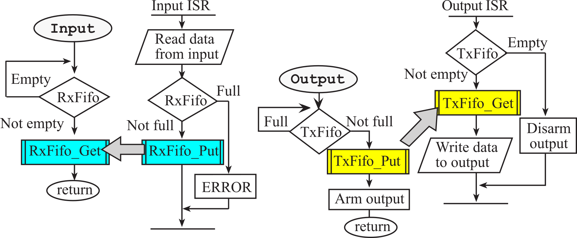
Figure 9.5.2. In a producer/consumer system, FIFO queues can be used to pass data between threads.
Details of the NVIC interrupts can be found back in Section
6.3. Refer to Section 6.3 to answer these next three
checkpoints:
: At what address is the UART1_Handler ISR vector?
: How do you arm UART1_Handler ISR in the NVIC?
: Where are the priority bits for the UART1 interrupt 6?
Figure 9.5.3 shows a data flow graph of Lab 9. Because the signals are encoded as voltages, the grounds must connected together. Figure 9.5.3 is classified as full-duplex, because transmission can occur in both directions simultaneously.

Figure 9.5.3. Lab 9 implements a full-duplex serial
communication channel.
Reprinted with approval from Introduction to Embedded Systems, 2022, ISBN: 978-1537105727

Embedded Systems - Shape the World by Jonathan Valvano and Ramesh Yerraballi is licensed under a Creative Commons Attribution-NonCommercial-NoDerivatives 4.0 International License.
Based on a work at http://users.ece.utexas.edu/~valvano/arm/outline1.htm.