Appendix
T. TM4C123 I/O Registers
Jonathan
Valvano and Mark McDermott
This chapter describes the TM4C123 I/O registers used in this book. It is not intended to replace the TM4C123 data sheet, but to serve as a quick reference for the specific registers used in this class.
Table of Contents:
- T.0. Nested Vectored Interrupt Controller (NVIC)
- T.1. GPIO and NVIC Programming
- T.2. ADC Programming
- T.3. Periodic Timer Interrupts
- T.4. UART
- T.5. Synchronous Transmission and Receiving using the SSI
- T.6. Inter-Integrated Circuit (I2C) Interface
- T.7. Edge-triggered Interrupts
- T.8. Pulse Width Modulation
- T.9. Input Capture
- T.10. Controller Area Network (CAN)
T.0. Nested Vectored Interrupt Controller (NVIC)
On the ARM Cortex-M microcontrollers, exceptions include resets, software interrupts and hardware interrupts. Interrupts on the Cortex-M are controlled by the Nested Vectored Interrupt Controller (NVIC). Each exception has an associated 32-bit vector that points to the interrupt service routine (ISR> that handles the exception. Vectors are stored in ROM at the beginning of memory. Program T.0.1 shows the first few vectors as defined in the Startup.s file. DCD is an assembler pseudo-op that defines a 32-bit constant. ROM location 0x00000000 has the initial stack pointer, and location 0x00000004 contains the initial program counter, which is called the reset vector. It points to a function called the reset handler, which is the first software executed following reset. There are up to 240 possible interrupt sources and their 32-bit vectors are listed in order starting with location 0x00000008. From a programming perspective, we can attach ISRs to interrupts by writing the ISRs as regular assembly subroutines or C functions with no input or output parameters and editing the Startup.s file to specify those functions for the appropriate interrupt. For example, if we wrote a Port F interrupt service routine named PortFISR, then we would replace GPIOPortF_Handler with PortFISR. In this book, we will define our ISRs using standard function names so that the Startup.s file need not be edited. I.e., we will simply name the ISR for edge-triggered interrupts on Port F as GPIOPortF_Handler. The ISR for this interrupt is a 32-bit pointer located at ROM address 0x000000B8. Because the vectors are in ROM, this linkage is defined at compile time and not at run time. For more details see the Startup.s files within the examples posted on the book web site.
: Where is the vector for SysTick? What is the standard name for this ISR?
EXPORT __Vectors
__Vectors ; address ISR
DCD StackMem + Stack ; 0x00000000 Top of Stack
DCD Reset_Handler ; 0x00000004 Reset Handler
DCD NMI_Handler ; 0x00000008 NMI Handler
DCD HardFault_Handler ; 0x0000000C Hard Fault Handler
DCD MemManage_Handler ; 0x00000010 MPU Fault Handler
DCD BusFault_Handler ; 0x00000014 Bus Fault Handler
DCD UsageFault_Handler ; 0x00000018 Usage Fault Handler
DCD 0 ; 0x0000001C Reserved
DCD 0 ; 0x00000020 Reserved
DCD 0 ; 0x00000024 Reserved
DCD 0 ; 0x00000028 Reserved
DCD SVC_Handler ; 0x0000002C SVCall Handler
DCD DebugMon_Handler ; 0x00000030 Debug Monitor Handler
DCD 0 ; 0x00000034 Reserved
DCD PendSV_Handler ; 0x00000038 PendSV Handler
DCD SysTick_Handler ; 0x0000003C SysTick Handler
DCD GPIOPortA_Handler ; 0x00000040 GPIO Port A
DCD GPIOPortB_Handler ; 0x00000044 GPIO Port B
DCD GPIOPortC_Handler ; 0x00000048 GPIO Port C
DCD GPIOPortD_Handler ; 0x0000004C GPIO Port D
DCD GPIOPortE_Handler ; 0x00000050 GPIO Port E
DCD UART0_Handler ; 0x00000054 UART0
DCD UART1_Handler ; 0x00000058 UART1
DCD SSI0_Handler ; 0x0000005C SSI
DCD I2C0_Handler ; 0x00000060 I2C
DCD PWM0Fault_Handler ; 0x00000064 PWM Fault
DCD PWM0Generator0_Handler ; 0x00000068 PWM 0 Generator 0
DCD PWM0Generator1_Handler ; 0x0000006C PWM 0 Generator 1
DCD PWM0Generator2_Handler ; 0x00000070 PWM 0 Generator 2
DCD Quadrature0_Handler ; 0x00000074 Quadrature Encoder 0
DCD ADC0Seq0_Handler ; 0x00000078 ADC0 Sequence 0
DCD ADC0Seq1_Handler ; 0x0000007C ADC0 Sequence 1
DCD ADC0Seq2_Handler ; 0x00000080 ADC0 Sequence 2
DCD ADC0Seq3_Handler ; 0x00000084 ADC0 Sequence 3
DCD WDT_Handler ; 0x00000088 Watchdog
DCD Timer0A_Handler ; 0x0000008C Timer 0 subtimer A
DCD Timer0B_Handler ; 0x00000090 Timer 0 subtimer B
DCD Timer1A_Handler ; 0x00000094 Timer 1 subtimer A
DCD Timer1B_Handler ; 0x00000098 Timer 1 subtimer B
DCD Timer2A_Handler ; 0x0000009C Timer 2 subtimer A
DCD Timer2B_Handler ; 0x000000A0 Timer 2 subtimer B
DCD Comp0_Handler ; 0x000000A4 Analog Comp 0
DCD Comp1_Handler ; 0x000000A8 Analog Comp 1
DCD Comp2_Handler ; 0x000000AC Analog Comp 2
DCD SysCtl_Handler ; 0x000000B0 System Control
DCD FlashCtl_Handler ; 0x000000B4 Flash Control
DCD GPIOPortF_Handler ; 0x000000B8 GPIO Port F
Program T.0.1. Software syntax to set the interrupt vectors for the TM4C (only some vectors are shown, see the startup.s file for a complete list).
Program T.0.2 shows that the syntax for an ISR looks like a function with no parameters. Notice that each ISR (except for SysTick) must acknowledge the interrupt in software by clearing the flag that caused the interrupt. In Program T.0.2, we assume the interrupt was caused by an edge on PF4, so writing to the ICR register will clear trigger flag 4.
void GPIOPortF_Handler(void){
GPIO_PORTF_ICR_R = 0x10; // ack, clear interrupt flag4
// stuff
}
Program T.0.2. Typical interrupt service routine.
|
Vector address |
Number |
IRQ |
ISR name in Startup.s |
NVIC |
Priority bits |
|
0x00000038 |
14 |
-2 |
PendSV_Handler |
NVIC_SYS_PRI3_R |
23 – 21 |
|
0x0000003C |
15 |
-1 |
SysTick_Handler |
NVIC_SYS_PRI3_R |
31 – 29 |
|
0x00000040 |
16 |
0 |
GPIOPortA_Handler |
NVIC_PRI0_R |
7 – 5 |
|
0x00000044 |
17 |
1 |
GPIOPortB_Handler |
NVIC_PRI0_R |
15 – 13 |
|
0x00000048 |
18 |
2 |
GPIOPortC_Handler |
NVIC_PRI0_R |
23 – 21 |
|
0x0000004C |
19 |
3 |
GPIOPortD_Handler |
NVIC_PRI0_R |
31 – 29 |
|
0x00000050 |
20 |
4 |
GPIOPortE_Handler |
NVIC_PRI1_R |
7 – 5 |
|
0x00000054 |
21 |
5 |
UART0_Handler |
NVIC_PRI1_R |
15 – 13 |
|
0x00000058 |
22 |
6 |
UART1_Handler |
NVIC_PRI1_R |
23 – 21 |
|
0x0000005C |
23 |
7 |
SSI0_Handler |
NVIC_PRI1_R |
31 – 29 |
|
0x00000060 |
24 |
8 |
I2C0_Handler |
NVIC_PRI2_R |
7 – 5 |
|
0x00000064 |
25 |
9 |
PWM0Fault_Handler |
NVIC_PRI2_R |
15 – 13 |
|
0x00000068 |
26 |
10 |
PWM0_Handler |
NVIC_PRI2_R |
23 – 21 |
|
0x0000006C |
27 |
11 |
PWM1_Handler |
NVIC_PRI2_R |
31 – 29 |
|
0x00000070 |
28 |
12 |
PWM2_Handler |
NVIC_PRI3_R |
7 – 5 |
|
0x00000074 |
29 |
13 |
Quadrature0_Handler |
NVIC_PRI3_R |
15 – 13 |
|
0x00000078 |
30 |
14 |
ADC0_Handler |
NVIC_PRI3_R |
23 – 21 |
|
0x0000007C |
31 |
15 |
ADC1_Handler |
NVIC_PRI3_R |
31 – 29 |
|
0x00000080 |
32 |
16 |
ADC2_Handler |
NVIC_PRI4_R |
7 – 5 |
|
0x00000084 |
33 |
17 |
ADC3_Handler |
NVIC_PRI4_R |
15 – 13 |
|
0x00000088 |
34 |
18 |
WDT_Handler |
NVIC_PRI4_R |
23 – 21 |
|
0x0000008C |
35 |
19 |
Timer0A_Handler |
NVIC_PRI4_R |
31 – 29 |
|
0x00000090 |
36 |
20 |
Timer0B_Handler |
NVIC_PRI5_R |
7 – 5 |
|
0x00000094 |
37 |
21 |
Timer1A_Handler |
NVIC_PRI5_R |
15 – 13 |
|
0x00000098 |
38 |
22 |
Timer1B_Handler |
NVIC_PRI5_R |
23 – 21 |
|
0x0000009C |
39 |
23 |
Timer2A_Handler |
NVIC_PRI5_R |
31 – 29 |
|
0x000000A0 |
40 |
24 |
Timer2B_Handler |
NVIC_PRI6_R |
7 – 5 |
|
0x000000A4 |
41 |
25 |
Comp0_Handler |
NVIC_PRI6_R |
15 – 13 |
|
0x000000A8 |
42 |
26 |
Comp1_Handler |
NVIC_PRI6_R |
23 – 21 |
|
0x000000AC |
43 |
27 |
Comp2_Handler |
NVIC_PRI6_R |
31 – 29 |
|
0x000000B0 |
44 |
28 |
SysCtl_Handler |
NVIC_PRI7_R |
7 – 5 |
|
0x000000B4 |
45 |
29 |
FlashCtl_Handler |
NVIC_PRI7_R |
15 – 13 |
|
0x000000B8 |
46 |
30 |
GPIOPortF_Handler |
NVIC_PRI7_R |
23 – 21 |
|
0x000000BC |
47 |
31 |
GPIOPortG_Handler |
NVIC_PRI7_R |
31 – 29 |
|
0x000000C0 |
48 |
32 |
GPIOPortH_Handler |
NVIC_PRI8_R |
7 – 5 |
|
0x000000C4 |
49 |
33 |
UART2_Handler |
NVIC_PRI8_R |
15 – 13 |
|
0x000000C8 |
50 |
34 |
SSI1_Handler |
NVIC_PRI8_R |
23 – 21 |
|
0x000000CC |
51 |
35 |
Timer3A_Handler |
NVIC_PRI8_R |
31 – 29 |
|
0x000000D0 |
52 |
36 |
Timer3B_Handler |
NVIC_PRI9_R |
7 – 5 |
|
0x000000D4 |
53 |
37 |
I2C1_Handler |
NVIC_PRI9_R |
15 – 13 |
|
0x000000D8 |
54 |
38 |
Quadrature1_Handler |
NVIC_PRI9_R |
23 – 21 |
|
0x000000DC |
55 |
39 |
CAN0_Handler |
NVIC_PRI9_R |
31 – 29 |
|
0x000000E0 |
56 |
40 |
CAN1_Handler |
NVIC_PRI10_R |
7 – 5 |
|
0x000000E4 |
57 |
41 |
CAN2_Handler |
NVIC_PRI10_R |
15 – 13 |
|
0x000000E8 |
58 |
42 |
Ethernet_Handler |
NVIC_PRI10_R |
23 – 21 |
|
0x000000EC |
59 |
43 |
Hibernate_Handler |
NVIC_PRI10_R |
31 – 29 |
|
0x000000F0 |
60 |
44 |
USB0_Handler |
NVIC_PRI11_R |
7 – 5 |
|
0x000000F4 |
61 |
45 |
PWM3_Handler |
NVIC_PRI11_R |
15 – 13 |
|
0x000000F8 |
62 |
46 |
uDMA_Handler |
NVIC_PRI11_R |
23 – 21 |
|
0x000000FC |
63 |
47 |
uDMA_Error |
NVIC_PRI11_R |
31 – 29 |
Table T.0.1. Some of the interrupt vectors for the TM4C. The TM4C123 has over 100 possible interrupt sources.
To activate an interrupt source we need to set its priority and enable that source in the NVIC. This activation is in addition to the arm and enable steps. Table T.0.1 lists some of the interrupt sources available on the TM4C family of microcontrollers. Interrupt numbers 0 to 15 contain the faults, software interrupt and SysTick; these interrupts will be handled differently from interrupts 16 and up.
Table T.0.2 shows some of the priority registers on the NVIC. Each register contains an 8-bit priority field for four devices. On the TM4C microcontrollers, only the top three bits of the 8-bit field are used. This allows us to specify the interrupt priority level for each device from 0 to 7, with 0 being the highest priority. The interrupt number (number column in Table T.0.1) is loaded into the IPSR register. The servicing of interrupts does not set the I bit in the PRIMASK, so a higher priority interrupt can suspend the execution of a lower priority ISR. If a request of equal or lower priority is generated while an ISR is being executed, that request is postponed until the ISR is completed. In particular, those devices that need prompt service should be given high priority.
|
Address |
31 – 29 |
23 – 21 |
15 – 13 |
7 – 5 |
Name |
|
0xE000E400 |
GPIO Port D |
GPIO Port C |
GPIO Port B |
GPIO Port A |
NVIC_PRI0_R |
|
0xE000E404 |
SSI0, Rx Tx |
UART1, Rx Tx |
UART0, Rx Tx |
GPIO Port E |
NVIC_PRI1_R |
|
0xE000E408 |
PWM Gen 1 |
PWM Gen 0 |
PWM Fault |
I2C0 |
NVIC_PRI2_R |
|
0xE000E40C |
ADC Seq 1 |
ADC Seq 0 |
Quad Encoder |
PWM Gen 2 |
NVIC_PRI3_R |
|
0xE000E410 |
Timer 0A |
Watchdog |
ADC Seq 3 |
ADC Seq 2 |
NVIC_PRI4_R |
|
0xE000E414 |
Timer 2A |
Timer 1B |
Timer 1A |
Timer 0B |
NVIC_PRI5_R |
|
0xE000E418 |
Comp 2 |
Comp 1 |
Comp 0 |
Timer 2B |
NVIC_PRI6_R |
|
0xE000E41C |
GPIO Port G |
GPIO Port F |
Flash Control |
System Control |
NVIC_PRI7_R |
|
0xE000E420 |
Timer 3A |
SSI1, Rx Tx |
UART2, Rx Tx |
GPIO Port H |
NVIC_PRI8_R |
|
0xE000E424 |
CAN0 |
Quad Encoder 1 |
I2C1 |
Timer 3B |
NVIC_PRI9_R |
|
0xE000E428 |
Hibernate |
Ethernet |
CAN2 |
CAN1 |
NVIC_PRI10_R |
|
0xE000E42C |
uDMA Error |
uDMA Soft Tfr |
PWM Gen 3 |
USB0 |
NVIC_PRI11_R |
|
0xE000ED20 |
SysTick |
PendSV |
-- |
Debug |
NVIC_SYS_PRI3_R |
Table T.0.2. The TM4C NVIC registers. Each register is 32 bits wide. Bits not shown are zero.
: Where are the priority bits for SysTick?
: Where are the priority bits for Timer 1A?
There are five enable registers NVIC_EN0_R through NVIC_EN4_R. The 32 bits in register NVIC_EN0_R control the IRQ numbers 0 to 31 (interrupt numbers 16 – 47). In Table T.0.1 we see UART0 is IRQ=5. To enable UART0 interrupts we set bit 5 in NVIC_EN0_R, see Table T.0.3. The 32 bits in NVIC_EN1_R control the IRQ numbers 32 to 63 (interrupt numbers 48 – 79). Not every interrupt source is available on every TM4C microcontroller, so you will need to refer to the data sheet for your microcontroller when designing I/O interfaces. Writing zeros to the NVIC_EN0_R through NVIC_EN4_R registers has no effect. To disable interrupts we write ones to the corresponding bit in the NVIC_DIS0_R through NVIC_DIS4_R register.
|
Address |
31 |
30 |
… |
6 |
5 |
4 |
3 |
2 |
1 |
0 |
Name |
|
0xE000E100 |
G |
F |
… |
UART1 |
UART0 |
E |
D |
C |
B |
A |
NVIC_EN0_R |
|
0xE000E104 |
|
|
… |
Quad1 |
I2C1 |
Timer3B |
Timer3A |
SSI1 |
UART2 |
H |
NVIC_EN1_R |
|
0xE000E180 |
G |
F |
… |
UART1 |
UART0 |
E |
D |
C |
B |
A |
NVIC_DIS0_R |
|
0xE000E184 |
|
|
… |
Quad1 |
I2C1 |
Timer3B |
Timer3A |
SSI1 |
UART2 |
H |
NVIC_DIS1_R |
Table T.0.3. Some of the TM4C NVIC interrupt enable registers. There are five such registers defining 139 interrupt enable bits.
: Where is the enable bit for UART2?
We can locate the enable bit for any interrupt using formulas. There are 32 enable bits in each register, so first we divide the IRQ number by 32. The modulus gives us the bit number. Let n be the IRQ number, from Table T.0.1.
x = n/32
m = n%32
The enable bit for interrupt IRQ=n is bit m of register NVIC_ENx_R. For example, Timer3A is IRQ=35, x=1, m=3. So, the enable bit for Timer3A is bit 3 of NVIC_EN1_R.
: Where is the enable bit for Timer 5A, IRQ=92?
Similarly, we can locate the priority bits for any interrupt using formulas. There are 4 sets of priority bits in each register, so first we divide the IRQ number by 4. The modulus helps us identify which bits are priority. Let n be the IRQ number, from Table T.0.1.
y = n/4
p = n%4
The priority bits for interrupt IRQ=n are bits 8*p+7, 8*p+6, 8*p+5 of register NVIC_PRIy_R. For example, Timer3A is IRQ=35, y=8, m=3. So, the priority bits for Timer3A are bits 31-29 of NVIC_PRI8_R.
: Where are the priority bits for Timer 4A, IRQ=70?
Interactive tool T.0.1 shows the context switch from executing in the foreground to running a periodic SysTick ISR. Before the interrupt occurs, the I bit in the PRIMASK is 0 signifying interrupts are enabled, and the interrupt number (ISRNUM) in the IPSR register is 0, meaning we are running in Thread mode (i.e., the main program, and not an ISR). Handler mode is signified by a nonzero value in IPSR. When BASEPRI register is zero, all interrupts are allowed and the BASEPRI register is not active.
When the SysTick counter goes from 1 to 0, the Count flag in the NVIC_ST_CTRL_R register is set, triggering an interrupt. The current instruction is finished. (a) Eight registers are pushed on the stack with R0 on top. These registers are pushed onto the stack . (b) The vector address is loaded into the PC (“Vector address” column in Table T.0.1). (c) The IPSR register is set to 15 (“Number” column in Table 12.1) (d) The top 24 bits of LR are set to 0xFFFFFF, signifying the processor is executing an ISR. The bottom eight bits specify how to return from interrupt.
0xE1 Return to Handler mode MSP (using floating point state on TM4C)
0xE9 Return to Thread mode MSP (using floating point state on TM4C)
0xED Return to Thread mode PSP (using floating point state on TM4C)
0xF1 Return to Handler mode MSP
0xF9 Return to Thread mode MSP ← in this class we will always be using this one
0xFD Return to Thread mode PSP
After pushing the registers, the processor always uses the main stack pointer (MSP) during the execution of the ISR. Events 2, 3, and 4 can occur simultaneously
Use the following tool to see the steps involved in a context switch from the executing the foreground thread to switching to the background thread (ISR) when a GPIOPortC_Handler interrupt occurs.
Click Start to start the context switch by pushing the current registers into the stack.
To return
from an interrupt, the ISR
executes the typical function return BX LR.
However, since the top 24 bits of LR
are 0xFFFFFF, it knows to return from interrupt by popping the eight
registers off the stack. Since the bottom eight bits of LR
in this case are 0b11111001, it returns to thread mode using the MSP
as its stack pointer. Since the IPSR
is part of the PSR
that is popped, it is automatically reset its previous state.
A nested interrupt occurs when a higher priority interrupt suspends an ISR. The lower priority interrupt will finish after the higher priority ISR completes. When one interrupt preempts another, the LR is set to 0xFFFFFFF1, so it knows to return to handler mode. Tail chaining occurs when one ISR executes immediately after another. Optimization occurs because the eight registers need not be popped only to be pushed once again. If an interrupt is triggered and is in the process of stacking registers when a higher priority interrupt is requested, this late arrival interrupt will be executed first.
Priority determines the order of service when two or more requests are made simultaneously. Priority also allows a higher priority request to suspend a lower priority request currently being processed. Usually, if two requests have the same priority, we do not allow them to interrupt each other. NVIC assigns a priority level to each interrupt trigger. This mechanism allows a higher priority trigger to interrupt the ISR of a lower priority request. Conversely, if a lower priority request occurs while running an ISR of a higher priority trigger, it will be postponed until the higher priority service is complete.
Observation: There are many interrupt sources, but an effective system will use only a few.
Program T.0.3 gives the definitions in startup.s that allow the software to enable and disable interrupts. These functions are callable from either assembly or C code. The wait for interrupt can be used to place the processor in low-power sleep mode while it waits for an interrupt.
;*********** DisableInterrupts ***************
; disable interrupts
; inputs: none
; outputs: none
DisableInterrupts CPSID I ;set I=1
BX LR
;*********** EnableInterrupts ***************
; enable interrupts
; inputs: none
; outputs: none
EnableInterrupts CPSIE I ;set I=0
BX LR
;*********** WaitForInterrupt ************************
; go to low power mode while waiting for the next interrupt
; inputs: none
; outputs: none
WaitForInterrupt
WFI
BX LR
Program T.0.3. Assembly functions needed for interrupt enabling and disabling.
T.1. GPIO Programming
T.1.1. I/O Registers
An I/O register is a location in memory with which software can interface with the I/O port. Initialization is executed once at the beginning. First, we turn on the clock in SYSCTL_RCGCGPIO_R by setting appropriate bits. Second, we wait about 25 ns, which is two bus cycles. Third, we write 1 into the corresponding DIR bit for each pin we wish to make output. Conversely we write a 0 into the corresponding DIR bit for each pin we wish to make input. To use the two switches on PF4 and PF0, we will also set bits 4 and 0 of the PUR register to activate an internal pull-up resistor. Lastly, we set the DEN bits to 1 to enable data pins. If we wish to input from a Port F GPIO pin we simply read from GPIO_PORTF_DATA_R. Reading from GPIO_PORTF_DATA_R obtains the current values for both input and output pins. If we wish to output to a Port F GPIO pin we write to GPIO_PORTF_DATA_R. Writing to GPIO_PORTF_DATA_R affects output pins but does not affect input pins. Table T.1.1 shows the addresses of some of the I/O registers.
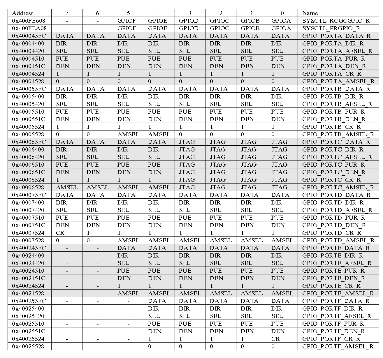
Table T.1.1. GPIO I/O registers.
: How does the software input from Port F?
: How does the software output to Port F?
We write to the PCTL register to set the mode of the pin, see Table T.1.2. Each pin has a 4-bit mode, as listed in Table T.1.3. In this section we will set the mode to 0000 to specify GPIO.
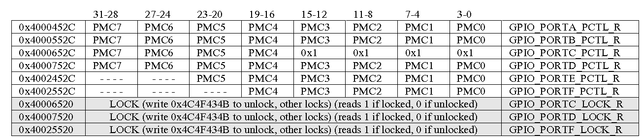
Table T.1.2. PCTL registers.
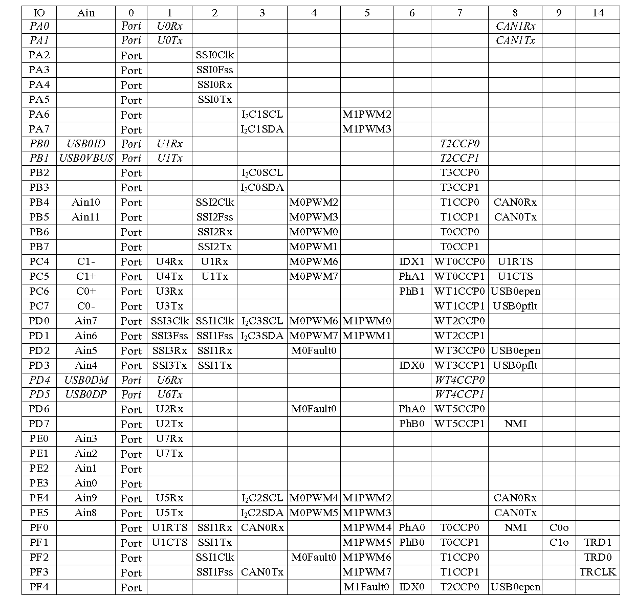
Table T.1.3. PCTL constants.
Each of the output pins can be configured to drive 2, 4, or 8 mA. There is one configuration for each output pin. Writing ones to the DR8R register will clear the corresponding bits in the DR2R and DR4R registers. I.e., each output pin will be 2, 4, or 8 mA.
GPIO_PORTA_DR2R_R // 2mA drive
GPIO_PORTA_DR4R_R // 4mA drive
GPIO_PORTA_DR8R_R // 8mA drive
GPIO_PORTB_DR2R_R // 2mA drive
GPIO_PORTB_DR4R_R // 4mA drive
GPIO_PORTB_DR8R_R // 8mA drive
GPIO_PORTC_DR2R_R // 2mA drive
GPIO_PORTC_DR4R_R // 4mA drive
GPIO_PORTC_DR8R_R // 8mA drive
GPIO_PORTD_DR2R_R // 2mA drive
GPIO_PORTD_DR4R_R // 4mA drive
GPIO_PORTD_DR8R_R // 8mA drive
GPIO_PORTE_DR2R_R // 2mA drive
GPIO_PORTE_DR4R_R // 4mA drive
GPIO_PORTE_DR8R_R // 8mA drive
GPIO_PORTF_DR2R_R // 2mA drive
GPIO_PORTF_DR4R_R // 4mA drive
GPIO_PORTF_DR8R_R // 8mA drive
To initialize a TM4C I/O port for general use we perform these steps. Because a hardware reset will assume digital GPIO, steps 4, 5 and 7 could be skipped. Only PD7 and PF0 on the TM4C123 need to be unlocked. All the other bits on the two microcontrollers are always unlocked. The direction register specifies bit for bit whether the corresponding pins are input (0) or output (1). PC3-0 are used by the debugger, so be friendly when accessing Port C.
- We activate the clock for the port.
- We wait 2 bus cycles for the clocks to stabilize.
- We unlock the pin if needed.
- We disable the analog function.
- We select GPIO mode (0000) in PCTL.
- We set its direction register.
- If an output, we set its drive current.
- We disable the alternate function.
- We enable the digital port.
T.1.2. Examples
In this first example, we interface a switch and LED to the TM4C123, see Figure T.1.1. We will make PD7 input, and we will make PD3 output, as shown in Program T.1.1. Notice each operation is friendly, meaning it only changes the bits needed, leaving the other bits unchanged. When we read GPIO_PORTD_DATA_R the bottom 8 bits are returned with the current values on Port D. The top 24 bits are returned zero. We select bit 7 by anding with 0x80. The Port_Input function returns a 0 or 1 depending on the input on PD7. The friendly output requires these steps.- We read the existing values from the data register into a temporary.
- We clear the bits we wish to change in the temporary.
- We combine the new bits with the old bits into the temporary.
- We write the temporary back to the data register
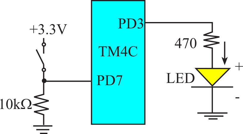
Figure T.1.1. Switch and LED interfaced to the TM4C123.
#define GPIO_PORTD_DATA_R (*((volatile uint32_t *)0x400073FC))
#define GPIO_PORTD_DIR_R (*((volatile uint32_t *)0x40007400))
#define GPIO_PORTD_AFSEL_R (*((volatile uint32_t *)0x40007420))
#define GPIO_PORTD_DEN_R (*((volatile uint32_t *)0x4000751C))
#define GPIO_PORTD_LOCK_R (*((volatile uint32_t *)0x40007520))
#define GPIO_PORTD_DR8R_R (*((volatile uint32_t *)0x40007508))
#define GPIO_PORTD_LOCK_R (*((volatile uint32_t *)0x40007520))
#define GPIO_PORTD_PCTL_R (*((volatile uint32_t *)0x4000752C))
#define SYSCTL_RCGCGPIO_R (*((volatile uint32_t *)0x400FE608))
#define SYSCTL_PRGPIO_R (*((volatile uint32_t *)0x400FEA08))
void Port_Init(void){
SYSCTL_RCGCGPIO_R |= 0x08; // 1) activate clock for Port D
while((SYSCTL_PRGPIO_R&0x08) == 0){};// 2) ready?
GPIO_PORTD_LOCK_R = 0x4C4F434B; // 3) unlock GPIO Port D
GPIO_PORTD_CR_R = 0xFF; // allow changes to PD7
GPIO_PORTD_AMSEL_R &= ~0x88; // 4) disable analog on PD7,PD3
GPIO_PORTD_PCTL_R = (GPIO_PORTD_PCTL_R&0x0FFF0FFF); // 5) PCTL GPIO on PD7,PD3
GPIO_PORTD_DIR_R &= ~0x80; // 6) PD7 in
GPIO_PORTD_DIR_R |= 0x08; // 6) PD3 out
GPIO_PORTD_DR8R_R |= 0x08; // 7) PD3 out, 8mA
GPIO_PORTD_AFSEL_R &= ~0x88; // 8) disable alt funct on PD7,PD3
GPIO_PORTD_DEN_R |= 0x88; // 9) enable digital I/O on PD7,PD3
}
uint32_t Port_Input(void){ // returns 0 or 1
return ((GPIO_PORTD_DATA_R&0x80)>>7); // read PD7 input
}
void Port_Output(uint32_t data){ // data is 0 or 1
GPIO_PORTD_DATA_R = (GPIO_PORTD_DATA_R&~0x08)|(data<<3); // write PD3 output
}
Program T.1.1. A set of functions using PD7 as input and PD3 as output.
Observation: Remember to enable the high current drive functionality on the GPIO output pin when interfacing an LED by setting the corresponding bits in the DR8R register.
There is no conflict if two or more modules enable the clock for Port D. There are two ways on the TM4C123 to access individual port bits. The first method is to use read-modify-write software to change just pin 3. A read-or-write sequence can be used to set one or more bits.
GPIO_PORTD_DATA_R |= 0x08; // make PD3 high
A read-and-write sequence can be used to clear one or more bits.
GPIO_PORTD_DATA_R &= ~0x08; // make PD3 low
T.1.3. Bit-specific addressing
The second method uses the bit-specific addressing.
The TM4C family implements a more flexible way to access port pins
than the bit-banding described earlier.
This bit-specific addressing doesn't work for all the I/O registers,
just the parallel port data registers.
The TM4C mechanism allows collective access to 1 to 8 bits in a data port.
We define eight address offset constants in Table T.1.4.
Basically, if we are interested in bit b, the constant is 4*2b.
There are 256 possible bit combinations we might be interested in accessing,
from all of them to none of them.
Each possible bit combination has a separate address
for accessing that combination.
For each bit we are interested in, we add up the corresponding constants
from Table T.1.4 and then add that sum to the base address for the port.
The base addresses for the data ports are listed in Table T.1.5.
For example, assume we are interested in Port A bits 1, 2, and 3.
The base address for Port A is 0x40004000, and the constants are 0x0020, 0x0010 and 0x008.
The sum of 0x40004000+0x0020+0x0010+0x008 is the address 0x40004038.
If we read from 0x40004038 only bits 1, 2, and 3 will be returned.
If we write to this address only bits 1, 2, and 3 will be modified.
|
Bit |
Constant |
|
7 |
0x0200 |
|
6 |
0x0100 |
|
5 |
0x0080 |
|
4 |
0x0040 |
|
3 |
0x0020 |
|
2 |
0x0010 |
|
1 |
0x0008 |
|
0 |
0x0004 |
Table T.1.4. Address offsets used to specify individual data port bits.
|
Port |
Address |
|
Port A |
0x40004000 |
|
Port B |
0x40005000 |
|
Port C |
0x40006000 |
|
Port D |
0x40007000 |
|
Port E |
0x40024000 |
|
Port F |
0x40025000 |
Table T.1.5. Base addresses of GPIO ports.
The base address for Port D is 0x40007000. If we want to read and write all 8 bits of this port, the constants will add up to 0x03FC. Notice that the sum of the base address and the constants yields the 0x400073FC address used in Program T.2.1. In other words, read and write operations to GPIO_PORTD_DATA_R will access all 8 bits of Port D. If we are interested in just bit 3 of Port D, we add 0x0020 to 0x40007000, and we can define this in C as
#define PD3 (*((volatile uint32_t *)0x40007020))
Now, a simple write operation can be used to set PD3.
The following code is friendly because it does not modify the other 7 bits of Port D.
PD3 = 0x08; // make PD3 high
A simple write sequence will clear PD3.
The following code is also friendly.
PD3 = 0x00; // make PD3 low
A read from PD3 will return 0x03 or 0x00
depending on whether the pin is high or low, respectively.
The following code is also friendly.
PD3 = PD3^0x08; // toggle PD3
: What happens if we write to location 0x40007000?
: Specify a #define that allows us to access bits 7 and 2 of Port D. Use this #define to make both bits 7 and 2 of Port D high.
: What happens if we write to location 0x40007000? Specify a #define that allows us to access bits 6, 5, 0 of Port B. Use this #define to make bits 6, 5 and 0 of Port B high.
In this next example, we will create debugging heartbeats. We will use bit-specific addressing so the code will have no critical sections (thread safe).
#define PD0 (*((volatile uint32_t *)0x40007004))
#define PD1 (*((volatile uint32_t *)0x40007008))
void Debug_Init(void){
SYSCTL_RCGCGPIO_R |= 0x08; // 1) activate clock for Port D
while((SYSCTL_PRGPIO_R&0x08) == 0){};// 2) ready?
GPIO_PORTD_LOCK_R = 0x4C4F434B; // 3) unlock GPIO Port D
GPIO_PORTD_CR_R = 0xFF; // allow changes
GPIO_PORTD_AMSEL_R &= ~0x03; // 4) disable analog on PD1,PD0
GPIO_PORTD_PCTL_R = (GPIO_PORTD_PCTL_R&0xFFFFFF00); // 5) PCTL GPIO on PD1,PD0
GPIO_PORTD_DIR_R |= 0x03; // 6) PD1,PD0 out
GPIO_PORTD_DR8R_R |= 0x03; // 7) PD1,PD0 out, 8mA
GPIO_PORTD_AFSEL_R &= ~0x03; // 8) disable alt funct on PD1,PD0
GPIO_PORTD_DEN_R |= 0x03; // 9) enable digital I/O on PD1,PD0
}
#define Debug_HeartBeat0() (PD0 ^= 0x01)
#define Debug_HeartBeat1() (PD1 ^= 0x02)
Program T.1.2. An LED monitor.
Let's consider why using bit-specific addressing removes critical sections. Both GPIO_PORTD_DATA_R ^= 0x02; and PD2 ^= 0x02; will toggle bit 1 in the 32-bit Port D data register. They both perform a read modify write sequence to create the toggle. They both create similar assembly code when compiled, as shown in Program T.1.3.
|
; GPIO_PORTD_DATA_R ^= 0x02; |
; PD2 ^= 0x02; |
Program T.1.3. Assembly code to toggle PD1.
Using GPIO_PORTD_DATA_R creates a critical section between the second and fourth assembly instructions. Reading GPIO_PORTD_DATA_R gives all of port D, and writing GPIO_PORTD_DATA_R changes all of port D. Assume some other thread interrupts this thread between the second and third (or between the third and fourth) instructions, and that other thread changes bits 7-2 or bit 0 in port D. When the other thread returns from interrupt, the value in R0 of this thread is the previous contents of bits 7-2 and bit 0. Therefore, the change made by the other interrupt is undone.
Using PD1 does not create a critical section. Reading PD1 gives just port D bit 1 (0 or 2), and writing PD1 only changes bit 1 of port D. Since the write to PD1 does not change bits 7-2 and bit 0, any changes caused by other interrupts will not be undone.
T.1.4. Keyboard Scanning
This matrix keyboard divides the sixteen keys into four rows and four columns, as shown in Figure T.1.2. Each key exists at a unique row/column location. It will take eight I/O pins to interface the rows and columns. Any output port on the TM4C could have been used to interface the rows. To scan the matrix, the software will drive the rows one at a time with open collector logic then read the columns. The open collector logic, with outputs HiZ and 0, will be created by toggling the direction register on the four rows. Actual 10 kΩ pull-up resistors will be placed on the column inputs (PA5-PA2) rather than configured internally, because the internal pull-ups are not fast enough to handle the scanning procedure.
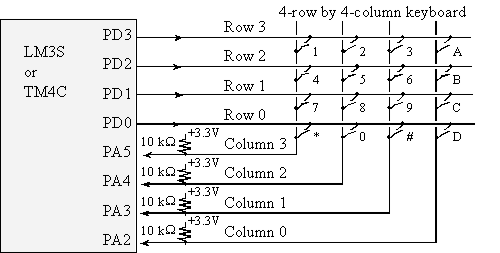
Figure T.1.2. A matrix keyboard interfaced to the microcontroller.
Program T.1.4 shows the initialization software. The data structure will assist in the scanning algorithm, and it provides a visual mapping from the physical layout of the keys to the ASCII code produced when touching that key. The structure also makes it easy to adapt this solution to other keyboard interfaces. A periodic interrupt can be used to debounce the switches. The key to debouncing is to not observe the switches more frequently than once every 10 ms.
void MatrixKeypad_Init(void){
SYSCTL_RCGCGPIO_R |= 0x09; // 1) activate clock for Ports A and D
while((SYSCTL_PRGPIO_R&0x09) != 0x09){};// ready?
GPIO_PORTA_AFSEL_R &= ~0x3C; // GPIO function on PA5-2
GPIO_PORTA_AMSEL_R &= ~0x3C; // disable analog function on PA5-2
GPIO_PORTA_PCTL_R &= ~0x00FFFF00; // configure PA5-2 as GPIO
GPIO_PORTA_DEN_R |= 0x3C; // enable digital I/O on PA5-2
GPIO_PORTA_DIR_R &= ~0x3C; // make PA5-2 in (PA5-2 columns)
GPIO_PORTD_AFSEL_R &= ~0x0F; // GPIO function on PD3-0
GPIO_PORTD_AMSEL_R &= ~0x0F; // disable analog function on PD3-0
GPIO_PORTD_PCTL_R &= ~0x0000FFFF; // configure PD3-0 as GPIO
GPIO_PORTD_DATA_R &= ~0x0F; // DIRn=0, OUTn=HiZ; DIRn=1, OUTn=0
GPIO_PORTD_DEN_R |= 0x0F; // enable digital I/O on PD3-0
GPIO_PORTD_DIR_R &= ~0x0F; // make PD3-0 in (PD3-0 rows)
GPIO_PORTD_DR8R_R |= 0x0F;} // enable 8 mA drive
Program T.1.4. Initialization software for a matrix keyboard.
Program T.1.5 shows the
scanning software. The scanning sequence is listed in Table T.1.6. There are
two steps to scan a particular row:
- Select that row by driving it low, while the other rows are HiZ,
- Wait for the circuit to stabilize
- Read the columns to see if any keys are pressed in that row,
- 0 means the key is pressed
- 1 means the key is not pressed
It is important to observe column and row signals on a dual trace oscilloscope while running the software at full speed, because it takes time for correct signal to appear on the column after the row is changed. In most cases, a software delay should be inserted between setting the row and reading the column. The length of the delay you will need depends on the size of the pull-up resistor and any stray capacitance that may exist in your circuit.
|
direction |
PD0 |
PD1 |
PD2 |
PD3 |
PA2 |
PA3 |
PA4 |
PA5 |
|
0x01 |
0 |
HiZ |
HiZ |
HiZ |
1 |
2 |
3 |
A |
|
0x02 |
HiZ |
0 |
HiZ |
HiZ |
4 |
5 |
6 |
B |
|
0x04 |
HiZ |
HiZ |
0 |
HiZ |
7 |
8 |
9 |
C |
|
0x08 |
HiZ |
HiZ |
HiZ |
0 |
* |
0 |
# |
D |
Table T.1.6. Patterns for a 4 by 4 matrix keyboard.
struct Row{
uint8_t direction;
char keycode[4];
};
typedef const struct Row Row_t;
Row_t ScanTab[5]={
{ 0x01, "123A" }, // row 0
{ 0x02, "456B" }, // row 1
{ 0x04, "789C" }, // row 2
{ 0x08, "*0#D" }, // row 3
{ 0x00, " " }
};
// Returns ASCII code for key pressed,
// Num is the number of keys pressed
// both equal zero if no key pressed
char MatrixKeypad_Scan(int32_t *Num){
Row_t *pt;
uint32_t column; char key;
uint32_t j;
(*Num) = 0;
key = 0; // default values
pt = &ScanTab[0];
while(pt->direction){
GPIO_PORTD_DIR_R = pt->direction; // one output
GPIO_PORTD_DATA_R &= ~0x0F; // DIRn=0, OUTn=HiZ; DIRn=1, OUTn=0
for(j=1; j<=10; j++); // very short delay
column = ((GPIO_PORTA_DATA_R&0x3C)>>2);// read columns
for(j=0; j<=3; j++){
if((column&0x01)==0){
key = pt->keycode[j];
(*Num)++;
}
column>>=1; // shift into position
}
pt++;
}
return key;
}
// Waits for a key to be pressed, then released
// returns ASCII code for key pressed,
// n is the number of keys pressed
// both equal zero if no key pressed */
char MatrixKeypad_In(void){ int32_t n;
char letter;
do{
letter = MatrixKeypad_Scan(&n);
} while (n != 1); // repeat until exactly one
do{
letter = MatrixKeypad_Scan(&n);
} while (n != 0); // repeat until release
return letter;
}
Program T.1.5. Scanning software for a matrix keyboard
Two-key rollover occurs when the operator is typing quickly. For example, if the operator is typing the A, B, then C, he/she might type A, AB, B, BC, C, and then release. With rollover, the keyboard does not go through a no-key state in between typing. The hardware interface in Figure T.1.2 could handle two-key rollover, but the software solution in Program T.1.5 does not.
One of the problems with switches is called switch bounce. Many inexpensive switches will mechanically oscillate for up to a few milliseconds when touched or released. It behaves like an underdamped oscillator. These mechanical oscillations cause electrical oscillations such that a port pin will oscillate high/low during the bounce. In some cases, this bounce should be removed.
There are two good solutions to using interrupt synchronization for the keyboard. The approach implemented here uses periodic polling, because it affords a simple solution to both bouncing and two-key rollover. The time between interrupts is selected to be longer than the maximum bounce time, but shorter than the minimum time between key strikes. If you type ten characters per second, the minimum time between rising and falling edges is about 50 ms. Since switch bounce times are less than 10 ms, we will poll the keyboard every 25 ms. This means the average latency will be 12.5 ms, and the maximum latency will be 25 ms.
The initialization include GPIO, SysTick, and a FIFO. A key is recognized if the scanning returns one key found, and this key is different from what it scanned 25 ms ago.
AddIndexFifo(Matrix, 16, char, 1, 0) // create a FIFO
char static LastKey;
void Matrix_Init(void){
LastKey = 0; // no key typed
MatrixFifo_Init();
MatrixKeypad_Init();
SysTick_Init(1250000); // 25 ms polling
}
void SysTick_Handler(void){ char thisKey; int32_t n;
thisKey = MatrixKeypad_Scan(&n); // scan
if((thisKey != LastKey) && (n == 1)){
MatrixFifo_Put(thisKey);
LastKey = thisKey;
} else{
LastKey = 0; // invalid
}
}
char Matrix_InChar(void){ char letter;
while(MatrixFifo_Get(&letter) == FIFOFAIL){};
return(letter);
}
Program T.1.5. Periodic polling interface of a scanned keyboard.
One of the advantages of Program T.1.5 is two-key rollover. When people type very fast, they sometimes type the next key before the release the first key. For example, when the operator types the letters "BCD" slowly with one finger, the keyboard status goes in this sequence
<none>, <B>, <none>, <C>, <none>, <D>, <none>
Conversely, if the operator types quickly, there can be two-key rollover, which creates this sequence
<none>, <B>, <BC>, <C>, <CD>, <D>, <none>
where <BC> means both keys 'B' and 'C' are touched. Two-key rollover means the keyboard does not go through a state where no keys are touched between typing the 'B' and the 'C'. Since each of the keys goes through a state where exactly one key is pressed and is different than it was 25 ms ago, Program T.1.5 will handle two-key rollover.
A second approach is to arm the device for interrupts by driving all rows to zero. In this manner, we will receive a falling edge on one of the Port A inputs when any key is touched. During the ISR we could scan the keyboard and put the key into the FIFO. To solve the bounce problem this solution implements a time delay from key touch to when the software scans for keys. This approach uses a combination of edge-triggered inputs and timer interrupts to perform input in the background. When arming for interrupts, we set all four rows to output zero. In this way, a falling edge interrupt will occur on any key touched. When an edge-triggered interrupt occurs, we will disarm this input and arm an timer to trigger in 10 ms. It is during the timer ISR we scan the matrix. If there is exactly one key, we enter it into the FIFO. An interrupt may occur on release due to bounce. However, 10 ms after the release, when we scan during the Timer0A_Handler the MatrixKeypad_Scan function will return a Num of zero, and we will ignore it. This solution solves switch bounce, but not two-key rollover.
There are three solutions to debounce an individual switch
1) Blind synchronization: read switch, and then wait 10 ms
2) Periodic polling: use a periodic interrupt at 10 ms
3) Interrupt:
edge-triggered interrupt, then time delay interrupt
Table T.2.1 shows the ADC0 register bits required to perform sampling on a single channel. Any bits not specified will read 0. There are two ADCs; you will use ADC0 and TExaSdisplay uses ADC1. For more complex configurations refer to the specific data sheet. The value in the ADC0_PC_R specifies the maximum sampling rate, see Table T.2.2. This is not the actual sampling rate; it is the maximum possible. Setting ADC0_PC_R to 7, allows the TM4C123 to sample up to 1 million samples per second. The example code in this section will set ADC0_PC_R to 1, because we will be sampling much slower than 125 kHz. It will be more accurate and require less power to run at 125 kHz maximum mode, as compared to 1 MHz maximum mode. In this chapter we will use software trigger mode, so the actual sampling rate is determined by the SysTick periodic interrupt rate; the SysTick ISR will take one ADC sample. On the TM4C123, we will need to set bits in the AMSEL register to activate the analog interface. Furthermore, we will clear bits DEN register to deactivate the digital interface.
|
Address |
31-17 |
16 |
15-3 |
|
2 |
1 0 |
Name |
||
|
0x400F.E638 |
|
|
|
|
ADC1 ADC0 |
SYSCTL_RCGCADC_R |
|||
|
|
|
|
|
|
|
|
|
|
|
|
|
31-14 |
13-12 |
11-10 |
9-8 |
7-6 |
5-4 |
3-2 |
1-0 |
|
|
0x4003.8020 |
|
SS3 |
|
SS2 |
|
SS1 |
|
SS0 |
ADC0_SSPRI_R |
|
|
|
|
|
|
|
|
|
|
|
|
|
31-16 |
15-12 |
11-8 |
7-4 |
3-0 |
|
|||
|
0x4003.8014 |
|
EM3 |
EM2 |
EM1 |
EM0 |
ADC0_EMUX_R |
|||
|
|
|
|
|
|
|
|
|
|
|
|
|
31-4 |
3 |
2 |
1 |
0 |
|
|||
|
0x4003.8000 |
|
ASEN3 |
ASEN2 |
ASEN1 |
ASEN0 |
ADC0_ACTSS_R |
|||
|
0x4003.8030 |
|
AVE (3 bits) |
ADC0_SAC_R |
||||||
|
0x4003.80A0 |
|
MUX0 |
ADC0_SSMUX3_R |
||||||
|
0x4003.8FC4 |
|
Speed |
ADC0_PC_R |
||||||
|
0x4003.80A4 |
|
TS0 |
IE0 |
END0 |
D0 |
ADC0_SSCTL3_R |
|||
|
0x4003.8028 |
|
SS3 |
SS2 |
SS1 |
SS0 |
ADC0_PSSI_R |
|||
|
0x4003.8004 |
|
INR3 |
INR2 |
INR1 |
INR0 |
ADC0_RIS_R |
|||
|
0x4003.800C |
|
IN3 |
IN2 |
IN1 |
IN0 |
ADC0_ISC_R |
|||
|
|
|
|
|
|
|
|
|
|
|
|
|
31-12 |
11-0 |
|
||||||
|
0x4003.80A8 |
|
DATA |
ADC0_SSFIFO3 |
||||||
Table T.2.1. The TM4C ADC registers. Each register is 32 bits wide. You will use ADC0 and we will use ADC1 to implement the oscilloscope feature.
|
Value |
Description |
|
0x7 |
1M samples/second |
|
0x5 |
500K samples/second |
|
0x3 |
250K samples/second |
|
0x1 |
125K samples/second |
Table T.2.2. The maximum sampling rate specified in the ADC0_PC_R register.
Table T.2.3 shows which I/O pins on the TM4C123 can be used for ADC analog input channels.
|
IO |
Ain |
0 |
1 |
2 |
3 |
4 |
5 |
6 |
7 |
8 |
9 |
14 |
|
PB4 |
Ain10 |
Port |
|
SSI2Clk |
|
M0PWM2 |
|
|
T1CCP0 |
CAN0Rx |
|
|
|
PB5 |
Ain11 |
Port |
|
SSI2Fss |
|
M0PWM3 |
|
|
T1CCP1 |
CAN0Tx |
|
|
|
PD0 |
Ain7 |
Port |
SSI3Clk |
SSI1Clk |
I2C3SCL |
M0PWM6 |
M1PWM0 |
|
WT2CCP0 |
|
|
|
|
PD1 |
Ain6 |
Port |
SSI3Fss |
SSI1Fss |
I2C3SDA |
M0PWM7 |
M1PWM1 |
|
WT2CCP1 |
|
|
|
|
PD2 |
Ain5 |
Port |
SSI3Rx |
SSI1Rx |
|
M0Fault0 |
|
|
WT3CCP0 |
USB0epen |
|
|
|
PD3 |
Ain4 |
Port |
SSI3Tx |
SSI1Tx |
|
|
|
IDX0 |
WT3CCP1 |
USB0pflt |
|
|
|
PE0 |
Ain3 |
Port |
U7Rx |
|
|
|
|
|
|
|
|
|
|
PE1 |
Ain2 |
Port |
U7Tx |
|
|
|
|
|
|
|
|
|
|
PE2 |
Ain1 |
Port |
|
|
|
|
|
|
|
|
|
|
|
PE3 |
Ain0 |
Port |
|
|
|
|
|
|
|
|
|
|
|
PE4 |
Ain9 |
Port |
U5Rx |
|
I2C2SCL |
M0PWM4 |
M1PWM2 |
|
|
CAN0Rx |
|
|
|
PE5 |
Ain8 |
Port |
U5Tx |
|
I2C2SDA |
M0PWM5 |
M1PWM3 |
|
|
CAN0Tx |
|
|
Table T.2.3. Twelve different pins on the TM4C123 can be used to sample analog inputs. The example code will use ADC0 and PE4/Ch9 to sample analog input. TExaSdisplay uses ADC1 and PD3 to implement the oscilloscope feature.
The ADC has four sequencers. We set the ADC0_SSPRI_R register to 0x0123 to make sequencer 3 the highest priority. Because we are using just one sequencer, we just need to make sure each sequencer has a unique priority. We set bits 15-12 (EM3) in the ADC0_EMUX_R register to specify how the ADC will be triggered. Table T.2.4 shows the various ways to trigger an ADC conversion. Timer-triggered ADC sampling (EM3=0x5) has very low jitter. However, we will begin with software triggering (EM3=0x0). The software writes an 8 (SS3) to the ADC0_PSSI_R to initiate a conversion on sequencer 3. We can enable and disable the sequencers using the ADC0_ACTSS_R register. There are twelve ADC channels on the TM4C123. Which channel we sample is configured by writing to the ADC0_SSMUX3_R register. The mapping between channel number and the port pin is shown in Table T.2.3. For example channel 9 is connected to the pin PE4. The ADC0_SSCTL3_R register specifies the mode of the ADC sample. We set TS0 to measure temperature and clear it to measure the analog voltage on the ADC input pin. We set IE0 so that the INR3 bit is set when the ADC conversion is complete, and clear it when no flags are needed. When using sequencer 3, there is only one sample, so END0 will always be set, signifying this sample is the end of the sequence. In this class, the sequence will be just one ADC conversion. We set the D0 bit to activate differential sampling, such as measuring the analog difference between two ADC pins. In our example, we clear D0 to sample a single-ended analog input. Because we set the IE0 bit, the INR3 flag in the ADC0_RIS_R register will be set when the ADC conversion is complete, We clear the INR3 bit by writing an 8 to the ADC0_ISC_R register.
|
Value |
Event |
|
0x0 |
Software start |
|
0x1 |
Analog Comparator 0 |
|
0x2 |
Analog Comparator 1 |
|
0x3 |
Analog Comparator 2 |
|
0x4 |
External (GPIO PB4) |
|
0x5 |
Timer |
|
0x6 |
PWM0 |
|
0x7 |
PWM1 |
|
0x8 |
PWM2 |
|
0x9 |
PWM3 |
|
0xF |
Always (continuously sample) |
Table T.2.4. The ADC EM3, EM2, EM1, and EM0 bits in the ADC_EMUX_R register.
We perform the following steps to configure the ADC for software start on one channel. Program T.2.1 shows a specific details for sampling PE4, which is channel 9. The function ADC0_InSeq3 will sample PE4 using software start and use busy-wait synchronization to wait for completion.
Step 1. We enable the ADC clock bit 0 in SYSCTL_RCGCADC_R for ADC0.
Step 2. We enable the port clock for the pin that we will be using for the ADC input.
Step 3. We wait for the two clocks to stabilize (some people found extra delay prevented hard faults)
Step 4. Make that pin an input by writing zero to the DIR register.
Step 5. Enable the alternative function on that pin by writing one to the AFSEL register.
Step 6. Disable the digital function on that pin by writing zero to the DEN register.
Step 7. Enable the analog function on that pin by writing one to the AMSEL register.
Step 8. We set the ADC0_PC_R register specify the maximum sampling rate of the ADC. In this example, we will sample slower than 125 kHz, so the maximum sampling rate is set at 125 kHz. This will require less power and produce a longer sampling time, creating a more accurate conversion.
Step 9. We will set the priority of each of the four sequencers. In this case, we are using just one sequencer, so the priorities are irrelevant, except for the fact that no two sequencers should have the same priority.
Step 10. Before configuring the sequencer, we need to disable it. To disable sequencer 3, we write a 0 to bit 3 (ASEN3) in the ADC0_ACTSS_R register. Disabling the sequencer during programming prevents erroneous execution if a trigger event were to occur during the configuration process.
Step 11. We configure the trigger event for the sample sequencer in the ADC0_EMUX_R register. For this example, we write a 0000 to bits 15-12 (EM3) specifying software start mode for sequencer 3.
Step 12. Configure the corresponding input source in the ADC0_SSMUX3 register. In this example, we write the channel number to bits 3-0 in the ADC0_SSMUX3_R register. In this example, we sample channel 9, which is PE4.
Step 13. Configure the sample control bits in the corresponding nibble in the ADC0_SSCTL3 register. When programming the last nibble, ensure that the END bit is set. Failure to set the END bit causes unpredictable behavior. Sequencer 3 has only one sample, so we write a 0110 to the ADC0_SSCTL3_R register. Bit 3 is the TS0 bit, which we clear because we are not measuring temperature. Bit 2 is the IE0 bit, which we set because we want to the RIS bit to be set when the sample is complete. Bit 1 is the END0 bit, which is set because this is the last (and only) sample in the sequence. Bit 0 is the D0 bit, which we clear because we do not wish to use differential mode.
Step 14. Disable interrupts in ADC by clearing bits in the ADC0_IM_R register. Since we are using sequencer 3, we disable SS3 interrupts by clearing bit 3.
Step 15. We enable the sample sequencer logic by writing a 1 to the corresponding ASEN3. To enable sequencer 3, we write a 1 to bit 3 (ASEN3) in the ADC0_ACTSS_R register.
void ADC0_InitSWTriggerSeq3_Ch9(void){
SYSCTL_RCGCADC_R |= 0x0001; // 1)
activate ADC0
SYSCTL_RCGCGPIO_R |= 0x10; // 2)
activate clock for Port E
while((SYSCTL_PRGPIO_R&0x10) != 0x10){}; // 3
for stabilization
GPIO_PORTE_DIR_R &= ~0x10; //
4) make PE4 input
GPIO_PORTE_AFSEL_R |= 0x10; // 5)
enable alternate function on PE4
GPIO_PORTE_DEN_R &= ~0x10; //
6) disable digital I/O on PE4
GPIO_PORTE_AMSEL_R |= 0x10; // 7)
enable analog functionality on PE4
// while((SYSCTL_PRADC_R&0x0001) != 0x0001){}; // good code, but
not implemented in simulator
ADC0_PC_R &= ~0xF;
ADC0_PC_R |=
0x1; //
8) configure for 125K samples/sec
ADC0_SSPRI_R =
0x0123; // 9)
Sequencer 3 is highest priority
ADC0_ACTSS_R &=
~0x0008; // 10) disable sample
sequencer 3
ADC0_EMUX_R &=
~0xF000; // 11) seq3 is
software trigger
ADC0_SSMUX3_R &= ~0x000F;
ADC0_SSMUX3_R +=
9; //
12) set channel
ADC0_SSCTL3_R =
0x0006; // 13) no TS0 D0,
yes IE0 END0
ADC0_IM_R &=
~0x0008; // 14)
disable SS3 interrupts
ADC0_ACTSS_R |=
0x0008; // 15) enable
sample sequencer 3
}
Program T.2.1. Initialization of the ADC using software start and busy-wait (ADCSWTrigger).
Video T.2.1. ADC Initialization Ritual
Program T.2.2 gives a function that performs an ADC conversion. There are four steps required to perform a software-start conversion. The range is 0 to 3.3V. If the analog input is 0, the digital output will be 0, and if the analog input is 3.3V, the digital output will be 4095.
Digital Sample = (Analog Input (volts) • 4095) / 3.3V(volts)
Step 1. The ADC is started using the software trigger. The channel to sample was specified earlier in the initialization.
Step 2. The function waits for the ADC to complete by polling the RIS register bit 3.
Step 3. The 12-bit digital sample is read out of sequencer 3.
Step 4. The RIS bit is cleared by writing to the ISC register.
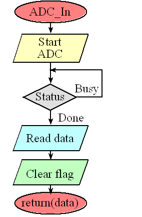
Figure T.2.3. The four steps of analog to digital conversion: 1) initiate conversion, 2) wait for the ADC to finish, 3) read the digital result, and 4) clear the completion flag.
//------------ADC0_InSeq3------------
// Busy-wait analog to digital conversion
// Input: none
// Output: 12-bit result of ADC conversion
uint32_t ADC0_InSeq3(void){ uint32_t result;
ADC0_PSSI_R = 0x0008; // 1) initiate SS3
while((ADC0_RIS_R&0x08)==0){}; // 2) wait for conversion done
result = ADC0_SSFIFO3_R&0xFFF; // 3) read result
ADC0_ISC_R = 0x0008; // 4) acknowledge completion
return result;
}
Program T.2.2. ADC sampling using software start and busy-wait (ADCSWTrigger).
Video T.2.2. Capturing a Sample
: If the input voltage is 1.65V, what value will the TM4C 12-bit ADC return?
: If the input voltage is 1.0V, what value will the TM4C 12-bit ADC return?
It is important to sample the ADC at a regular rate. One simple way to deploy periodic sampling is to perform the ADC conversion in a periodic ISR. In Program T.2.3, the sampling rate is determined by the rate of the periodic interrupt. The global variable, Flag is called a semaphore, which is set when new information is stored into the variable Data. We can connect PD0 to a logic analyzer or oscilloscope to verify the sampling rate. Triple toggling allows us to measure the execution time of the ISR and the time between ISR invocations.
uint32_t Data; // 0 to 4095
uint32_t Flag; // 1 means new data
void SysTick_Handler(void){
Debug_HeartBeat0(); // toggle PD0
Debug_HeartBeat0(); // toggle PD0
Data =
ADC0_InSeq3(); // Sample ADC
Flag =
1; //
Synchronize with other threads
Debug_HeartBeat0(); // toggle PD0
}
Program T.2.3. Real-time sampling using SysTick Interrupts.
Observation: The triple toggle technique allows us to measure the execution time of the ISR (second to third toggle) and the time between interrupts (first toggle to the next first toggle).
Next, we will configure the ADC to sample a single channel at a periodic rate using a timer trigger. The most time-accurate sampling method is timer-triggered sampling (EM3=0x5). There is virtually no sampling jitter because the hardware timer starts the ADC conversion. When the software runs the ISR does not affect when the data was sampled.
: If the bus clock is 80 MHz and the SysTick LOAD register is 79999, what will be the ADC sampling rate?
: If the bus clock is 80 MHz and we wish to sample at 10 kHz, what value do we write into the SysTick LOAD register?
There are 13 steps to configure the ADC to sample a single channel at a periodic rate. The most accurate sampling method is timer-triggered sampling (EM3=0x5). On the TM4C123, the MUX fields are 4 bits wide, allowing us to specify channels 0 to 11. Timer-triggered sampling will have zero sampling jitter because the hardware starts each sample.
Step 1. We enable the ADC clock in the SYSCTL_RCGCADC_R register.
Step 2. Bits 3-0 of the ADC0_PC_R register specify the maximum sampling rate of the ADC. The actual sampling rate is determined by how fast the ADC is triggered. Running at 125 kHz will require less power and produce a longer sampling time compared to the faster modes, creating a more accurate conversion.
Step 3. We will set the priority of each of the four sequencers. In this case, we are using just one sequencer, so the priorities are irrelevant, except for the fact that no two sequencers should have the same priority.
Step 4. Next, we need to configure the timer to run at the desired sampling frequency. We enable the Timer0 clock by setting bit 0 of the SYSCTL_RCGCTIMER_R register. This initialization is similar to Program T.2.3 with two changes. First we set bit 5 of the TIMER0_CTL_R register to activate TAOTE, which is the Timer A output trigger enable. Secondly, we do not arm any Timer0 interrupts. The rate at which the timer rolls over determines the sampling frequency. Let prescale be the value loaded into TIMER0_TAPR_R, and let period be the value loaded into TIMER0_TAILR_R. If the period of the bus clock frequency is Δt, then the ADC sampling period will be Δt *(prescale + 1)*(period + 1)
The fastest sampling rate is determined by the speed of the processor handling the ADC interrupts and by the speed of the main program consuming the data from the FIFO. If the bus clock is 80 MHz, the slowest possible sampling rate for this example is 80MHz/232, which is about 0.018 Hz, which is every 53 seconds.
Step 5. Before configuring the sequencer, we need to disable it. To disable sequencer 3, we write a 0 to bit 3 (ASEN3) in the ADC0_ACTSS_R register. Disabling the sequencer during programming prevents erroneous execution if a trigger event were to occur during the configuration process.
Step 6. We configure the trigger event for the sample sequencer in the ADC0_EMUX_R register. For this example, we write a 0101 to bits 15-12 (EM3) specifying timer trigger mode for sequencer 3.
Step 7. For each sample in the sample sequence, configure the corresponding input source in the ADC0_SSMUXn register. In this example, we write the channel number (0, 1, 2, or 3) to bits 3-0 in the ADC0_SSMUX3_R register.
Step 8. For each sample in the sample sequence, we configure the sample control bits in the corresponding nibble in the ADC0_SSCTLn register. When programming the last nibble, ensure that the END bit is set. Failure to set the END bit causes unpredictable behavior. Sequencer 3 has only one sample, so we write a 0110 to the ADC0_SSCTL3_R register. Bit 3 is the TS0 bit, which we clear because we are not measuring temperature. Bit 2 is the IE0 bit, which we set because we want to request an interrupt when the sample is complete. Bit 1 is the END0 bit, which is set because this is the last (and only) sample in the sequence. Bit 0 is the D0 bit, which we clear because we do not wish to use differential mode.
Step 9. If interrupts are to be used, write a 1 to the corresponding mask bit in the ADC0_IM_R register. We want an interrupt to occur when the conversion is complete (set bit 3, MASK3).
Step 10. We enable the sample sequencer logic by writing a 1 to the corresponding ASENn. To enable sequencer 3, we write a 1 to bit 3 (ASEN3) in the ADC0_ACTSS_R register.
Step 11. The priority of the ADC0 sequencer 3 interrupts are in bits 13-15 of the NVIC_PRI4_R register.
Step 12. Since we are requesting interrupts, we need to enable interrupts in the NVIC. ADC sequencer 3 interrupts are enabled by setting bit 17 in the NVIC_EN0_R register.
Step 13. Lastly, we must enable interrupts in the PRIMASK register, which is typically done in the main program after all initializations are complete.
The timer starts the conversion at a regular rate. Bit 3 (INR3) in the ADC0_RIS_R register will be set when the conversion is done. This bit is armed and enabled for interrupting, so conversion complete will trigger an interrupt. The IN3 bit in the ADC0_ISC_R register triggers the interrupt. The ISR acknowledges the interrupt by writing a 1 to bit 3 (IN3). The 12-bit result is read from the ADC0_SSFIFO3_R register. The book web site for has example code. In order to reduce latency of other interrupt requests in the system, this ISR simply stores the 12-bit conversion in a FIFO, to be processed later in the main program. Programs T.2.4 and T.2.5 shows the initialization and interrupt service routine to affect the periodic sampling. For the port pin, we disable its DEN, clear its DIR, set its AFSEL and enable its AMSEL bit.
void (*ADCTask)(uint32_t); // user function to be called when new ADC data ready
void ADC0_InitTimer0ATriggerSeq3PD3(uint32_t period, void(*task)(uint32_t)){
volatile uint32_t delay;
SYSCTL_RCGCADC_R |= 0x01; // 1) activate ADC0
SYSCTL_RCGCGPIO_R |= 0x08; // Port D clock
delay = SYSCTL_RCGCGPIO_R; // allow time for clock to stabilize
GPIO_PORTD_DIR_R &= ~0x08; // make PD3 input
GPIO_PORTD_AFSEL_R |= 0x08; // enable alternate function on PD3
GPIO_PORTD_DEN_R &= ~0x08; // disable digital I/O on PD3
GPIO_PORTD_AMSEL_R |= 0x08; // enable analog functionality on PD3
ADC0_PC_R = 0x01; // 2) maximum speed is 125K samples/sec
ADC0_SSPRI_R = 0x3210; // 3) seq 0 is highest, seq 3 is lowest
SYSCTL_RCGCTIMER_R |= 0x01; // 4) activate timer0
delay = SYSCTL_RCGCGPIO_R;
TIMER0_CTL_R = 0x00000000; // disable timer0A during setup
TIMER0_CTL_R |= 0x00000020; // enable timer0A trigger to ADC
TIMER0_CFG_R = 0; // configure for 32-bit timer mode
TIMER0_TAMR_R = 0x00000002; // configure for periodic mode
TIMER0_TAPR_R = 0; // prescale value for trigger
TIMER0_TAILR_R = period-1; // start value for trigger
TIMER0_IMR_R = 0x00000000; // disable all interrupts
TIMER0_CTL_R |= 0x00000001; // enable timer0A 32-b, periodic
ADC0_ACTSS_R &= ~0x08; // 5) disable sample sequencer 3
ADC0_EMUX_R = (ADC0_EMUX_R&0xFFFF0FFF)+0x5000; // 6) timer trigger
ADC0_SSMUX3_R = 4; // 7) PD3 is analog channel 4
ADC0_SSCTL3_R = 0x06; // 8) set flag and end after first sample
ADC0_IM_R |= 0x08; // 9) enable SS3 interrupts
ADC0_ACTSS_R |= 0x08; // 10) enable sample sequencer 3
NVIC_PRI4_R = (NVIC_PRI4_R&0xFFFF00FF)|0x00004000; // 11)priority 2
NVIC_EN0_R = 1<<17; // 12) enable interrupt 17 in NVIC
}
void ADC0Seq0_Handler(void){ uint32_t data;
ADC0_ISC_R = 0x01; // acknowledge ADC sequence 0 completion
data = ADC0_SSFIFO3_R&0xFFF;
(*ADCTask)(data); // execute user task
}
Program T.2.4. Timer-triggered ADC sampling.
Program T.2.5 shows the high-level implementation of a real-time data acquisition system. Real-time sampling is implemented in the timer-triggered ADC sampling, and the processing occurs later in the main program. As long as the average time to process a sample is less than 100ms, the FIFO size can be chosen so it never fills. Abstraction is the separation of what it does (Program T.2.5) from how it works (Program T.2.4).
void RealTimeTask(uint32_t data){
Debug_HeartBeat0(); // toggle LED
Fifo_Put(data);
}
int main(void){
DisableInterrupts();
PLL_Init(Bus80MHz); // 80 MHz system clock
ADC0_InitTimer0ATriggerSeq3PD3(8000000,&); // ADC channel 4, 10 Hz sampling
Debug_Init();
EnableInterrupts(); // 13) I=0 in the PRIMASK register
while(1){uint32_t data;
while(Fifo_Get(&data)==0){}; // wait for data
Debug_HeartBeat1(); // toggle LED
// process data
}
}
}
Program T.2.5. High-level data acquisition.
: Assuming no noise what is the range, resolution and precision of the ADC?
Sequencer 3 can only sample one analog input. When we wish to sample multiple channels with one trigger, we need to use sequencers 0, 1, or 2. The TM4C123 has 12 analog input pins. The TM4C123 two ADC modules and each module has 4 sequencers. Program T.2.6 will sample ADC channels 4 and 5 at 1 kHz. Channel 4 on the TM4C123 is PD3 and channel 5 is PD2. This solution will use the periodic timer to establish the 1000 Hz sampling rate, similar to Program T.2.4. We specify the channels to sample in the ADC0_SSMUX2_R register. 0x0054 means first sample channel 4 then sample channel 5. The ADC0_SSCTL2_R bit END1 is set to specify two conversions, assuming END0=0. The IE1 bit is set to request an interrupt after the second conversion. We read the two 12-bit results from the ADC0_SSFIFO2 register. All other bits in the ADC0_SSCTL2_R register will be clear for this example (no temperature or differential measurements). Using the timer means no sampling jitter.
void ADC_Init(void){ // assumes a 80 MHz bus clock
SYSCTL_RCGCADC_R |= 0x01; // 1) activate ADC0
SYSCTL_RCGCGPIO_R |= 0x08; // Port D clock
SYSCTL_RCGCTIMER_R |= 0x01; // 4) activate timer0
Ch4Fifo_Init(); // initialize FIFOs
Ch5Fifo_Init(); // wait for clocks to stabilize
GPIO_PORTD_DIR_R &= ~0x0C; // make PD3-2 input
GPIO_PORTD_AFSEL_R |= 0x0C; // enable alternate function on PD3-2
GPIO_PORTD_DEN_R &= ~0x0C; // disable digital I/O on PD3-2
GPIO_PORTD_AMSEL_R |= 0x0C; // enable analog functionality on PD3-2
ADC0_PC_R = 0x01; // 2) configure for 125K samples/sec
ADC0_SSPRI_R = 0x3210; // 3) Priority of sequencers
TIMER0_CTL_R = 0x00000000; // disable timer0A during setup
TIMER0_CTL_R |= 0x00000020; // enable timer0A trigger to ADC
TIMER0_CFG_R = 0; // configure for 32-bit timer mode
TIMER0_TAMR_R = 0x00000002; // configure for periodic mode
TIMER0_TAPR_R = 0; // prescale value for trigger
TIMER0_TAILR_R = 79999; // 80000 cycles is 1ms
TIMER0_IMR_R = 0x00000000; // disable all interrupts
TIMER0_CTL_R |= 0x00000001; // enable timer0A 32-b, periodic
ADC0_ACTSS_R &= ~0x04; // 5) disable sample sequencer 2
ADC0_EMUX_R = (ADC0_EMUX_R&0xFFFFF0FF)+0x0500; // 6) timer trigger
ADC0_SSMUX2_R = 0x0054; // 7) PD3-2 are channel 4,5
ADC0_SSCTL2_R = 0x0060; // 8) set flag and end after second
ADC0_IM_R |= 0x04; // 9) enable SS2 interrupts
ADC0_ACTSS_R |= 0x04; // 10) enable sample sequencer 2
NVIC_PRI4_R = (NVIC_PRI4_R&0xFFFFFF00)|0x00000040; // ADC2 priority 2
NVIC_EN0_R = 1<<16; // 12)enable interrupt 16
// 13)enable all interrupts in main
}
void ADC0Seq2_Handler(void){
ADC0_ISC_R = 0x04; // acknowledge ADC sequence 2 completion
Ch4Fifo_Put(ADC0_SSFIFO2_R); // PD3, Channel 4 first
Ch5Fifo_Put(ADC0_SSFIFO2_R); // PD2, Channel 5 second
}
Program T.2.6. Software to sample channels 4 and 5 at 1 kHz.
The TM4C123 has six timers and each timer has two modules, as shown in Figure T.3.1. We will use the timers to execute code on a periodic basis. In this section we will not use the associated I/O pins.
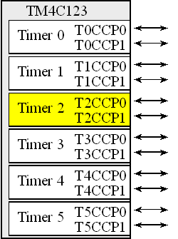
Figure T.3.1. Periodic timers on the TM4C123.
In periodic timer mode the timer is configured as a 32-bit down-counter, as shown in Figure T.3.2. When the timer counts from 1 to 0 it sets the trigger flag. On the next count, the timer is reloaded with the value in TIMER2_TAILR_R. We select periodic timer mode by setting the 2-bit TAMR field of the TIMER2_TAMR_R to 0x02. In periodic mode the timer runs continuously. The timers can be used to create pulse width modulated outputs and measure pulse width, period, or frequency.
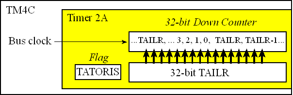
Figure T.3.2. Operation of Periodic Timer.
In this section we will use Timer2A to trigger a periodic interrupt. We will implement an abstraction, such that the low-level implementation is defined in Program T.3.1, and the high-level application is shown in Program T.3.2. As with all abstractions, we separate what it does (Program T.3.2) from how it works (Program T.3.1). The precision is 32 bits and the resolution will be the bus cycle time of 12.5 ns. This means we could trigger an interrupt as slow as every 232*12.5ns, which is 53 seconds. The interrupt period will be
(TIMER2_TAILR_R +1)*12.5ns
: If the bus clock is 80 MHz, what TAILR value do you need to interrupt at 1 Hz?
Each periodic timer module has
A clock enable bit, bit 2 in SYSCTL_RCGCTIMER_R
A control register, TIMER2_CTL_R (set to 0 to disable, 1 to enable)
A configuration register, TIMER2_CFG_R (set to 0 for 32-bit mode)
A mode register, TIMER2_TAMR_R (set to 2 for periodic mode)
A 32-bit reload register, TIMER2_TAILR_R
A resolution register, TIMER2_TAPR_R (set to 0 for 12.5ns)
An interrupt clear register, TIMER2_ICR_R (bit 0)
An interrupt arm bit, TATOIM, TIMER2_IM_R (bit 0)
A flag bit, TATORIS, TIMER2_RIS_R (bit 0)
void (*PeriodicTask2)(void); // user function
void Timer_Init(void(*task)(void), uint32_t period, uint32_t priority){
SYSCTL_RCGCTIMER_R |= 0x04; // 0) activate timer2
PeriodicTask2 = task; // user function
TIMER2_CTL_R = 0x00000000; // 1) disable timer2A during setup
TIMER2_CFG_R = 0x00000000; // 2) configure for 32-bit mode
TIMER2_TAMR_R = 0x00000002; // 3) configure for periodic mode, default down-count settings
TIMER2_TAILR_R = period-1; // 4) reload value
TIMER2_TAPR_R = 0; // 5) bus clock resolution
TIMER2_ICR_R = 0x00000001; // 6) clear timer2A timeout flag
TIMER2_IMR_R = 0x00000001; // 7) arm timeout interrupt
NVIC_PRI5_R = (NVIC_PRI5_R&0x00FFFFFF)|(priority<<29); // priority
// interrupts enabled in the main program after all devices initialized
// vector number 39, interrupt number 23
NVIC_EN0_R = 1<<23; // 9) enable IRQ 23 in NVIC
TIMER2_CTL_R = 0x00000001; // 10) enable timer2A
}
void Timer2A_Handler(void){
TIMER2_ICR_R = TIMER_ICR_TATOCINT; // acknowledge TIMER2A timeout
(*PeriodicTask2)(); // execute user task
}
void Timer_Stop(void){
NVIC_DIS0_R = 1<<23; // 9) disable interrupt 23 in NVIC
TIMER2_CTL_R = 0x00000000; // 10) disable timer2A
}
Program T.3.1. Periodic interrupts using Timer2A.
Observation: It is good design practice to disable interrupts at the start of main, perform all initialization, and then enable interrupts.
uint32_t Time; // time in msec
void MyTask(void){ // task to run at 1kHz
Debug_HeartBeat0(); // Program T.1.2
Time++;
}
#define F1000HZ (80000000/1000)
int main(void){
DisableInterrupts();
PLL_Init(Bus80MHz); // bus clock at 80 MHz
Debug_Init(); // initialize heartbeat
Time = 0;
Timer_Init(&MyTask, F1000HZ,2); // 1000 Hz
EnableInterrupts();
while(1){
Debug_HeartBeat1();
}
}
Program T.3.2. Use of periodic interrupts to maintain time in msec.
: Assume there is a scope connected to the heartbeat in MyTask. At what frequency will the heartbeat oscillate?
Video T.3.1. Timer2A
As shown in Figure T.3.1, there are six 32-bit timers on the TM4C123. Table T.3.1 shows the changes one must make to use the other timers.
| Register | Timer0 | Timer1 | Timer2 | Timer3 | Timer4 | Timer5 |
| SYSCTL_RCGCTIMER_R | bit 0 | bit 1 | bit 2 | bit 3 | bit 4 | bit 5 |
| Priority register | NVIC_PRI4_R | NVIC_PRI5_R | NVIC_PRI5_R | NVIC_PRI8_R | NVIC_PRI17_R | NVIC_PRI23_R |
| Priority bits | 31-29 | 15-13 | 31-29 | 31-29 | 23-21 | 7-5 |
| Enable register | NVIC_EN0_R | NVIC_EN0_R | NVIC_EN0_R | NVIC_EN1_R | NVIC_EN2_R | NVIC_EN2_R |
| Enable bit | 19 | 21 | 23 | 3 | 6 | 28 |
Table T.3.1. Changes to Program T.3.1 needed to use the six timers.
T.4.1. Registers
Next we will overview the specific UART functions on the TM4C microcontroller. Figure T.4.1 shows the UART protocol. The idle condition is high. The start bit is low. The data is transmitted one bit at a time b0 to b7. The frame ends in a stop bit, which is high. Because the idle and stop are high and the start is low, there is always a 1 to 0 transition at the start of a frame. The bit time is the width of each bit, the baud rate is 1/(bit time), and each frame is 10*(bit time). Since each frame contains one data byte, the bandwidth of the channel is 0.8*(baud rate).

Figure T.4.1. Full-duplex serial
communication channel.
TM4C microcontrollers have eight UARTs. The specific port pins used to implement the UARTs vary from one chip to the next. To find which pins your microcontroller uses, you will need to consult its datasheet. This section is intended to supplement rather than replace the Texas Instruments manuals. When designing systems with any I/O module, you must also refer to the reference manual of your specific microcontroller. It is also good design practice to review the errata for your microcontroller to see if any quirks (mistakes) exist in your microcontroller that might apply to the system you are designing. Table T.4.1 shows PCTL register for the TM4C123. Functionality U1Rx means UART1 reciever pin (input), and U1Tx means UART1 transmitter pin (output).
|
IO |
Ain |
0 |
1 |
2 |
3 |
4 |
5 |
6 |
7 |
8 |
9 |
14 |
|
PA0 |
|
Port |
U0Rx |
|
|
|
|
|
|
CAN1Rx |
|
|
|
PA1 |
|
Port |
U0Tx |
|
|
|
|
|
|
CAN1Tx |
|
|
|
PA2 |
|
Port |
|
SSI0Clk |
|
|
|
|
|
|
|
|
|
PA3 |
|
Port |
|
SSI0Fss |
|
|
|
|
|
|
|
|
|
PA4 |
|
Port |
|
SSI0Rx |
|
|
|
|
|
|
|
|
|
PA5 |
|
Port |
|
SSI0Tx |
|
|
|
|
|
|
|
|
|
PA6 |
|
Port |
|
|
I2C1SCL |
|
M1PWM2 |
|
|
|
|
|
|
PA7 |
|
Port |
|
|
I2C1SDA |
|
M1PWM3 |
|
|
|
|
|
|
PB0 |
|
Port |
U1Rx |
|
|
|
|
|
T2CCP0 |
|
|
|
|
PB1 |
|
Port |
U1Tx |
|
|
|
|
|
T2CCP1 |
|
|
|
|
PB2 |
|
Port |
|
|
I2C0SCL |
|
|
|
T3CCP0 |
|
|
|
|
PB3 |
|
Port |
|
|
I2C0SDA |
|
|
|
T3CCP1 |
|
|
|
|
PB4 |
Ain10 |
Port |
|
SSI2Clk |
|
M0PWM2 |
|
|
T1CCP0 |
CAN0Rx |
|
|
|
PB5 |
Ain11 |
Port |
|
SSI2Fss |
|
M0PWM3 |
|
|
T1CCP1 |
CAN0Tx |
|
|
|
PB6 |
|
Port |
|
SSI2Rx |
|
M0PWM0 |
|
|
T0CCP0 |
|
|
|
|
PB7 |
|
Port |
|
SSI2Tx |
|
M0PWM1 |
|
|
T0CCP1 |
|
|
|
|
PC4 |
C1- |
Port |
U4Rx |
U1Rx |
|
M0PWM6 |
|
IDX1 |
WT0CCP0 |
U1RTS |
|
|
|
PC5 |
C1+ |
Port |
U4Tx |
U1Tx |
|
M0PWM7 |
|
PhA1 |
WT0CCP1 |
U1CTS |
|
|
|
PC6 |
C0+ |
Port |
U3Rx |
|
|
|
|
PhB1 |
WT1CCP0 |
USB0epen |
|
|
|
PC7 |
C0- |
Port |
U3Tx |
|
|
|
|
|
WT1CCP1 |
USB0pflt |
|
|
|
PD0 |
Ain7 |
Port |
SSI3Clk |
SSI1Clk |
I2C3SCL |
M0PWM6 |
M1PWM0 |
|
WT2CCP0 |
|
|
|
|
PD1 |
Ain6 |
Port |
SSI3Fss |
SSI1Fss |
I2C3SDA |
M0PWM7 |
M1PWM1 |
|
WT2CCP1 |
|
|
|
|
PD2 |
Ain5 |
Port |
SSI3Rx |
SSI1Rx |
|
M0Fault0 |
|
|
WT3CCP0 |
USB0epen |
|
|
|
PD3 |
Ain4 |
Port |
SSI3Tx |
SSI1Tx |
|
|
|
IDX0 |
WT3CCP1 |
USB0pflt |
|
|
|
PD4 |
USB0DM |
Port |
U6Rx |
|
|
|
|
|
WT4CCP0 |
|
|
|
|
PD5 |
USB0DP |
Port |
U6Tx |
|
|
|
|
|
WT4CCP1 |
|
|
|
|
PD6 |
|
Port |
U2Rx |
|
|
M0Fault0 |
|
PhA0 |
WT5CCP0 |
|
|
|
|
PD7 |
|
Port |
U2Tx |
|
|
|
|
PhB0 |
WT5CCP1 |
NMI |
|
|
|
PE0 |
Ain3 |
Port |
U7Rx |
|
|
|
|
|
|
|
|
|
|
PE1 |
Ain2 |
Port |
U7Tx |
|
|
|
|
|
|
|
|
|
|
PE2 |
Ain1 |
Port |
|
|
|
|
|
|
|
|
|
|
|
PE3 |
Ain0 |
Port |
|
|
|
|
|
|
|
|
|
|
|
PE4 |
Ain9 |
Port |
U5Rx |
|
I2C2SCL |
M0PWM4 |
M1PWM2 |
|
|
CAN0Rx |
|
|
|
PE5 |
Ain8 |
Port |
U5Tx |
|
I2C2SDA |
M0PWM5 |
M1PWM3 |
|
|
CAN0Tx |
|
|
|
PF0 |
|
Port |
U1RTS |
SSI1Rx |
CAN0Rx |
|
M1PWM4 |
PhA0 |
T0CCP0 |
NMI |
C0o |
|
|
PF1 |
|
Port |
U1CTS |
SSI1Tx |
|
|
M1PWM5 |
PhB0 |
T0CCP1 |
|
C1o |
TRD1 |
|
PF2 |
|
Port |
|
SSI1Clk |
|
M0Fault0 |
M1PWM6 |
|
T1CCP0 |
|
|
TRD0 |
|
PF3 |
|
Port |
|
SSI1Fss |
CAN0Tx |
|
M1PWM7 |
|
T1CCP1 |
|
|
TRCLK |
|
PF4 |
|
Port |
|
|
|
|
M1Fault0 |
IDX0 |
T2CCP0 |
USB0epen |
|
|
Table T.4.1. PMCx bits in the GPIOPCTL register on the TM4C specify alternate functions. PD4 and PD5 are hardwired to the USB device. PA0 and PA1 are hardwired to the serial port.
: There are two choices for port pins to implement UART1. What are the choices?
: What port pins must we used to implement UART7?
: Why can't we use UART6 on the TM4C123 LaunchPad?
Table T.4.2 shows some of the registers for the UART1. For the other UARTs, the register names will replace the 1 with a 0-7. For the exact register addresses, you should include the appropriate header file (e.g., tm4c123gh6pm.h). To activate a UART you will need to turn on the UART clock in the RCGCUART register. You should also turn on the clock for the digital port in the RCGCGPIO register. You need to enable the transmit and receive pins as digital signals. The alternative function for these pins must also be selected. In particular we set bits in both the AFSEL and PCTL registers.
|
|
|
|
|
|
|
|
|
||
|
|
31-12 |
11 |
10 |
9 |
8 |
7-0 |
|
||
|
0x4000D000 |
|
OE |
BE |
PE |
FE |
DATA |
UART1_DR_R |
||
|
|
|
|
|
|
|
|
|
|
|
|
|
31-3 |
3 |
2 |
1 |
0 |
|
|||
|
0x4000D004 |
|
OE |
BE |
PE |
FE |
UART1_RSR_R |
|||
|
|
|
|
|
|
|
|
|
|
|
|
|
31-8 |
7 |
6 |
5 |
4 |
3 |
2-0 |
|
|
|
0x4000D018 |
|
TXFE |
RXFF |
TXFF |
RXFE |
BUSY |
|
UART1_FR_R |
|
|
|
|
|
|
|
|
|
|
|
|
|
|
31-16 |
15-0 |
|
||||||
|
0x4000D024 |
|
DIVINT |
UART1_IBRD_R |
||||||
|
|
|
|
|
|
|
|
|
|
|
|
|
31-6 |
5-0 |
|
||||||
|
0x4000D028 |
|
DIVFRAC |
UART1_FBRD_R |
||||||
|
|
|
|
|
|
|
|
|
|
|
|
|
31-8 |
7 |
6 - 5 |
4 |
3 |
2 |
1 |
0 |
|
|
0x4000D02C |
|
SPS |
WPEN |
FEN |
STP2 |
EPS |
PEN |
BRK |
UART1_LCRH_R |
|
|
|
|
|
|
|
|
|
|
|
|
|
31-10 |
9 |
8 |
7 |
6-3 |
2 |
1 |
0 |
|
|
0x4000D030 |
|
RXE |
TXE |
LBE |
|
SIRLP |
SIREN |
UARTEN |
UART1_CTL_R |
Table T.4.2. Some UART registers. Each register is 32 bits wide. Shaded bits are zero.
The OE, BE, PE, and FE are error flags associated with the receiver. You can see these flags in two places: associated with each data byte in UART1_DR_R or as a separate error register in UART1_RSR_R. The overrun error (OE) is set if data has been lost because the input driver latency is too long. BE is a break error, meaning the other device has sent a break. PE is a parity error (however, we will not be using parity). The framing error (FE) will get set if the baud rates do not match. The software can clear these four error flags by writing any value to UART1_RSR_R.
The status of the two FIFOs can be seen in the UART1_FR_R register. The BUSY flag is set while the transmitter still has unsent bits, even if the transmitter is disabled. It will become zero when the transmit FIFO is empty and the last stop bit has been sent. If you implement busy-wait output by first outputting then waiting for BUSY to become 0 (right flowchart of Figure T.4.2), then the routine will write new data and return after that particular data has been completely transmitted.
The UART1_CTL_R control register contains the bits that turn on the UART. TXE is the Transmitter Enable bit, and RXE is the Receiver Enable bit. We set TXE, RXE, and UARTEN equal to 1 in order to activate the UART device. However, we should clear UARTEN during the initialization sequence.
The IBRD and FBRD registers specify the baud rate. The baud rate divider is a 22-bit binary fixed-point value with a resolution of 2-6. The Baud16 clock is created from the system bus clock, with a frequency of (Bus clock frequency)/divider. The baud rate is 16 times slower than Baud16
Baud rate = Baud16/16 = (Bus clock frequency)/(16*divider)
For example, if the bus clock is 80 MHz and the desired baud rate is 19200 bits/sec, then the divider should be 80,000,000/16/19200 or 260.4167. Let m be the integer part, without rounding. We store the integer part (m=260) in IBRD. For the fraction, we find an integer n, such that n/64 is about 0.4167. More simply, we multiply 0.4167*64 = 26.6688 and round to the closest integer, 27. We store this fraction part (n=27) in FBRD. We did approximate the divider, so it is interesting to determine the actual baud rate. Assume the bus clock is 80 MHz.
Baud rate = (80 MHz)/(16* (m+n/64)) = (80 MHz)/(16* (260+27/64)) = 19199.616 bits/sec
The baud rates in the transmitter and receiver must match within 5% for the channel to operate properly. The error for this example is 0.002%.
The three registers LCRH, IBRD, and FBRD form an internal 30-bit register. This internal register is only updated when a write operation to LCRH is performed, so any changes to the baud-rate divisor must be followed by a write to the LCRH register for the changes to take effect. Out of reset, both FIFOs are disabled and act as 1-byte-deep holding registers. The FIFOs are enabled by setting the FEN bit in LCRH.
: Assume the bus clock is 80 MHz. What is the baud rate if UART1_IBRD_R equals 200 and UART1_FBRD_R equals 32?
: Assume the bus clock is 80 MHz. What values should you put in UART1_IBRD_R and UART1_FBRD_R to make a baud rate of 38400 bits/sec?
T.4.2. Busy-wait UART1 Device Driver on PC5 and PC4
Software that sends and receives data must implement a mechanism to synchronize the software with the hardware. In particular, the software should read data from the input device only when data is indeed ready. Similarly, software should write data to an output device only when the device is ready to accept new data. With busy-wait synchronization, the software continuously checks the hardware status waiting for it to be ready. In this section, we will use busy-wait synchronization to write I/O programs that send and receive data using the UART. After a frame is received, the receive FIFO will be not empty (RXFE becomes 0) and the 8-bit data is available to be read. To get new data from the serial port, the software first waits for RXFE to be zero, then reads the result from UART1_DR_R. Recall that when the software reads UART1_DR_R it gets data from the receive FIFO. This operation is illustrated in Figure T.4.2 and shown in Program T.4.1. In a similar fashion, when the software wishes to output via the serial port, it first waits for TXFF to be clear, then performs the output. When the software writes UART1_DR_R it puts data into the transmit FIFO.
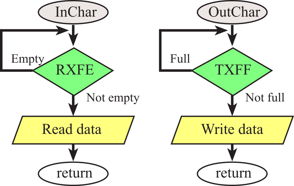
Figure T.4.2. Flowcharts of InChar and OutChar using busy-wait synchronization.
The initialization program, UART_Init, enables the UART1 device and selects the baud rate. The PCTL bits were defined back in Table T.4.1. PCTL bits 5-4 are set to 0x22 to select U1Tx and U1Rx on PC5 and PC4. The input routine waits in a loop until RXFE is 0 (FIFO not empty), then reads the data register. The output routine first waits in a loop until TXFF is 0 (FIFO not full), then writes data to the data register. Polling before writing data is an efficient way to perform output. There are UART examples in the starter code, busy-wait and interrupt-driven. Be careful when using Port C to be friendly; the pins PC3-PC0 are used by the debugger and you should not modify their configurations.
// Assumes a 80 MHz bus clock, creates 115200 baud rate
void UART_Init(void){ // should be called only once
SYSCTL_RCGCUART_R |= 0x00000002; // activate UART1
SYSCTL_RCGCGPIO_R |= 0x00000004; // activate port C
UART1_CTL_R &= ~0x00000001; // disable UART
UART1_IBRD_R = 43; // IBRD = int(80,000,000/(16*115,200)) = int(43.40278)
UART1_FBRD_R = 26; // FBRD = round(0.40278 * 64) = 26
UART1_LCRH_R = 0x00000070; // 8 bit, no parity bits, one stop, FIFOs
UART1_CTL_R |= 0x00000001; // enable UART
GPIO_PORTC_AFSEL_R |= 0x30; // enable alt funct on PC5-4
GPIO_PORTC_DEN_R |= 0x30; // configure PC5-4 as UART1
GPIO_PORTC_PCTL_R = (GPIO_PORTC_PCTL_R&0xFF00FFFF)+0x00220000;
GPIO_PORTC_AMSEL_R &= ~0x30; // disable analog on PC5-4
}
// Wait for new input, then return ASCII code
char UART_InChar(void){
while((UART1_FR_R&0x0010) != 0); // wait until RXFE is 0
return((char)(UART1_DR_R&0xFF));
}
// Wait for buffer to be not full, then output
void UART_OutChar(char data){
while((UART1_FR_R&0x0020) != 0); // wait until TXFF is 0
UART1_DR_R = data;
}
// Immediately return input or 0 if no input
char UART_InCharNonBlocking(void){
if((UART1_FR_R&UART_FR_RXFE) == 0){
return((char)(UART1_DR_R&0xFF));
} else{
return 0;
}
}
Program
T.4.1. Device driver functions that implement serial I/O.
Video T.4.1. UART Device Driver walk through
: How does the software clear RXFE?
: How does the software clear TXFF?
: Describe what happens if the receiving computer is operating on a baud rate that is twice as fast as the transmitting computer?
: Describe what happens if the transmitting computer is operating on a baud rate that is twice as fast as the receiving computer?
T.4.3. Interrupt UART1 Device Driver on PC5 and PC4
We use interrupt synchrononization when the system is complex and has many unrelated tasks to accomplish. Different from baud rate and format, the tranmitter and receiver do not need to use the same synchronization. For efficient performance, we will use busy-wait only when we know the software will never wait. For example, if the size of the tranmitted message is less than the size of the hardware TxFifo, and the rate of sending message allows the previous message to be completely sent before the next message is attempted, then busy-wait in the transmitter is allowed because it will never wait. Often this timing cannot be guaranteed, so interrupts are needed. To use interrupts we must enable the hardware FIFOs by setting the FEN bit in the UART1_LCRH_R register. RXIFLSEL specifies the receive FIFO level that causes an interrupt.
RXIFLSEL
Set RXRIS interrupt trigger when
0x0 ≥ 1/8 full Receive FIFO goes from 1
to 2 characters
0x1 ≥ 1/4 full Receive FIFO goes from 3
to 4 characters
0x2 ≥ 1/2 full Receive FIFO goes from 7 to 8
characters
0x3 ≥ 3/4 full Receive FIFO goes from 11
to 12 characters
0x4 ≥ 7/8 full Receive FIFO goes from 13
to 14 characters
TXIFLSEL specifies the transmit FIFO level that causes an
interrupt.
TXIFLSEL
Set TXRIS
interrupt trigger when
0x0 ≤ 7/8 empty Transmit FIFO goes from 15 to 14
characters
0x1 ≤ 3/4 empty Transmit FIFO goes from 13 to 12
characters
0x2 ≤ 1/2 empty Transmit FIFO goes from 9 to 8
characters
0x3 ≤ 1/4 empty Transmit FIFO goes from 5 to 4 characters
0x4 ≤ 1/8 empty Transmit FIFO goes from 3 to 2 characters
The register UART1_IM_R contains the ARM
bits.
Bit 6 RTIM arm receiver timeout
Bit 5 TXIM arm transmit FIFO (see TXIFLSEL)
Bit 4 RXIM arm receive FIFO (see RXIFLSEL)
The register UART1_RIS_R contains the trigger flag (set by
hardware on UART event).
Bit 6 RTRIS trigger flag for receiver timeout
Bit 5 TXRIS trigger flag for transmit FIFO (see
TXIFLSEL)
Bit 4 RXRIS trigger flag for receive FIFO (see
RXIFLSEL)
The register UART1_ICR_R contains the acknowledge bits
(software writes 1 to clear trigger flag).
Bit 6 RTIC acknowledge receiver timeout
Bit 5 TXIC acknowledge transmit FIFO (see TXIFLSEL)
Bit 4 RXIC acknowledge receive FIFO (see RXIFLSEL)
Figure T.4.3 shows a data flow graph with buffered input and buffered output. FIFOs used in this book will be statically allocated global structures. Because they are global variables, it means they will exist permanently and can be carefully shared by more than one program. The advantage of using a FIFO structure for a data flow problem is that we can decouple the producer and consumer threads. Without the FIFO we would have to produce one piece of data, then process it, produce another piece of data, then process it. With the FIFO, the producer thread can continue to produce data without having to wait for the consumer to finish processing the previous data. This decoupling can significantly improve system performance.
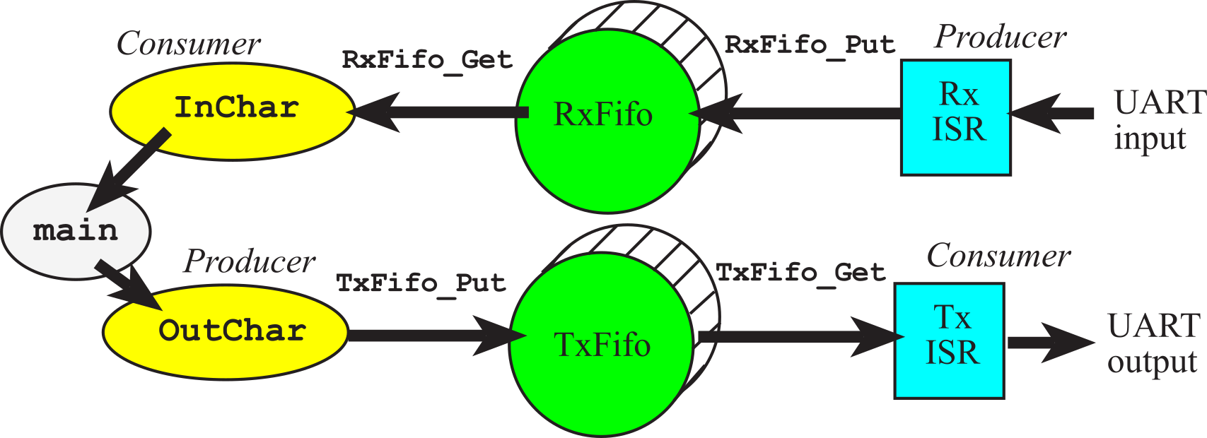
Figure T.4.2. A data flow graph showing two FIFOs that buffer data between producers and consumers.
The flowchart for using two FIFOs is illustrated in Figure T.4.4. With mailbox synchronization, the threads execute in lock-step: one, the other, one, the other… However, with the FIFO queue execution of the threads is more loosely coupled. The classic producer/consumer problem has two threads. One thread produces data and the other consumes data. For an input device, the background thread is the producer because it generates new data, and the foreground thread is the consumer because it uses the data up. For an output device, the data flows in the other direction so the producer/consumer roles are reversed. It is appropriate to pass data from the producer thread to the consumer thread using a FIFO queue
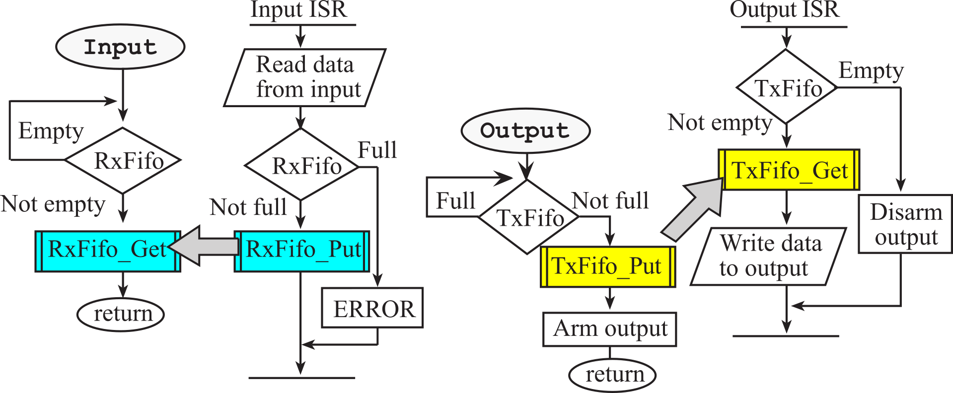
Figure T.4.4. In a producer/consumer system, FIFO queues can be used to pass data between threads.
Details of the NVIC interrupts can be found back in Section 6.3 of the ECE319K ebook. Refer to Section 6.3 to answer these next three
checkpoints:
: At what address is the UART1_Handler ISR vector?
: How do you arm UART1_Handler ISR in the NVIC?
: Where are the priority bits for the UART1 interrupt 6?
Figure T.4.5 shows a data flow graph of two microcontrollers connected with UART. Because the signals are encoded as voltages, the grounds must connected together. Figure T.4.5 is classified as full-duplex, because transmission can occur in both directions simultaneously.
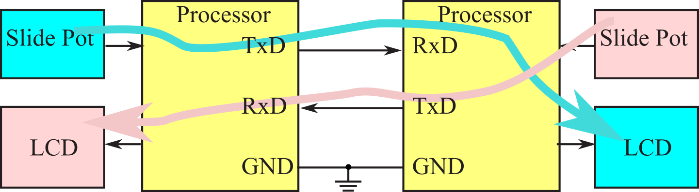
Figure T.4.5. Full-duplex serial
communication channel.
#define FIFOSIZE 16 // size of the FIFOs (must be power of 2)
#define FIFOSUCCESS 1 // return value on success
#define FIFOFAIL 0 // return value on failure
AddIndexFifo(Rx, FIFOSIZE, char, FIFOSUCCESS, FIFOFAIL)
AddIndexFifo(Tx, FIFOSIZE, char, FIFOSUCCESS, FIFOFAIL)
// Assumes an 80 MHz bus clock
void UART_Init(uint32_t baud, uint32_t priority){ // should be called only once
SYSCTL_RCGCUART_R |= 0x0002; // activate UART1
SYSCTL_RCGCGPIO_R |= 0x0004; // activate port C
RxFifo_Init(); // initialize software FIFOs
TxFifo_Init();
UART1_CTL_R &= ~0x01; // disable UART
UART1_IBRD_R = 5000000/baud; // IBRD = int(80,000,000 / (16 * baud))
UART1_FBRD_R = ((64*(5000000%baud))+baud/2)/baud; // FBRD = round(remainder * 64 + 0.5)
UART1_LCRH_R = 0x0070; // 8-bit word length, enable FIFO
UART1_IFLS_R &= ~0x3F; // set TX and RX interrupt FIFO level fields
// configure interrupt for TX FIFO <= 1/8 full
// configure interrupt for RX FIFO >= 1/8 full
UART1_IM_R |= 0x70;// enable TX and RX FIFO interrupts and RX time-out interrupt
UART1_CTL_R |= 0x0301; // enable RXE TXE UARTEN
GPIO_PORTC_PCTL_R = (GPIO_PORTC_PCTL_R&0xFF00FF00)+0x00220000; // UART1
GPIO_PORTC_AMSEL_R &= ~0x30; // disable analog on PC5-4
GPIO_PORTC_AFSEL_R |= 0x30; // enable alt funct on PC5-4
GPIO_PORTC_DEN_R |= 0x30; // enable digital I/O on PC5-4
NVIC_PRI1_R = (NVIC_PRI1_R&0xFF00FFFF)|(priority<<21); // UART1=priority 2
NVIC_EN0_R = 1<<6; // enable interrupt 6 in NVIC
EnableInterrupts();
}
// copy from hardware RX FIFO to software RX FIFO
// stop when hardware RX FIFO is empty or software RX FIFO is full
void static copyHardwareToSoftware(void){ char letter;
while(((UART1_FR_R&0x10)==0)&&(RxFifo_Size() < (FIFOSIZE-1))){
letter = UART1_DR_R;
RxFifo_Put(letter);
}
}
// copy from software TX FIFO to hardware TX FIFO
// stop when software TX FIFO is empty or hardware TX FIFO is full
void static copySoftwareToHardware(void){ char letter;
while(((UART1_FR_R&0x20) == 0) && (TxFifo_Size() > 0)){
TxFifo_Get(&letter);
UART1_DR_R = letter;
}
}
// input ASCII character from UART
// spin if RxFifo is empty
char UART_InChar(void){
char letter;
while(RxFifo_Get(&letter) == FIFOFAIL){}; // spin if no data
return(letter);
}
// output ASCII character to UART
// spin if TxFifo is full
void UART_OutChar(char data){
while(TxFifo_Put(data) == FIFOFAIL){}; // spin if TxFIFO has no room
UART1_IM_R &= ~0x20; // disable TX FIFO interrupt
copySoftwareToHardware();
UART1_IM_R |= 0x20; // enable TX FIFO interrupt
}
// at least one of three things has happened:
// hardware TX FIFO goes from 3 to 2 or less items
// hardware RX FIFO goes from 1 to 2 or more items
// UART receiver has timed out with one or more items available
void UART1_Handler(void){
if(UART1_RIS_R&0x20){ // hardware TX FIFO <= 2 items
UART1_ICR_R = 0x20; // acknowledge TX FIFO
// copy from software TX FIFO to hardware TX FIFO
copySoftwareToHardware();
if(TxFifo_Size() == 0){ // software TX FIFO is empty
UART1_IM_R &= ~0x20; // disable TX FIFO interrupt
}
}
if(UART1_RIS_R&0x10){ // hardware RX FIFO >= 2 items
UART1_ICR_R = 0x10; // acknowledge RX FIFO
// copy from hardware RX FIFO to software RX FIFO
copyHardwareToSoftware();
}
if(UART1_RIS_R&0x40){ // receiver timed out
UART1_ICR_R = 0x40; // acknowledge receiver time out
// copy from hardware RX FIFO to software RX FIFO
copyHardwareToSoftware();
}
}
Program T.4.2. Interrupt-driven device driver for the UART uses two hardware FIFOs and two software FIFOs to buffer data.
As shown in Figure T.4.1, there are eight UARTs
on the TM4C123. Table T.4.3 shows the changes one must make to use the other
UARTs. UART6 is not included because it cannot be used on the LaunchPad.
| Register | UART0 | UART1 | UART2 | UART3 | UART4 | UART5 | UART7 |
| SYSCTL_RCGCUART_R | bit 0 | bit 1 | bit 2 | bit 3 | bit 4 | bit 5 | bit 7 |
| Priority register | NVIC_PRI1_R | NVIC_PRI1_R | NVIC_PRI8_R | NVIC_PRI14_R | NVIC_PRI15_R | NVIC_PRI15_R | NVIC_PRI15_R |
| Priority bits | 15-13 | 23-21 | 15-13 | 31-29 | 7-5 | 15-13 | 23-21 |
| Enable register | NVIC_EN0_R | NVIC_EN0_R | NVIC_EN1_R | NVIC_EN1_R | NVIC_EN1_R | NVIC_EN1_R | NVIC_EN1_R |
| Enable bit | 5 | 6 | 1 | 27 | 28 | 29 | 30 |
Table T.4.3. Changes to Program T.4.2 needed to use the other UARTs.
T.5. Synchronous Transmission and Receiving using the SSI
T.5.1. Details on the TM4C123
Texas Instruments defines all its synchronous protocols synchronous serial interface (SSI), which includes SPI. The SSI protocol includes four I/O lines. The slave select SSI0Fss is an optional negative logic control signal from master to slave signal signifying the channel is active. The second line, SCK, is a 50% duty cycle clock generated by the master. The SSI0Tx (master out slave in, MOSI) is a data line driven by the master and received by the slave. The SSI0Rx (master in slave out, MISO) is a data line driven by the slave and received by the master. To work properly, the transmitting device uses one edge of the clock to change its output, and the receiving device uses the other edge to accept the data. Table T.4.1 shows the PCTL values needed to specify I/O pins as SSI modules on the TM4C123.
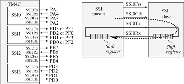
Figure T.5.1. Synchronous serial port pins on the TM4C123 microcontroller.
On the TM4C the shift register can be configured from 4 to 16 bits. The shift register in the master and the shift register in the slave are linked to form a distributed register. Figure T.5.2 illustrates communication between master and slave. Typically, the microcontroller and the I/O device slave are so physically close we do not use interface logic.
The SSI on the TM4C employs two hardware FIFOs. Both FIFOs are 8 elements deep and 4 to 16 bits wide, depending on the selected data width. When performing I/O the software puts into the transmit FIFO by writing to the SSI0_DR_R register and gets from the receive FIFO by reading from the SSI0_DR_R register.
If there is data in the transmit FIFO, the SSI module will transmit it. With SSI it transmits and receives bits at the same time. When a data transfer operation is performed, this distributed 8- to 32-bit register is serially shifted 4 to 16 bit positions by the SCK clock from the master so the data is effectively exchanged between the master and the slave. Data in the master shift register are transmitted to the slave. Data in the slave shift register are transmitted to the master.
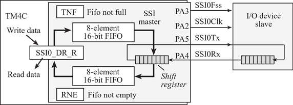
Figure T.5.2. A synchronous serial interface between a microcontroller and an I/O device.
Table T.5.1 lists the SSI0 registers on the TM4C. The TM4C can operate in slave mode, but we will focus on master mode. The PCTL bits are defined in Table T.4.1 .
|
Address |
31-6 |
3 |
2 |
1 |
0 |
Name |
||||||||||
|
0x400FE61C |
|
SSI3 |
SSI2 |
SSI1 |
SSI0 |
SYSCTL_RCGCSSI_R |
||||||||||
|
|
|
|
|
|
|
|
|
|
|
|||||||
|
|
31-16 |
15-8 |
7 |
6 |
5-4 |
3-0 |
|
|||||||||
|
0x40008000 |
|
SCR |
SPH |
SPO |
FRF |
DSS |
SSI0_CR0_R |
|||||||||
|
|
|
|
|
|
|
|
|
|
|
|||||||
|
|
31-16 |
15-0 |
|
|||||||||||||
|
0x40008008 |
|
Data |
SSI0_DR_R |
|||||||||||||
|
|
|
|
|
|
|
|
|
|
|
|||||||
|
|
7 |
6 |
5 |
4 |
3 |
2 |
1 |
0 |
|
|||||||
|
0x40008004 |
|
|
|
|
SOD |
MS |
SSE |
LBM |
SSI0_CR1_R |
|||||||
|
0x4000800C |
|
|
|
BSY |
RFF |
RNE |
TNF |
TFE |
SSI0_SR_R |
|||||||
|
0x40008010 |
CPSDVSR |
SSI0_CPSR_R |
||||||||||||||
|
0x40008014 |
|
|
|
|
TXIM |
RXIM |
RTIM |
RORIM |
SSI0_IM_R |
|||||||
|
0x40008018 |
|
|
|
|
TXRIS |
RXRIS |
RTRIS |
RORRIS |
SSI0_RIS_R |
|||||||
|
0x4000801C |
|
|
|
|
TXMIS |
RXMIS |
RTMIS |
RORMIS |
SSI0_MIS_R |
|||||||
|
0x40008020 |
|
|
|
|
|
|
RTIC |
RORIC |
SSI0_ICR_R |
|||||||
|
0x40058420 |
SEL |
SEL |
SEL |
SEL |
SEL |
SEL |
SEL |
SEL |
GPIO_PORTA_AFSEL_R |
|||||||
|
0x4005841C |
DEN |
DEN |
DEN |
DEN |
DEN |
DEN |
DEN |
DEN |
GPIO_PORTA_DEN_R |
|||||||
|
0x40058400 |
DIR |
DIR |
DIR |
DIR |
DIR |
DIR |
DIR |
DIR |
GPIO_PORTA_DIR_R |
|||||||
|
0x400FE608 |
GPIOH |
GPIOG |
GPIOF |
GPIOE |
GPIOD |
GPIOC |
GPIOB |
GPIOA |
SYSCTL_RCGCGPIO_R |
|||||||
Table T.5.1. The TM4C SSI0 registers. Each register is 32 bits wide. Bits 31 - 8 are zero.
The SSI clock frequency is established by the 8-bit field SCR field in the SSI0_CR0_R register and the 8-bit field CPSDVSR field in the SSI0_CPSR_R register. SCR can be any 8‑bit value from 0 to 255. CPSDVSR must be an even number from 2 to 254. Let fBUS be the frequency of the bus clock. The frequency of the SSI is
fSSI = fBUS / (CPSDVSR * (1 + SCR))
Common control features for the SSI
module include:
- Baud rate control register, used to select the transmission rate
- Data size 4 to 16 bits, set 4-bit DSS field equal to size-1
- Mode bits in the control register to select
- Master versus slave
- Freescale mode with clock polarity and clock phase
- Other modes like TI synchronous or Microwire mode
- Interrupt arm bit
- Ability to make the outputs open drain (open collector)
Common status bits for the SPI
module include:
- BSY, SSI is currently transmitting and/or receiving a frame
- RFF, SSI receive FIFO is full
- RNE, SSI receive FIFO is not empty
- TNF, SSI transmit FIFO is not full
- TFE, SSI transmit FIFO is empty
The key to proper transmission is to select one edge of the clock (shown as "T" in Figure T.5.3) to be used by the transmitter to change the output, and use the other edge (shown as "R") to latch the data in the receiver. In this way data is latched during the time when it is stable. Data available is the time when the output data is actually valid, and data required is the time when the input data must be valid.
During transmission, the output data will be valid from S5max after the clock edge until S5min after the next clock edge. The maximum S5 time is 1 system bus period (e.g., 20ns) and the minimum is 0. When receiving the setup time (S8) is 1 system bus period and the hold time (S9) is 2 system bus periods. For the communication to occur without error, the data available from the device that is driving the data line must overlap (start before and end after) the data required by the other device that is receiving the data. It is this overlap that will determine the maximum frequency at which synchronous serial communication can occur. Remember to add the propagation delay in cable.
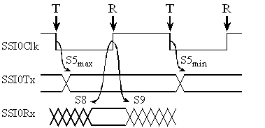
Figure T.5.3. Synchronous serial timing showing data available on MOSI and data required on MISO for the TM4C123.
: What are the definitions of setup time and hold time?
Observation: When transmitting multiple frames, the Fss signal goes low and high for each frame. If you need Fss to fall and rise once, you'll have to program it as a GPIO as make it fall and rise in software.
The Freescale SPI timing is shown in Figure T.5.4 (FRF=00).
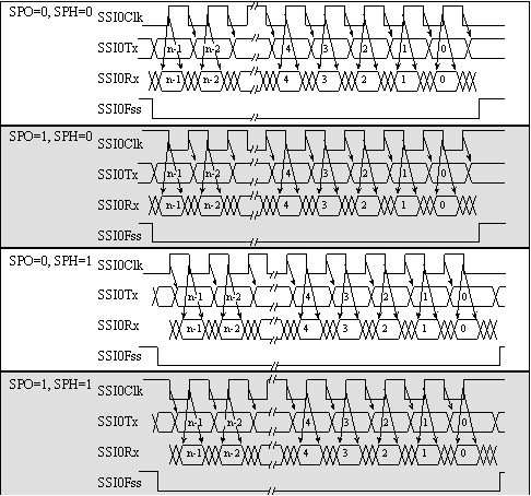
Figure T.5.4. Synchronous serial Freescale single transfer mode (n is 4 to 16 bits).
The SPI transmits data at the same time as it receives input. In the Freescale modes, the SPI changes its output on the opposite edge of the clock as it uses to shift data in. There are three mode control bits (MS, SPO, SPH) that affect the transmission protocol. If the device is a master (MS=0) it generates the SCLK, and data is output on the SSI0Tx pin, and input on the SSI0Rx pin. The SPO control bit specifies the polarity of the SCLK. In particular, the SPO bit specifies the logic level of the clock when data is not being transferred. The SPH bit affects the timing of the first bit transferred and received. If SPH is 0, then the device will shift data in on the first (and 3rd, 5th, 7th, ... etc.) clock edge. If SPH is 1, then the device will shift data in on the second (and 4th, 6th, 8th, ... etc.) clock edge. The data is transmitted MSB first.
The TM4C123 also supports TI synchronous (FRF=01, Figure T.5.5) and Microwire (FRF=10) modes. Refer to the data sheets for details of these modes.
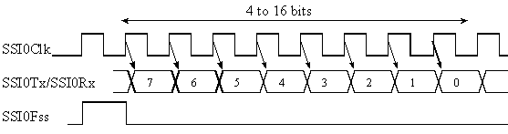
Figure T.5.5. Synchronous serial TI single transfer mode.
T.5.2. MAX5353 DAC example
This example shows a synchronous serial interface between the microcontroller and a Maxim MAX5353 12-bit digital to analog converter as drawn in Figure T.5.6. A digital to analog converter (DAC) accepts a digital input (in our case a number between 0 and 4095) and creates an analog output (in our case a voltage between 0 and VREF*GAIN.) Discussion of DACs is presented in Section 5.2. Here in this section, we will focus on the digital hardware and software aspects of the serial interface.
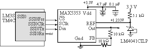
Figure T.5.6. A 12-bit DAC interfaced to the SSI port.
Table T.5.2 and Figure T.5.7 describe the protocol. The first 3 bits sent will be zero, then the 12 data bits that specify the analog output, and then one more zero will be sent. The SSI0Fss control signal will be low during the 16-bit transmission. As with any SPI interface, there are basic interfacing issues to consider.
Word size. In this case we need to transmit 16 bits to the DAC. The MAX5353 data sheet specifies that the first three bits are command codes, the next 12 bits are the DAC output (MSB transmitted first), and the last bit is zero. Bit order. The MAX5353 requires the most significant bits first.
Clock phase, clock polarity. There are two issues to resolve. Since the MAX5353 samples its serial input data on the rising edge of the clock, the SSI must change the data on the falling edge. SPO=SPH=0 (Figure 7.17) and SPO=SPH=1 both satisfy this requirement. The second issue is which edge comes first the rise or the fall. In this interface it probably doesn't matter.
Bandwidth. We look at the timing specifications of the MAX5353. The minimum clock low width of 40 ns means the shortest SSI period we can use is 100 ns. The commands are:
|
C2 |
C1 |
C0 |
D11 : D0 MSB LSB |
S0 |
Description |
|
X |
0 |
0 |
12 bits of data |
0 |
Load input register; DAC register immediately updated. |
|
X |
0 |
1 |
12 bits of data |
0 |
Load input register; DAC register unchanged. |
|
X |
1 |
0 |
XXXXXXXXXXXX |
X |
Update DAC register from input register. |
|
1 |
1 |
1 |
XXXXXXXXXXXX |
X |
Shutdown |
|
0 |
1 |
1 |
XXXXXXXXXXXX |
X |
No operation |
Table T.5.2. MAX5353 protocols
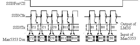
Figure T.5.7. MAX5353 DAC serial timing.
The ritual initializes the Freescale SPI master mode, 16-bit data, and 8 MHz bandwidth. To change the DAC output, one 16-bit transmission is sent (DAC_Out). The data returned in this case is not significant because the DAC does not return data, so the SSI0Rx pin in Figure T.5.6 is left not connected. In this example, the bus clock is 16 MHz, and the SPI clock will be 8 MHz.
void DAC_Init(uint16_t data){
SYSCTL_RCGCSSI_R |= 0x01; // activate SSI0
SYSCTL_RCGCGPIO_R |= 0x01; // activate port A
while((SYSCTL_PRGPIO_R&0x01) == 0){};// ready?
GPIO_PORTA_AFSEL_R |= 0x2C; // enable alt funct on PA2,3,5
GPIO_PORTA_DEN_R |= 0x2C; // configure PA2,3,5 as SSI
GPIO_PORTA_PCTL_R = (GPIO_PORTA_PCTL_R&0xFF0F00FF)+0x00202200;
GPIO_PORTA_AMSEL_R = 0; // disable analog functionality on PA
SSI0_CR1_R = 0x00000000; // disable SSI, master mode
SSI0_CPSR_R = 0x02; // 8 MHz SSIClk
SSI0_CR0_R &= ~(0x0000FFF0); // SCR = 0, SPH = 0, SPO = 0 Freescale
SSI0_CR0_R |= 0x0F; // DSS = 16-bit data
SSI0_DR_R = data; // load 'data' into transmit FIFO
SSI0_CR1_R |= 0x00000002; // enable SSI
}
void DAC_Out(uint16_t code){
while((SSI0_SR_R&0x00000002)==0){};// SSI Transmit FIFO Not Full
SSI0_DR_R =
code; // data out, no reply
}
Program T.5.1. Functions to initialize and to send data to the MAX5353 DAC using the SPI.
: How would you change Program T.5.2 to run at 10 MHz, assuming the bus frequency is 80 MHz?
T.5.3. ADXL362 accelerometer example
This second SSI example shows a synchronous serial interface between the computer and an ADXL362 3-axis MEMS Accelerometer, which measures acceleration in three dimensions. Here in this section we will focus on the hardware and software aspects of the serial interface (Figure T.5.8). Again, the basic interfacing issues to consider for this interface are:
Word size. Two write a command we need to transmit 24 bits to the ADXL362. To read a result, we first transmit 16 bits and then we receive 8 bits. The software will implement 8-bit transmissions with the SPI module.
Bit order. The ADXL362 requires the most significant bits first.
Clock phase, clock polarity. Since the ADXL362 samples its serial input data on the rising edge of the clock, the SPI must changes the data on the falling edge. SPO=SPH=0 and SPO=SPH=1 both satisfy this requirement. We will use the SPO=SPH=0 mode as suggested in the Analog Devices data sheet, refer back to Figure T.5.4.
Bandwidth. We look at the timing specifications of the ADXL362. The maximum SCLK frequency is 8 MHz, and the minimum clock low/high widths is 50 ns, so the shortest SPI period we can use is 125ns.
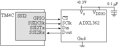
Figure T.5.8. A three-axis accelerometer interfaced to the SSI port.
The first 8 bits sent will specify read (0x0B) or write (0x0A) as shown in Figure T.5.9. The second 8 bits will specify the register from which to read, or to which to write. On a read operation the last 8 bits will be the value returned from the ADXL362 to the microcontroller. On a write operation, the last 8 bits will be the value written from the microcontroller to the ADXL362. Because we want the CS signal to remain low for the entire 24-bit transfer, we will implement it using the regular I/O pin functions.
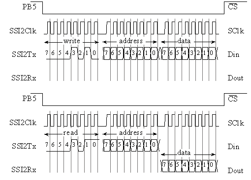
Figure T.5.9. ADXL362 serial timing.
Recall that when the software outputs to the SSI data register, the 8-bit register in the SSI is exchanged with the 8-bit register in the ADXL362. To communicate with the ADXL362, three 8-bit transmissions are exchanged.
#define PB5 (*((volatile uint32_t *) 0x40005080))
void ADXL362_Init(void){
SYSCTL_RCGCSSI_R |= 0x04; // activate SSI2
SYSCTL_RCGCGPIO_R |= 0x02; // activate port B
while((SYSCTL_PRGPIO_R&0x02) == 0){};// ready?
GPIO_PORTB_PCTL_R = (GPIO_PORTB_PCTL_R&0x00F0FFFF)+0x22020000;
GPIO_PORTB_AMSEL_R = 0; // disable analog functionality on PA
GPIO_PORTB_AFSEL_R |= 0xD); // enable alt funct on PB4,6,7
GPIO_PORTB_DIR_R |= 0x20; // make PB5 out (!CS signal)
GPIO_PORTB_DEN_R |= 0xF0; // enable digital I/O on PB4,5,6,7
PB5 = 0x20; // !CS = 1
SSI2_CR1_R = 0x00000000; // disable SSI, master mode
SSI2_CPSR_R = 0x08; // 2 MHz SSIClk (16MHz/8)
SSI2_CR0_R &= ~(0x0000FFF0); // clear SCR, SPH and SPO
SSI2_CR0_R |= 0x07; // DSS = 8-bit data
SSI2_CR1_R |= 0x00000002; // enable SSI
}
// send the 8-bit code, wait for reply, return reply
// basically this eliminates the FIFO, doing one at a time
uint8_t sendAfterWaiting(uint8_t code){uint8_t dummy;
while(SSI2_SR_R&SSI_SR_RNE){ // optional step
dummy = SSI2_DR_R; // flush any leftover bytes in receiver
}
while((SSI2_SR_R&SSI_SR_TFE)==0){};// wait until FIFO empty
SSI2_DR_R = code; // data out
while((SSI2_SR_R&SSI_SR_RNE)==0){};// wait until response
return SSI2_DR_R; // acknowledge response
}
void ADXL362_Write(uint8_t reg , uint8_t data){
PB5 = 0; // !CS = 0
sendAfterWaiting(0x0A); // send write operation
sendAfterWaiting(reg); // send register address
sendAfterWaiting(data); // write value
PB5 = 0x20; // !CS = 1
}
uint8_t ADXL362_Read(uint8_t reg){ uint8_t data;
PB5 = 0; // !CS = 0
sendAfterWaiting(0x0B); // send read operation
sendAfterWaiting(reg); // send register address
data = sendAfterWaiting(0); // read value
PB5 = 0x20; // !CS = 1
return data; // right justify
}
Program T.5.2. Functions to initialize, to send and to receive data from the ADXL362 using the SPI.
: How would you change Program T.5.2 to run at 2 MHz, assuming the bus frequency is 80 MHz?
T.5.4. Parallel port expander example
Sometimes we need more output pins than available on our microcontroller. In general, the proper design approach would be to upgrade to a microcontroller with more pins. However, in situations where we do not have the time or money to change microcontrollers, we can interface a 74HC595 shift register to the SSI port for a quick solution providing additional output pins. Basically, three pins of the SSI (SS, MOSI, and SCLK) will be converted to eight digital outputs Q on the 74HC595, as shown in Figure T.5.10.
Additional shift registers can be chained together (connect the QH' outputs of one to the SER inputs of the next) to provide additional outputs without requiring more TM4C123 pins. The gate input, G*, of the 74HC595 is grounded so the eight Q outputs will be continuously driven. The SPI clock output is connected to the 74HC595 clock input (SCK) and the SPI data output is connected to the 74HC595 data input (SER). The Freescale SPI mode (SPO=0, SPH=0) is selected to the TM4C123 changes the output data on the fall of the clock and the 74HC595 shifts data in on the rise. Because the 74HC595 is fast (maximum clock 25 MHz, and setup time of 20 ns), we run the SSI as fast as possible. If the bus clock is 16 MHz and the divider is set to 2, and the SSI clock will be 8 MHz.
After eight bits are transferred from the TM4C123 to the 74HC595, software will create a rising edge of RCK, causing the new data to be latched into the 74HC595. If there is just one 74HC595 like Figure T.5.10, we can use the automatic Fss feature of the SPI to create a rising edge latch on RCLK. To enable SPI, we set bits 2,3,5 AFSEL for Port A. The PCTL code for SSI on Port A is 2 (Table T.4.1). In this solution, we perform one SSI transmission to change all 8 bits of the port output (Program T.5.3). The Fss pulse occurs automatically and does not require software overhead to produce. However, if we were chaining multiple shift registers, we would not use the automatic Fss feature; rather we would output all the data and then manually latch them all in with explicit outputs on RCK by using PA3 as a regular GPIO port.
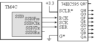
Figure T.5.10. Interface between the TM4C123 and a 74HC595 shift register.
Program T.5.3 assumes the system clock rate is 80 MHz. The clock divider is 10 so that the SPI clock will be 8 MHz, taking about 1 μs to output 8 bits to the port.
void Port_Init(void){
SYSCTL_RCGCSSI_R |= 0x01; // activate SSI0
SYSCTL_RCGCGPIO_R |= 0x01; // activate port A
while((SYSCTL_PRGPIO_R&0x01) == 0){};// ready?
GPIO_PORTA_AFSEL_R |= 0x2C; // enable alt funct on PA2,3,5
GPIO_PORTA_PCTL_R = (GPIO_PORTA_PCTL_R&0xFF0F00FF)+0x00202200;
GPIO_PORTA_AMSEL_R = 0; // disable analog functionality on PA
GPIO_PORTA_DEN_R |= 0x2C; // enable digital I/O on PA2,3,5
SSI0_CR1_R = 0x00000000; // disable SSI, master mode
SSI0_CPSR_R = 10; // 80MHz/10= 8 MHz SSIClk
SSI0_CR0_R &= ~(0x0000FFF0); // SCR = 0, SPH = 0, SPO = 0 Freescale
SSI0_CR0_R = (SSI0_CR0_R&~0x0F)+0x07; // 8-bit d ata
SSI0_CR1_R |= 0x00000002; // enable SSI
}
void Port_Out(uint8_t code){
while((SSI0_SR_R&0x02)==0){}; // wait until room in FIFO
SSI0_DR_R = code; // data out
}
Program T.5.3. Software to control an output parallel port expanded using the SSI.
: How would you change Program T.5.3 to run at 20 MHz, assuming the bus frequency is 80 MHz?
T.5.5. ST7735R LCD example
The ST7735R uses SPI protocol, see Figure T.5.11. The software writes into the SSI_DR_R data register, data passes through an 8-element hardware FIFO, and then each 8-bit byte is sent in serial fashion to the display. MOSI stands for master out slave in; the interface will send information one bit at a time over this line. SCK is the serial clock used to synchronize the shift register in the TM4C123 and the shift register in the ST7735R. TFT_CS is the chip select for the display; the interface will automatically make this signal low (active) during communication. D/C stands for data/command; software will make D/C high to send data and low to send a command.
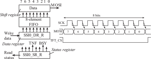
Figure T.5.11. Block diagram and SPI timing for the ST7735R.
Because the transfer of one byte of data only requires 1μs to complete, we will use "busy-wait" synchronization implemented in Program T.5.4. The software issues an output command to the LCD, it will wait until the display is not busy. In particular, the software will wait for the previous LCD command to be completed. Writing an 8-bit command requires 4 steps. Step 1) wait for the BUSY bit to be low. Step 2) Clear D/C=PA6 to zero (configured for COMMAND). Step 3) Write the command to SSI0_DR_R. Step 4) wait for the BUSY bit to be low. The two busy-wait steps guarantee the command is completed before the software function returns. Writing an 8-bit data value also uses busy-wait synchronization. Writing an 8-bit data value requires 3 steps. Step 1) wait for the transmit FIFO to have space. Step 2) Set D/C=PA6 to one (configured for DATA). Step 3) Write the data to SSI0_DR_R. The busy-wait step on "FIFO not full" means software can stream up to 8 data bytes without waiting for each data to complete.
void static writecommand(uint8_t command){
while((SSI0_SR_R&0x10)== 0x10){}; // wait until SSI0 not busy
GPIO_PORTA_DATA_R &= ~0x40; // PA6=0 means command
SSI0_DR_R = command; // command written to LCD
while((SSI0_SR_R&0x10)== 0x10){}; // wait until SSI0 not busy
}
void static writedata(uint8_t data){
while((SSI0_SR_R&0x02)==0){}; // wait for transmit FIFO not full
GPIO_PORTA_DATA_R |= 0x40; // PA6=1 means data
SSI0_DR_R = data; // data written to LCD
}
Program T.5.4. Low-level functions to output data/commands to the LCD display.
There is a rich set of graphics functions available for the ST7735R, allowing you to create amplitude versus time, or bit-mapped graphics. Refer to the ST7735R.h header file for more details.
T.6. TM4C I2C Details
TM4C microcontrollers have zero to ten I2C modules, see Figure T.6.1. As shown in Figure T.6.1, microcontroller pins SDA and SCL can be connected directly to an I2C network. Because I2C networks are intended to connect devices on the same PCB, no special hardware interface electronics are required.
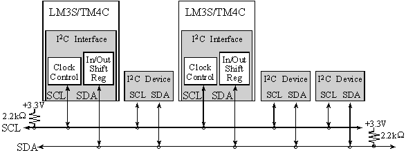
Figure T.6.1. Block diagram of an I2C communication network Use 1kΩ resistors for fast mode.
Figure T.6.2 shows the pins available for I2C. Table T.6.1 lists the I2C registers on the TM4C. The TM4C can operate in slave mode, but we will focus on master mode. Table T.4.1 shows the PCTL value to attach I/O pins to the I2C module.
|
|
7 |
6 |
5 |
4 |
3 |
2 |
1 |
0 |
Name |
|
|
$4002.0000 |
SA |
R/S |
I2C0_MSA_R |
|||||||
|
$4002.0004 |
|
BSBSY |
IDLE |
ARBLST |
DATACK |
ADRACK |
ERR |
BUSY |
I2C0_MCS_R |
|
|
$4002.0008 |
DATA |
DATA |
DATA |
DATA |
DATA |
DATA |
DATA |
DATA |
I2C0_MDR_R |
|
|
$4002.000C |
|
TPR |
I2C0_MTPR_R |
|||||||
|
$4002.0010 |
|
|
|
|
|
|
|
IM |
I2C0_MIMR_R |
|
|
$4002.0014 |
|
|
|
|
|
|
|
RIS |
I2C0_MRIS_R |
|
|
$4002.0018 |
|
|
|
|
|
|
|
MIS |
I2C0_MMIS_R |
|
|
$4002.001C |
|
|
|
|
|
|
|
IC |
I2C0_MICR_R |
|
|
$4002.0020 |
|
|
SFE |
MFE |
|
|
|
LPBK |
I2C0_MCR_R |
|
|
$4000.5420 |
SEL |
SEL |
SEL |
SEL |
SEL |
SEL |
SEL |
SEL |
GPIO_PORTB_AFSEL_R |
|
|
$4000.551C |
DEN |
DEN |
DEN |
DEN |
DEN |
DEN |
DEN |
DEN |
GPIO_PORTB_DEN_R |
|
|
$4000.550C |
SEL |
SEL |
SEL |
SEL |
SEL |
SEL |
SEL |
SEL |
GPIO_PORTB_ODR_R |
|
|
$400F.E608 |
GPIOH |
GPIOG |
GPIOF |
GPIOE |
GPIOD |
GPIOC |
GPIOB |
GPIOA |
SYSCTL_RCGCGPIO_R |
|
|
$400F.E620 |
|
|
|
|
I2C3 |
I2C2 |
I2C1 |
I2C0 |
SYSCTL_RCGCI2C_R |
|
Table T.6.1. The TM4C I2C master registers. Each register is 32 bits wide. Bits 31 - 8 are zero.
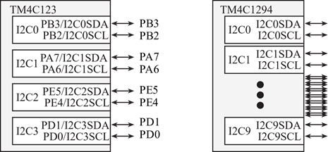
Figure T.6.2. I/O port pins for I2C on various TM4C/MSP432E4 microcontrollers.
There are seven steps to initialize I2C0 in master mode.
Step 1) we activate the I2C0 clock by setting bit 0 the SYSCTL_RCGCI2C_R register.
Step 2) Since I2C0 uses two pins on Port B, we need to activate Port B clock in register SYSCTL_RCGCGPIO_R.
Step 3) We connect I2C0 to pins PB3/PB2 by setting the alternative function. I.e., we set bits 2 and 3 of GPIO_PORTB_AFSEL_R register.
Step 4) I2C0 uses open drain mode on the data bit, so we set bit 3 of GPIO_PORTB_ODR_R register. The port will drive the line low when it wants to output a zero. Conversely, to make the line high, open drain mode causes the output to float and the pull-up resistor causes the line to go high. The SCL pin must not be configured as an open-drain signal, although the port causes it to act as if it were an open drain signal.
Step 5) We enable the digital circuits by setting 2 and 3 of GPIO_PORTB_DEN_R register.
Step 6) We enable master mode by setting the MFE bit in the I2C0_MCR_R register.
Step 7) Lastly, I2C0_MTPR_R is the I2C Master Timer Period Register, which determines the baud rate transferred as a master. It is the master's responsibility to generate the I2C clock. The timing of the I2C interface is derived from the bus clock. We set the baud rate by writing to the TPR field in the I2C0_MTPR_R register. Let fBUS be the frequency of the bus clock and let t =1/fBUS be the period of the bus clock. The I2C clock period (tbit) will be 20*(TPR+1)*t. In standard mode, we set the I2C clock frequency to be about 100 kHz (tbit =10 μs). In fast mode, we set the I2C clock frequency to be about 400 kHz. For example, to set the I2C to standard speed, assuming Δt is given in ns,
tbit = 20*(TPR+1)*t = 10000 ns
or TPR = 500/t -1
The R/S bit (bit 0) of the Master's Slave Address Register, I2C0_MSA_R, specifies whether the next data transfer will be a receive from slave (equals 1) or a write to slave (equals 0). Bits 7 through 1 of the Master's Slave Address Register contain the unique 7-bit address of the slave that the master is addressing. Generally, no two devices should have the same slave address. Many devices can permanently accept a new slave address from the master. I2C_MCS_ACK specifies whether or not the master acknowledges data received from the slave. I2C_MCS_ACK is only used when the I2C Bus is a receiver, not a transmitter.
When receiving data as a master, this bit determines if an acknowledgement will be sent during the 9th clock bit. 1 means an acknowledgement will be sent (Ack), and 0 means no acknowledgement will be sent (Nack). The master may not acknowledge the final byte sent by a slave. It must issue a STOP or repeated START condition after the negative acknowledge. The I2C module will always acknowledge address matches, provided it is enabled. A START or repeated start (RESTART) will be sent if software writes a 1 to the I2C_MCS_START bit, provided this microcontroller is the current bus master. Attempting a repeated start when the bus is owned by another master will result in loss of arbitration. I2C_MCS_START is part of the Master's Control/Status Register, which is a special register. Reads from this register return information about the master's status, and writes to this register control the master's next transmission. For example, set the I2C_MCS_ACK, I2C_MCS_STOP, and/or I2C_MCS_START bits and the I2C_MCS_RUN bit to begin the next transmission. Afterwards, read the I2C_MCS_ARBLST or I2C_MCS_ERROR bits to see if the master has lost arbitration of the bus. Many applications may also require reading the I2C_MCS_ADRACK and I2C_MCS_DATACK bits to ensure that the slave has acknowledged its address and any data. An unresponsive device may represent a serious hardware problem to which the system must react.
The master can be in three modes: idle, transmit and receive. Table T.6.2 summarizes the modes and operation of I2C. Combinations not listed in this table are either illegal or no operation.
|
State |
R/S |
ACK |
STOP |
START |
Run |
Action (and new state) |
|
Idle |
0 |
X |
0 |
1 |
1 |
START condition followed by SEND (goes to Master Transmit) |
|
0 |
X |
1 |
1 |
1 |
START condition followed by a SEND and STOP condition (remains in Idle). |
|
|
1 |
0 |
0 |
1 |
1 |
START condition, RECEIVE operation with negative ACK (goes to the Master Receive) |
|
|
1 |
0 |
1 |
1 |
1 |
START condition followed by RECEIVE and STOP condition (remains in Idle state) |
|
|
1 |
1 |
0 |
1 |
1 |
START condition followed by RECEIVE (goes to the Master Receive state) |
|
|
|
|
|
|
|
|
|
|
Master Transmit |
X |
X |
0 |
0 |
1 |
SEND operation (remains in Master Transmit state) |
|
X |
X |
1 |
0 |
0 |
STOP condition (goes to Idle state) |
|
|
X |
X |
1 |
0 |
1 |
SEND followed by STOP condition (goes to Idle state) |
|
|
0 |
X |
0 |
1 |
1 |
Repeated START condition followed by a SEND (remains in Master Transmit state) |
|
|
0 |
X |
1 |
1 |
1 |
Repeated START condition followed by SEND and STOP condition (goes to Idle state) |
|
|
1 |
0 |
0 |
1 |
1 |
Repeated START, then RECEIVE operation with a negative ACK (goes to Master Receive state) |
|
|
1 |
0 |
1 |
1 |
1 |
Repeated START condition followed by a SEND and STOP condition (goes to Idle state) |
|
|
1 |
1 |
0 |
1 |
1 |
Repeated START condition followed by RECEIVE (goes to Master Receive state) |
|
|
|
|
|
|
|
|
|
|
Master Receive |
X |
0 |
0 |
0 |
1 |
RECEIVE operation with negative ACK (remains in Master Receive state) |
|
X |
X |
1 |
0 |
0 |
STOP condition (goes to Idle state) |
|
|
X |
0 |
1 |
0 |
1 |
RECEIVE followed by STOP condition (goes to Idle state) |
|
|
X |
1 |
0 |
0 |
1 |
RECEIVE operation (remains in Master Receive state) |
|
|
1 |
0 |
0 |
1 |
1 |
Repeated START, then RECEIVE operation with a negative ACK (remains in Master Receive state). |
|
|
1 |
0 |
1 |
1 |
1 |
Repeated START, then RECEIVE and STOP condition (goes to Idle state) |
|
|
1 |
1 |
0 |
1 |
1 |
Repeated START condition followed by RECEIVE (remains in Master Receive state) |
|
|
0 |
X |
0 |
1 |
1 |
Repeated START condition followed by SEND (goes to Master Transmit state) |
|
|
0 |
X |
1 |
1 |
1 |
Repeated START condition followed by SEND and STOP condition (goes to Idle state) |
Table T.6.2. I2C commands, actions, and state changes.
Figure T.6.2 and Table T.6.3 describe the timing of I2C. Let tbit be the I2C period as defined by the bus clock and the TPR field in the I2C0_MTPR_R register. Because SCL and SDA are open-drain-type outputs, which the controller can only actively drive low. The setup time, tsetup, is the time before the rise of SCL that the data on SDA will be valid. The data remains valid throughout the time SCL is high. The hold time, thold, is the time after the fall of SCL that the data on SDA continues to be valid. The rise time, trise, of SDA and SCL depends on external signal capacitance and pull-up resistor values. The fall time, tfall, is specified up to a maximum 50 pF load.

Figure T.6.3. I2C timing intervals.
|
Parameter |
Minimum |
Typical |
Maximum |
|
tstart |
36 t |
|
|
|
thigh |
24 t |
|
|
|
tlow |
36 t |
|
|
|
tsetup |
18 t |
|
|
|
thold |
2 t |
|
|
|
trise |
** |
** |
** |
|
tfall |
|
9 ns |
10 ns |
|
tstop |
24 t |
|
|
Table T.6.3. I2C timing intervals, where t is the system bus period (** depends on external factors).
The objective of this example is to present a low-level device driver for an I2C network where this microcontroller is the only master, as shown in Program T.6.1. This simple example will employ busy-wait synchronization. I2C_Init first enables the I2C interface, starting out in master mode. Since this is the only master, it does not need to initialize any of the slave mode settings.
// Assumes a 50 MHz bus clock, 20*(TPR+1)*20ns = 10us, with TPR=24
#define TPR (500/20 - 1)
void I2C_Init(void){
SYSCTL_RCGCI2C_R |= 0x0001; // activate I2C0
SYSCTL_RCGCGPIO_R |= 0x0002; // activate port B
while((SYSCTL_PRGPIO_R&0x0002)== 0){};// ready?
GPIO_PORTB_AFSEL_R |= 0x0C; // enable alt funct on PB2,3
GPIO_PORTB_ODR_R |= 0x08; // enable open drain on PB3
GPIO_PORTB_PCTL_R = (GPIO_PORTB_PCTL_R&0xFFFF00FF)+0x00003300; // I2C
GPIO_PORTB_DEN_R |= 0x0C; // enable digital I/O on PB2,3
I2C0_MCR_R = 0x00000010; // master function enable
I2C0_MTPR_R = TPR; // configure for
100 kbps clock
}
Program T.6.1. TM4C123 I2C initialization in single master mode.
Program T.6.2 contains the function I2C_Send2 that transmits two bytes to a slave, creating a transmission shown in Figure T.6.4.
Figure T.6.4. I2C transmission of two bytes from master to slave
In a system with multiple masters this should check to see if the bus is idle first. Because this system has just one master, the bus should be idle. However, the first line of the function makes certain that the I2C hardware is free and there is not already another transaction pending. By setting the I2C_MCS_START bit of the I2C Master Control/Status Register, I2C0_MCS_R, the microcontroller will create a START condition. In a system with multiple masters, it should check to see if it lost bus arbitration (I2C_MCS_ARBLST). The slave address (with bit 0 equal to 0) will be sent. The two data bytes are sent, then the STOP is issued. If there is a possibility the slave doesn't exist, data doesn't get acknowledged, or bus arbitration is lost then this program could have checked I2C_MCS_ERROR after each transfer.
uint32_t I2C_Send2(uint8_t slave, uint8_t data1, uint8_t data2){
while(I2C0_MCS_R&0x00000001){}; // wait for I2C ready
I2C0_MSA_R = (slave<<1)&0xFE; // MSA[7:1] is slave address
I2C0_MSA_R &= ~0x01; // MSA[0] is 0 for send
I2C0_MDR_R = data1&0xFF; // prepare first byte
I2C0_MCS_R = ( I2C_MCS_START // generate start/restart
| I2C_MCS_RUN); // no ack, no stop,master enable
while(I2C0_MCS_R&0x00000001){}; // wait for transmission done
// check error bits
if((I2C0_MCS_R&
(I2C_MCS_DATACK|I2C_MCS_ADRACK|I2C_MCS_ERROR)) != 0){
I2C0_MCS_R = I2C_MCS_STOP; // stop, no ack, disable
return (I2C0_MCS_R& // return error bits if nonzero
(I2C_MCS_DATACK|I2C_MCS_ADRACK|I2C_MCS_ERROR));
}
I2C0_MDR_R = data2&0xFF; // prepare second byte
I2C0_MCS_R = (I2C_MCS_STOP // no ack, stop, no start
| I2C_MCS_RUN); // master enable
while(I2C0_MCS_R&0x00000001){}; // wait for transmission done
return (I2C0_MCS_R& // return error bits
(I2C_MCS_DATACK|I2C_MCS_ADRACK|I2C_MCS_ERROR));
}
Program T.6.2. I2C transmission in single master mode.
Program T.6.3 contains the function I2C_Recv2 that receives two bytes from a slave, creating a transmission shown in Figure T.6.5.
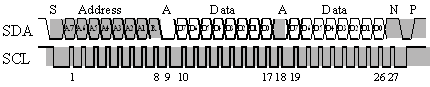
Figure T.6.5. I2C transmission of two bytes from slave to master.
By setting the I2C_MCS_START bit, the microcontroller will create a START condition. During the first transfer, the Tx/Rx bit is 1, so the slave address (with bit 0 equal to 1) will be sent, and the master goes into receive mode. During the next two transfers, the master is in receive mode, so data flows into the microcontroller. To trigger any data transfer, the software writes a valid value to I2C0_MCS_R with the I2C_MCS_RUN bit set. During the first data transfer I2C_MCS_ACK is 1, creating a positive acknowledgement. Conversely during the second data transfer I2C_MCS_ACK is 0, creating a negative acknowledgement and signaling to the slave that this is the last data to be transferred. The STOP is requested when the I2C_MCS_STOP bit of the I2C0_MCS_R register is set, and it automatically is issued after the final data transfer.
This is a simple concept that may seem complicated at first. Basically:
0) Initialize: turn on GPIOB and I2C modules, set up GPIOB pins, set up I2C master
1) Put slave address into I2C0_MSA_R[7:1]
2) (receive only) Set I2C0_MSA_R[0]
2) (transmit only) Clear I2C0_MSA_R[0] and put first byte into I2C0_MDR_R[7:0]
3) Write a valid value to I2C0_MCS_R[3:0] to start transfer
4) Wait for transfer to finish: while(I2C0_MCS_R&0x00000001){};
5) (receive only) Read first byte from I2C0_MDR_R[7:0]
6) repeat Steps 2-5 until done
Timing is complicated and potentially confusing. Fortunately, it is handled by hardware you are already given. There are two complicated things for which you are responsible. The first issue is understanding what codes to send to the I2C slave. The second complicated issue is Step 3. There are 4 bits to write to I2C0_MCS_R[3:0], and they depend on the master's current state and next state as described in Table T.6.2.
#define I2C_MCS_ACK 0x00000008 // Data Acknowledge Enable
#define I2C_MCS_ADRACK 0x00000004 // Acknowledge Address
#define I2C_MCS_STOP 0x00000004 // Generate STOP
#define I2C_MCS_START 0x00000002 // Generate START
#define I2C_MCS_ERROR 0x00000002 // Error
#define I2C_MCS_RUN 0x00000001 // I2C Master Enable
#define MAXRETRIES 5 // number of receive attempts before giving up
uint16_t I2C_Recv2(uint8_t slave){ uint8_t data1,data2;
int retryCounter = 1;
do{
while(I2C0_MCS_R&0x00000001){}; // wait for I2C ready
I2C0_MSA_R = (slave<<1)&0xFE; // MSA[7:1] is slave address
I2C0_MSA_R |= 0x01; // MSA[0] is 1 for receive
I2C0_MCS_R = ( I2C_MCS_ACK // positive data ack
| I2C_MCS_START // no stop, yes start/restart
| I2C_MCS_RUN); // master enable
while(I2C0_MCS_R&0x00000001){}; // wait for transmission done
data1 = (I2C0_MDR_R&0xFF); // MSB data sent first
I2C0_MCS_R = (I2C_MCS_STOP // generate stop, no start
| I2C_MCS_RUN); // master enable
while(I2C0_MCS_R&0x00000001){}; // wait for transmission done
data2 = (I2C0_MDR_R&0xFF); // LSB data sent last
retryCounter = retryCounter + 1; // increment retry counter
} // repeat if error
while(((I2C0_MCS_R&(I2C_MCS_ADRACK|I2C_MCS_ERROR)) != 0)
&& (retryCounter <= MAXRETRIES));
return (data1<<8)+data2; // usually returns 0xFFFF on error
}
Program T.6.3. I2C reception in single master mode.
Figure T.6.6 shows a logic analyzer measurement taken with Program T.6.3 communicating with a Texas Instruments TMP102 thermometer. The main program calls I2C_Recv2(0x48); The first transmission sends the 0x91 (slave address, read) command. It then receives two transmissions, which is the temperature encoded with 0.0625°C resolution.
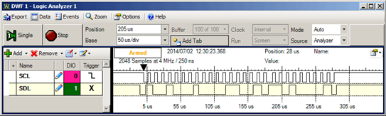
Figure T.6.6. Logic analyzer transmission of I2C_Recv2, with one output and two inputs.
I2C can be very difficult to configure. We suggest you observe the SCL and SDL on an oscilloscope. First check the clock rate and second verify the output high and output low voltages are within specification. Look up VIH and VIL of both the microcontroller and the remote sensor. The high voltage measured by the scope should be higher than VIH of both devices. The low voltage measured by the scope should be lower than VIL of both devices.
T.7. Edge-triggered Interrupts
We will begin with a simple example that counts the number of rising edges on Port C bit 4, as shown in Program T.7.1. The initialization requires many steps. (a) The clock for the port must be enabled. (b) The global variables should be initialized. This step also allows the clock to stabilize. (c) The appropriate pins must be enabled as inputs. (d) We must specify whether to trigger on the rise, the fall, or both edges. In this case we will trigger on the rise of PC4. (e) It is good design to clear the trigger flag during initialization so that the first interrupt occurs due to the first rising edge after the initialization has been run. We do not wish to trigger on a rising edge that might have occurred during the power up phase of the system. (f) We arm the edge-trigger by setting the corresponding bits in the IM register. (g) We establish the priority of Port C by setting bits 23 - 21 in the NVIC_PRI0_R register as listed in Table T.7.1. We activate Port C interrupts in the NVIC by writing a one to bit 2 in the NVIC_EN0_R register. This initialization is shown to enable interrupts in step (i). However, in most systems we would not enable interrupts in the device initialization. Rather, it is good design to initialize all devices in the system, then enable interrupts. On the TM4C we also clear the corresponding bits in AMSEL and PCTL.
volatile uint32_t FallingEdges = 0;
void EdgeCounter_Init(void){
SYSCTL_RCGCGPIO_R |= 0x04; // (a) activate clock for Port C
FallingEdges = 0; // (b) initialize counter
GPIO_PORTC_DIR_R &= ~0x10; // (c) make PC4 in
GPIO_PORTC_DEN_R |= 0x10; // enable digital I/O on PC4
GPIO_PORTC_IS_R &= ~0x10; // (d) PC4 is edge-sensitive
GPIO_PORTC_IBE_R &= ~0x10; // PC4 is not both edges
GPIO_PORTC_IEV_R &= ~0x10; // PC4 falling edge event
GPIO_PORTC_ICR_R = 0x10; // (e) clear flag4
GPIO_PORTC_IM_R |= 0x10; // (f) arm interrupt on PC4
NVIC_PRI0_R = (NVIC_PRI0_R&0xFF00FFFF)|0x00A00000; // (g) priority 5
NVIC_EN0_R = 4; // (h) enable interrupt 2 in NVIC
// Enable interrupts in the main // (i) I=0
}
void GPIOPortC_Handler(void){
GPIO_PORTC_ICR_R = 0x10; // acknowledge flag4
FallingEdges = FallingEdges + 1;
}
Program T.7.1. Interrupt-driven edge-triggered input that counts rising edges of PC4.
Edge-triggered interrupts can be generated with all six ports. Table T.7.1 shows the changes one must make to use the other ports.
| Register | PortA | PortB | PortC | PortD | PortE | PortF |
| SYSCTL_RCGCGPIO_R | bit 0 | bit 1 | bit 2 | bit 3 | bit 4 | bit 5 |
| Priority register | NVIC_PRI0_R | NVIC_PRI0_R | NVIC_PRI0_R | NVIC_PRI0_R | NVIC_PRI1_R | NVIC_PRI7_R |
| Priority bits | 7-5 | 15-13 | 23-21 | 31-29 | 7-5 | 23-21 |
| Enable register | NVIC_EN0_R | NVIC_EN0_R | NVIC_EN0_R | NVIC_EN0_R | NVIC_EN0_R | NVIC_EN0_R |
| Enable bit | 0 | 1 | 2 | 3 | 4 | 30 |
Table T.7.1. Changes to Program T.7.1 needed to use the six GPIO ports.
All ISRs must acknowledge the interrupt by clearing the trigger flag that requested the interrupt. For edge-triggered PC4, the trigger flag is bit 4 of the GPIO_PORTC_RIS_R register. This flag can be cleared by writing a 0x10 to GPIO_PORTC_ICR_R.
If two or more triggers share the same vector, these requests are called polled interrupts, and the ISR must determine which trigger generated the interrupt. If the requests have separate vectors, then these requests are called vectored interrupts and the ISR knows which trigger caused the interrupt.
In this example, we will Interface two switches and signal associated semaphores when each switch is pressed. We will assume the switches do not bounce (interfacing switches that bounce will be covered later in the chapter). The semaphore SW1 will be signaled when switch SW1 is pressed, and similarly, semaphore SW2 will be signed when switch SW2 is pressed. In the first solution, we will use vectored interrupts by connecting one switch to Port C and the other switch to Port E. Since the two sources have separate vectors, the switch on Port C will automatically activate GPIOPortC_Handler and switch on Port E will automatically activate GPIOPortE_Handler. The left side of Figures T.7.1 and T.7.2 show the solution with vectored interrupts.
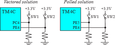
Figure T.7.1. Interface circuits for two solutions of switch-triggered interrupts.
The software solution using vectored interrupts is in Program T.7.2. We initialize two I/O pins as inputs with rising edge interrupt triggers. In this way, we get an interrupt request when the switch is touched. I.e., an interrupt occurs on the 0 to 1 rising edge either of PC4 or PE4. To acknowledge an interrupt we clear the trigger flag. Writing a 0x10 to the flag register, GPIO_PORTn_ICR_R, will clear bit 4 without affecting the other bits in the register. Notice that the acknowledgement uses an "=" instead of an "|=".
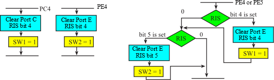
Figure T.7.2. Flowcharts for a vectored and polled interrupt.
volatile uint32_t SW1, SW2; // semaphores
void VectorButtons_Init(void){
SYSCTL_RCGCGPIO_R |= 0x14; // activate clock for Ports C and E
SW1 = 0; // clear semaphores
SW2 = 0;
GPIO_PORTC_DIR_R &= ~0x10; // make PC4 in (PC4 built-in button)
GPIO_PORTC_DEN_R |= 0x10; // enable digital I/O on PC4
GPIO_PORTC_IS_R &= ~0x10; // PC4 is edge-sensitive (default setting)
GPIO_PORTC_IBE_R &= ~0x10; // PC4 is not both edges (default setting)
GPIO_PORTC_IEV_R |= 0x10; // PC4 rising edge event
GPIO_PORTC_ICR_R = 0x10; // clear flag4
GPIO_PORTC_IM_R |= 0x10; // arm interrupt on PC4
NVIC_PRI0_R = (NVIC_PRI0_R&0xFF00FFFF)|0x00400000; // PortC=priority 2
GPIO_PORTE_DIR_R &= ~0x10; // make PE4 in (PE4 button)
GPIO_PORTE_DEN_R |= 0x10; // enable digital I/O on PE4
GPIO_PORTE_IS_R &= ~0x10; // PE4 is edge-sensitive (default setting)
GPIO_PORTE_IBE_R &= ~0x10; // PE4 is not both edges (default setting)
GPIO_PORTE_IEV_R |= 0x10; // PE4 rising edge event
GPIO_PORTE_ICR_R = 0x10; // clear flag4
GPIO_PORTE_IM_R |= 0x10; // arm interrupt on PE4
NVIC_PRI1_R = (NVIC_PRI1_R&0xFFFFFF00)|0x00000040; // PortE=priority 2
NVIC_EN0_R = (NVIC_EN0_INT2+NVIC_EN0_INT4); // enable interrupts 2,4
// Enable interrupts in the main
}
void GPIOPortC_Handler(void){
GPIO_PORTC_ICR_R = 0x10; // acknowledge flag4
SW1 = 1; // signal SW1 occurred
}
void GPIOPortE_Handler(void){
GPIO_PORTE_ICR_R = 0x10; // acknowledge flag4
SW2 = 1; // signal SW2 occurred
}
Program T.7.2. Example of a vectored interrupt.
The right sides of Figures T.7.1 and T.7.2 show the solution with polled interrupts. Touching either switch will cause a Port E interrupt. The ISR must poll to see which one or possibly both caused the interrupt. Fortunately, even though they share a vector, the acknowledgements are separate. The code GPIO_PORTE_ICR_R=0x10; will clear bit 4 in the status register without affecting bit 5, and the code GPIO_PORTE_ICR_R=0x20; will clear bit 5 in the status register without affecting bit 4. This means the timing of one switch does not affect whether or not pushing the other switch will signal its semaphore. On the other hand, whether we are using polled or vectored interrupt, because there is only one processor, the timing of one interrupt may delay the servicing of another interrupt.
The polled solution is Program T.7.3. It takes three conditions to cause an interrupt. 1) The PE4 and PE5 are armed in the initialization; 2) The TM4C is enabled for interrupts with the EnableInterrupts() function; 3) The trigger GPIO_PORTE_RIS_R is set on the rising edge of PE4 or the trigger GPIO_PORTE_RIS_R is set on the rising edge of PE5. Because the two triggers have separate acknowledgments, if both triggers are set, both will get serviced. Furthermore, the polling sequence does not matter.
volatile uint8_t SW1, SW2;
void PolledButtons_Init(void){
SYSCTL_RCGCGPIO_R |= 0x10; // activate clock for Port E
SW1 = 0; SW2 = 0; // clear semaphores
GPIO_PORTE_DIR_R &= ~0x30; // make PE5-4 in (PE5-4 buttons)
GPIO_PORTE_DEN_R |= 0x30; // enable digital I/O on PE5-4
GPIO_PORTE_IS_R &= ~0x30; // PE5-4 is edge-sensitive
GPIO_PORTE_IBE_R &= ~0x30; // PE5-4 is not both edges
GPIO_PORTE_IEV_R |= 0x30; // PE5-4 rising edge event
GPIO_PORTE_ICR_R = 0x30; // clear flag5-4
GPIO_PORTE_IM_R |= 0x30; // arm interrupts on PE5-4
NVIC_PRI1_R = (NVIC_PRI1_R&0xFFFFFF00)|0x00000040; // PortE=priority 2
NVIC_EN0_R = NVIC_EN0_INT4; // enable interrupt 4 in NVIC
// Enable interrupts in the main
}
void GPIOPortE_Handler(void){
if(GPIO_PORTE_RIS_R&0x10){ // poll PE4
GPIO_PORTE_ICR_R = 0x10; // acknowledge flag4
SW1 = 1; // signal SW1 occurred
}
if(GPIO_PORTE_RIS_R&0x20){ // poll PE5
GPIO_PORTE_ICR_R = 0x20; // acknowledge flag5
SW2 = 1; // signal SW2 occurred
}
}
Program T.7.3. Example of a polled interrupt.
T.8. Pulse Width Modulation
Generating output waves is an essential task for real-time systems, so microcontrollers have multiple methods to create digital output waves.
T.8.1. Pulse Width Modulation using the Timer Module
Pulse width modulation is an effective and thus popular mechanism for the embedded microcontrollers to control external devices. The timer can create PWM outputs by setting the TAAMS bit and selecting periodic mode in TAMR field in the TIMER0_TAMR_R register. The output is one for High cycles then zero for Low cycles. This example generates a variable duty cycle square wave using output compare. Output compare events will again be requested at a rate twice as fast as the resulting square wave frequency. One event is required for the rising edge and another for the falling edge. In the examples below, we make High plus Low be a constant. By adjusting the ratio of High and Low the software can control the duty cycle.
![]()
This implementation occurs in hardware and does not require interrupts. Therefore, it can generate waves close to 0 or 100% duty cycle. If we clear the TAPWML bit of the control register we select normal PWM mode. In normal mode, the corresponding output pin is set when the timer is loaded with the value in the TIMER0_TAILR_R register. When it reaches the value stored in the TIMER0_TAMATCHR_R register, the pin is cleared. The TAPWML bit of the control register inverts this behavior. In all modes, the timer is reloaded with the value in the TIMER0_TAILR_R register on the cycle after it reaches 0x0000. In PWM output mode, the timer continues counting indefinitely until explicitly disabled by clearing the TAEN (or TBEN) bit in the TIMER0_CTL_R register. Figure T.8.1 shows the PWM output can be used to interface a DC motor to the microcontroller.
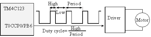
Figure T.8.1. The PWM output of Timer 0A can adjust the power to the DC motor.
Program T.8.1 configures Timer 0A for PWM output. The user calls PWM_Init once to turn it on, and then calls PWM_Duty to adjust the duty cycle.
// period is number of bus clock cycles in the PWM period
// high is number of bus clock cycles the signal is high
void PWM_Init(uint16_t period, uint16_t high){
SYSCTL_RCGCTIMER_R |= 0x01; // activate timer0
SYSCTL_RCGCGPIO_R |= 0x02; // activate port B
while((SYSCTL_PRGPIO_R&0x02) == 0){};
GPIO_PORTB_AFSEL_R |= 0x40; // enable alt funct on PB6
GPIO_PORTB_DEN_R |= 0x40; // enable digital I/O on PB6
GPIO_PORTB_PCTL_R = (GPIO_PORTB_PCTL_R&0xF0FFFFFF)+0x07000000;
TIMER0_CTL_R &= ~0x00000001; // disable timer0A during setup
TIMER0_CFG_R = 0x00000004; // configure for 16-bit timer mode
TIMER0_TAMR_R = 0x0000000A; // PWM and periodic mode
TIMER0_TAILR_R = period-1; // timer start value
TIMER0_TAMATCHR_R = period-high-1; // duty cycle = high/period
TIMER0_CTL_R |= 0x00000001; // enable timer0A 16-b, PWM
}
void PWM_Duty(uint16_t high){ // duty cycle is high/period
TIMER0_TAMATCHR_R = TIMER0_TAILR_R-high; // duty cycle = high/period
}
Program T.8.1. Software to generate a PWM output using Timer 0A.
: What event in the timer makes PB6 go high?
: What event in the timer makes PB6 go low?
T.8.2. Pulse Width Modulation using the PWM Module
PWM outputs are so important that many microcontrollers have dedicated PWM modules. The number of PWMs and associated pins vary from one microcontroller to the next, see Figure T.8.2. The TM4C123 has sixteen. See Table T.4.1 for PCTL settings.
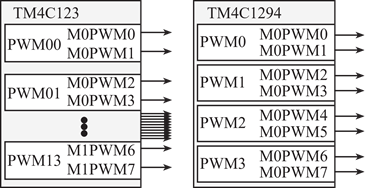
Figure T.8.2. PWM pins on the TM4C123.
The PWM0 block produces the PWM0 and PWM1 outputs, the PWM1 block produces the PWM2 and PWM3 outputs, the PWM2 block produces the PWM4 and PWM5 outputs, and the PWM3 on the TM4C123 block produces the PWM6 and PWM7 outputs. The TM4C123 has a second block providing for an additional eight PWM outputs. The design of a PWM system considers three factors. The first factor is the period of the PWM output. Most applications choose a period, initialize the waveform at that period, and adjust the duty cycle dynamically. The second factor is precision, which is the total number of duty cycles that can be created. A 16-bit channel can potentially create up to 65536 different duty cycles. However, since the duty cycle register must be less than or equal to the period register, the precision of the system is determined by the value written to the period register. The last consideration is the number of channels. The RSLK robot uses two PWM outputs to set the power delivered to the motor. For more information on the RSLK motor interface, see Section 8.3.5
Program T.8.2 shows the initialization on a TM4C123 for generating a PWM on the PB6/PWM0 pin. 1) First, we activate the clock for the PWM module. 2) Second, we activate the output pin as a digital alternate function. 3) Next, we select the clock to be used for the PWM in RCC register. If we do not use the PWM divider, then it is clocked from the bus clock. With the divider we can choose /2, /4, /8, /16, /32, or /64. Assuming the TM4C123 is running at 80 MHz, this program specifies the PWM clock to be 80/4= 20MHz. 4) We set the PWM to countdown mode. We specify in the PWM_0_GENA_R register that the comparator action is to set to one, and the load action is set to zero. 5) We specify the period in the PWM_0_LOAD_R register. 6) We specify the duty cycle in the PWM_0_CMPA_R register. 7) Lastly, we start and enable the PWM. We call PWM0_Init once to turn it on, and then call PWM0_Duty to adjust the duty cycle. Assume the PWM clock is 20MHz, we call PWM0_Init(40000,20000); to create a 0.5 ms period 50 % duty cycle output on PWM0 (PB6). PB6 goes low on LOAD, and PB6 goes high on CMPA.
// period is 16-bit number of PWM clock cycles in one period (3<=period)
// duty is number of PWM clock cycles output is high (2<=duty<=period-1)
// PWM clock rate = processor clock rate/SYSCTL_RCC_PWMDIV
// = BusClock/2 (in this example)
void PWM0_Init(uint16_t period, uint16_t duty){
SYSCTL_RCGCPWM_R |= 0x01; // 1) activate PWM0
SYSCTL_RCGCGPIO_R |= 0x02; // 2) activate port B
while((SYSCTL_PRGPIO_R&0x02) == 0){};
GPIO_PORTB_AFSEL_R |= 0x40; // enable alt funct on PB6
GPIO_PORTB_PCTL_R = (GPIO_PORTB_PCTL_R&0xF0FFFFFF)+0x04000000; // PWM0
GPIO_PORTB_AMSEL_R &= ~0x40; // disable analog fun on PB6
GPIO_PORTB_DEN_R |= 0x40; // enable digital I/O on PB6
SYSCTL_RCC_R = 0x00120000 | // 3) use PWM divider
(SYSCTL_RCC_R & (~0x000E0000)); // configure for /4 divider
PWM0_0_CTL_R = 0; // 4) re-loading down-counting mode
PWM0_0_GENA_R = 0xC8; // low on LOAD, high on CMPA down
PWM0_0_LOAD_R = period - 1; // 5) cycles needed to count down to 0
PWM0_0_CMPA_R = duty - 1; // 6) count value when output rises
PWM0_0_CTL_R |= 0x00000001; // 7) start PWM0
PWM0_ENABLE_R |= 0x00000001; // enable PB6/M0PWM0
}
void PWM0_Duty(uint16_t duty){
PWM0_0_CMPA_R = duty - 1; // 6) count value when output rises
}
Program T.8.2. Implementation of a 16-bit PWM output. low on LOAD, high on CMPA.
: With a PWM initialization of PWM0_Init(40000,20000); what is the precision of the PWM output?
T.9. Input Capture Details on the TM4C
T.9.1. Input Capture Concepts
The Texas Instruments microcontrollers have timers that are separate and distinct from SysTick, see Figure T.9.1. Input edge time mode (or input capture mode) is used to make time measurements on input signals. We can use input capture to measure the period or pulse width of digital-level signals. The input capture system can also be used to trigger interrupts on rising or falling transitions of external signals. A General Purpose Timer Module (GPTM) has two 16-bit timers, which can be extended to 24 bits. Each GPTM input capture module has
An external input pin, e.g., CCP0
A trigger flag bit, called Raw Interrupt Status, e.g., CAERIS
Two edge control bits, Event bits, e.g., TAEVENT
An arm bit, called interrupt mask, e.g., CAEIM
A 16-bit or 24-bit input capture register, e.g., TAR
The various members of the TM4C family have from zero to twelve input capture modules. Figure T.9.1 shows the port pins used for input capture vary from microcontroller to microcontroller. The input capture and output compare pins are labeled CCP0, CCP1, ... A timer module has associated I/O pins. The even CCP pin is attached to Submodule A and the odd pin to Submodule B. Table T.4.1 shows the PCTL constants, identifying the pins that can be input capture on the TM4C123.
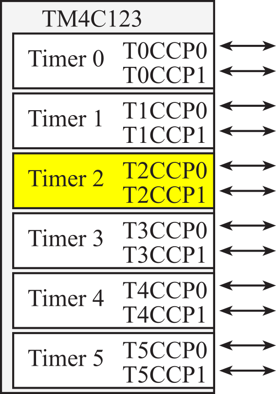
Figure T.9.1. Input capture pins on the TM4C123 are called TnCCP0 and TnCCP1.
In this book we use the term arm to describe the bit that allows/denies a specific flag from requesting an interrupt. The Texas Instruments manuals refer to this bit as a mask. I.e., the device is armed when the mask bit is 1. Typically, there is a separate arm bit for every flag that can request an interrupt. An external digital signal is connected to the input capture pin. During initialization we specify whether the rising or falling edge of the external signal will trigger an input capture event. The 16-bit counter decrements at the rate of the bus clock, when it hits 0, it automatically rolls over to 0xFFFF and continues to count down (Figure T.9.2). Two or three actions result from an input capture event: 1) the current timer value is copied into the input capture register (TAR or TBR), 2) the input capture flag is set (RIS) and 3) an interrupt is requested if armed (IM). This means an interrupt can be requested on a capture event. When using the prescaler on the TM4C, the counter can be extended to 24 bits.
The input capture mechanism has many uses. For input capture, an external digital signal is connected to an input (TnCCP0 or TnCCP1) of the microcontroller. Three of common applications are:
1. An ISR is executed on the active edge of the external signal
2. Perform two rising edge input captures and subtract the two to get period
3. Perform a rising edge and then a falling edge capture and subtract the two measurements to get pulse width
|
|
31-3 |
2-0 |
Name |
||||||
|
40030000 |
|
GPTMCFG |
TIMER0_CFG |
||||||
|
|
|
|
|
|
|
|
|
|
|
|
|
31-4 |
3 |
2 |
1-0 |
|
||||
|
40030004 |
|
TAAMS |
TACMR |
TAMR |
_TAMR_R |
||||
|
|
|
|
|
|
|
|
|
|
|
|
|
31-4 |
3 |
2 |
1-0 |
|
||||
|
40030008 |
|
TBAMS |
TBCMR |
TBMR |
_TBMR_R |
||||
|
|
|
|
|
|
|
|
|
|
|
|
|
14 |
13 |
11-10 |
8 |
6 |
5 |
3-2 |
0 |
|
|
4003000C |
TBPWML |
TBOTE |
TBEVENT |
TBEN |
TAPWML |
TAOTE |
TAEVENT |
TAEN |
_CTL_R |
|
|
|
|
|
|
|
|
|
|
|
|
|
31-11 |
10 |
9 |
8 |
7-4 |
2 |
1 |
0 |
|
|
40030018 |
|
CBEIM |
CBMIM |
TBTOIM |
|
CAEIM |
CAMIM |
TATOIM |
_IMR_R |
|
|
|
|
|
|
|
|
|
|
|
|
|
31-11 |
10 |
9 |
8 |
7-4 |
2 |
1 |
0 |
|
|
4003001C |
|
CBERIS |
CBMRIS |
TBTORIS |
|
CAERIS |
CAMRIS |
TATORIS |
_RIS_R |
|
|
|
|
|
|
|
|
|
|
|
|
|
31-11 |
10 |
9 |
8 |
7-4 |
2 |
1 |
0 |
|
|
40030020 |
|
CBEMIS |
CBMMIS |
TBTOMIS |
|
CAEMIS |
CAMMIS |
TATOMIS |
_MIS_R |
|
|
|
|
|
|
|
|
|
|
|
|
|
31-11 |
10 |
9 |
8 |
7-4 |
2 |
1 |
0 |
|
|
40030020 |
|
CBECINT |
CBMCINT |
TBTOCINT |
|
CAECINT |
CAMCINT |
TATOCINT |
_ICR_R |
|
|
|
|
|
|
|
|
|
|
|
|
|
31-16 |
15-0 |
|
||||||
|
40030028 |
TAILRH |
TAILRL |
_TAILR_R |
||||||
|
|
|
|
|
||||||
|
|
31-16 |
15-0 |
|
||||||
|
4003002C |
|
TBILRL |
_TBILR_R |
||||||
|
|
|
|
|
||||||
|
|
31-16 |
15-0 |
|
||||||
|
40030030 |
TAMRH |
TAMRL |
TAMATCHR |
||||||
|
|
|
|
|
||||||
|
|
31-16 |
15-0 |
|
||||||
|
40030034 |
|
TBMRL |
TBMATCHR |
||||||
|
|
|
|
|
|
|
|
|
|
|
|
|
31-8 |
7-0 |
|
||||||
|
40030038 |
|
TAPSR |
_TAPR_R |
||||||
|
|
|
|
|
||||||
|
|
31-8 |
7-0 |
|
||||||
|
4003003C |
|
TBPSR |
_TBPR_R |
||||||
|
|
|
|
|
||||||
|
|
31-8 |
7-0 |
|
||||||
|
40030040 |
|
TAPSMR |
_TAPMR_R |
||||||
|
|
|
|
|
||||||
|
|
31-8 |
7-0 |
|
||||||
|
40030044 |
|
TBPSMR |
_TBPMR_R |
||||||
|
|
|
|
|
|
|
|
|
|
|
|
|
31-16 |
15-0 |
|
||||||
|
40030048 |
TARH |
TARL |
_TAR_R |
||||||
|
|
|
|
|
||||||
|
|
31-16 |
15-0 |
|
||||||
|
4003004C |
|
TBRL |
_TBR_R |
||||||
Table T.9.1. Timer0 registers. Each register is 32 bits wide. Shaded bits are zero. The bits shown in bold will be used in this section. Timers 1, 2, ... have the same formats.
There are also 32-bit timers, called wide timers, which can be extended to 48 bits. However, in this book, we will only present the 32-bit timers.
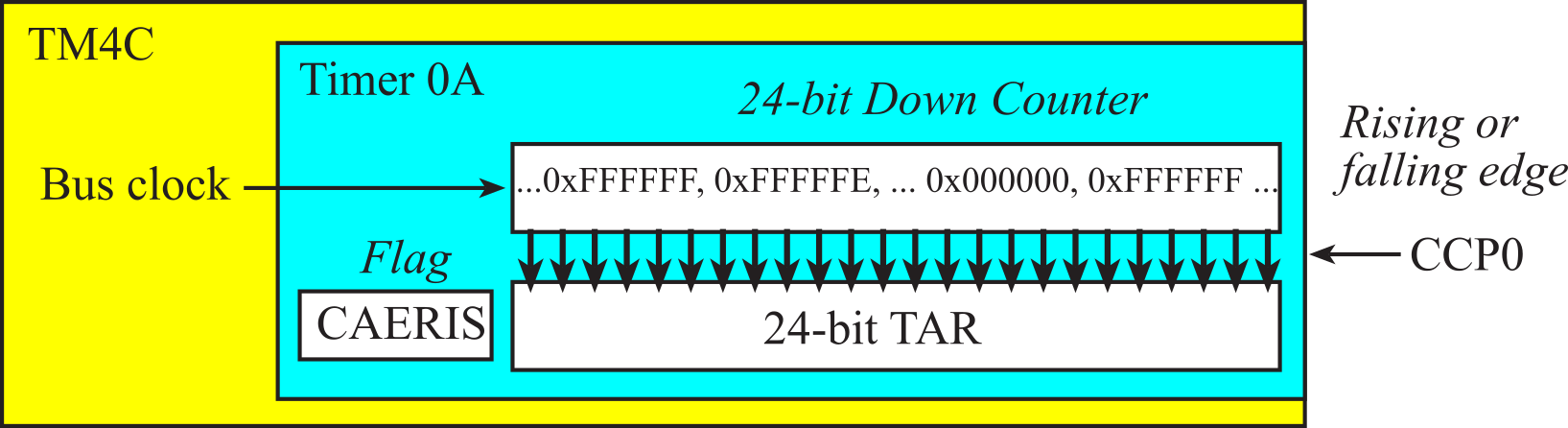
Figure T.9.2. Rising or falling edge of CCP0 causes the counter to be latched into TAR, setting CAERIS.
Observation: The timer is very accurate because of the stability of the crystal clock.
Observation: When measuring period or pulse-width, the measurement resolution will equal the bus clock period.
T.9.2. Period Measurement
The basic idea of period measurement is to generate two input captures on the same edge (both rise or both fall), record the times of each edge, and calculate the period as the difference between those two times. Before one implements a system that measures period, it is appropriate to consider the issues of resolution, precision and range. The resolution of a period measurement is defined as the smallest change in period that can reliably be detected. In Example T.9.2, the bus clock is 80 MHz. This means, if the period increases by 12.5 ns, then there will be one more Timer clock between the first rising edge and the second rising edge. In this situation, the 24-bit subtraction will increase by 1, therefore the period measurement resolution is 12.5 ns. The resolution is the smallest measurable change. Resolution defines the units of the measurement. In this first example, if the calculation of Period results in 1000, then it represents a period of 1000*12.5ns or 12.5µs. The precision of the period measurement is defined as the number of separate and distinguishable measurements. If the 24-bit counter is used, there are about 16 million different periods that can be measured. We can specify the precision in alternatives, e.g., 224, or in bits, e.g., 24 bits. The last issue to consider is the range of the period measurement, which is defined as the minimum and maximum values that can reliably be measured. We are concerned what happens if the period is too small or too large. A good measurement system should be able to detect overflows and underflows. In addition, we would not like the system to crash, or hang-up if the input period is out of range. Similarly, it is desirable if the system can detect when there is no period. For edge detection, the input must be high for at least two system clock periods and low for at least two system clock periods.
Table T.9.1 shows some of the registers for Timer 0. We begin initialization by enabling the clock for the timer and for the digital port we will be using. We enable the digital pin and select its alternative function. We will disable the timer during initialization by clearing the TAEN (or TBEN) bit in the TIMER0_CTL_R register. To use 16-bit mode, we set GPTMCFG field to 4. We clear the TAAMS (or TBAMS) bit for capture mode. We set the TACMR (or TBCMR) bit for input edge time mode. The TAMR (or TBMR) field is set to 3 for capture mode. In summary, we write a 0x0007 to the TIMER0_TAMR_R register to select input capture mode. Table T.9.2 lists the edge capture modes for TAEVENT (or TBEVENT.)
|
TAEVENT |
Active edge |
|
00 |
Capture on rising |
|
01 |
Capture on falling |
|
10 |
Reserved |
|
11 |
Capture on both rising and falling |
Table T.9.2. Two control bits define the active edge used for input capture (TBEVENT is the same) .
When we are measuring time with prescaler, such as period measurement and pulse width measurement, we set the 24-bit reload value to 0xFFFFFF. In this way, the 24-bit subtraction of two capture events yields the time difference between events. In particular, we will initialize TIMER0_TAILR_R to 0xFFFF and TIMER0_TAPR_R to 0xFF. We arm the input capture by setting the CAEIM (or CBEIM) bit in the TIMER0_IMR_R register. It is good practice to clear the trigger flag in the initialization so that the first interrupt occurs do to actions occurring after the initialization, and not due to edges that might have occurred during power up. The trigger flags are in the TIMER0_RIS_R register. These flags are cleared by writing 1's into corresponding bits in the TIMER0_ICR_R register. After all configuration bits are set, the Timer can be enabled by setting the TAEN (or TBEN) bit in the TIMER0_CTL_R register. If interrupts are required, then the NVIC must be configured by setting the priority and enabling the appropriate interrupt number.
There is an 8-bit prescaler defined for each submodules A and B: TIMER0_TAPMR_R and TIMER0_TBPMR_R. The prescalers on the TM4C are used to extend the 16-bit timer to 24 bits.
The TAEVENT bits of TIMER0_CTL_R register specify whether the rising or falling edge of CCP0 will trigger an input capture event on Timer 0A. Two or three actions result from an input capture event: 1) the current timer value is copied into the input capture register, TIMER0_TAR_R, 2) the input capture flag (CAERIS) is set, and 3) an interrupt is requested if the mask bit (CAEIM) is 1. The CAERIS and CBERIS flag bits in the TIMER0_RIS_R register do not behave like a regular memory location. In particular, the flag cannot be set by software. Rather, an input capture or output compare hardware event will set the flag. The other peculiar behavior of the flag is that the software must write a one to the TIMER0_ICR_R register to clear the flag. If the software writes a zero to the TIMER0_ICR_R register, no change will occur. From Table T.9.1, we see the CAERIS trigger flag is in bit 2 of the TIMER0_RIS_R register. The proper way to clear this trigger flag is
TIMER0_ICR_R = 0x0004;
Writes the TIMER0_RIS_R register have no effect. No effect occurs in the bits to which we write a zero in the TIMER0_ICR_R register.
Observation: The phase-lock-loop (PLL) on the ARM will affect the timer period.
T.9.3. Pulse width measurement
24-bit pulse width measurement. Design a system to measure pulse width using interrupts, with a precision of 24 bits and a resolution of 12.5 ns. In this example, the digital-level input signal is connected to two input capture pins, CCP0 and CCP1 (Figure T.9.3). The bus clock is selected to be 80 MHz so the measurement resolution will be 12.5 ns. The rising edge time will be measured by Timer0B without the need of an interrupt and the falling edge interrupts will be handled by Timer0A. The pulse width is calculated as the difference in TIMER0_TBR_R-TIMER0_TAR_R latch values. In this example the Timer0A interrupt handler simply sets the global variable, PW, at the time of the falling edge. Because no software is required to process the Timer0B measurement, there is no software limit to the minimum pulse width. There is the hardware limit requiring at least two bus clock periods while high and two bus clock periods while low. On the other hand, software processing is required to handle the Timer0A signal, so there is a minimum period. E.g., there must be more than 2 µs from one falling edge to the next falling edge. This time depends on software execution speed in the ISR, and the context switch. This minimum period will be larger for systems with higher priority interrupts. Again, the first measurement may or may not be accurate. Note: remove R9 and R10 on the LaunchPad to use PB6 and PB7.
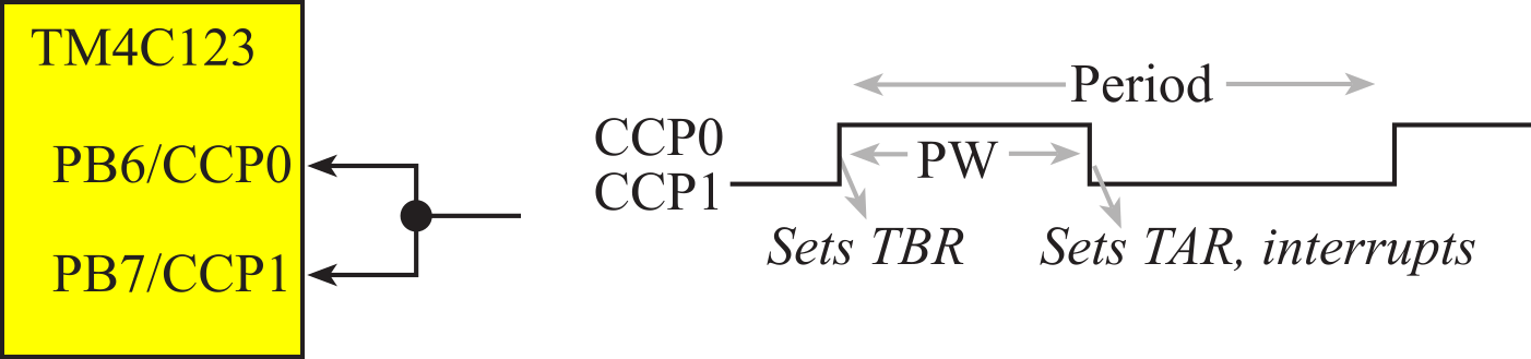
Figure T.9.3. The rising edge is measured with Timer0B, and falling edge is measured with Timer0A.
The pulse width measurement is performed from rising edge to falling edge. The resolution is 12.5 ns, determined by the system bus clock. The range is about 25 ns to 209ms with no overflow checking. Timer0A interrupts only occur on the falling edges. The global, PW, contains the most recent measurement. Done is set at the falling edge by the ISR signifying a new measurement is available. If the first edge after the PWMeasure2_Init(); is executed is a falling edge, then the first measurement will be incorrect (because TIMER0_TBR_R is incorrect). If the first edge after the PWMeasure2_Init(); is executed is a rising edge, then the first measurement will be correct. Notice how little software overhead is required to perform these measurements (Program T.9.1).
uint32_t PW; // 24 bits, 12.5 ns units
int Done; // set each falling
void PWMeasure2_Init(void){ // TM4C123 code
SYSCTL_RCGCTIMER_R |= 0x01; // activate timer0
SYSCTL_RCGCGPIO_R |= 0x02; // activate port B
Done = 0; // allow time to finish activating
GPIO_PORTB_DIR_R &= ~0xC0; // make PB6, PB7 inputs
GPIO_PORTB_DEN_R |= 0xC0; // enable digital PB6, PB7
GPIO_PORTB_AFSEL_R |= 0xC0; // enable alt funct on PB6, PB7
GPIO_PORTB_PCTL_R = (GPIO_PORTB_PCTL_R&0x00FFFFFF)+0x77000000;
TIMER0_CTL_R &= ~0x00000101; // disable timers 0A and 0B
TIMER0_CFG_R = 0x00000004; // configure for 16-bit timer mode
// **** timer0A initialization ****
TIMER0_TAMR_R = 0x00000007;
TIMER0_CTL_R = (TIMER0_CTL_R&(~0x0C))+0x04; // falling edge
TIMER0_TAILR_R = 0xFFFFFFFF; // start value
TIMER0_TAPR_R = 0xFF; // activate prescale, creating 24-bit
TIMER0_IMR_R |= 0x00000004; // enable capture match interrupt
TIMER0_ICR_R = 0x00000004; // clear timer0A capture match flag
// **** timer0B initialization ****
TIMER0_TBMR_R = 0x00000007;
TIMER0_CTL_R = (TIMER0_CTL_R&(~0x0C00))+0x00; // rising edge
TIMER0_TBILR_R = 0xFFFFFFFF; // start value
TIMER0_TBPR_R = 0xFF; // activate prescale, creating 24-bit
TIMER0_IMR_R &= ~0x0700; // disable all interrupts for timer0B
TIMER0_CTL_R |= 0x00000101; // enable timers 0A and 0B
// **** interrupt initialization ****
NVIC_PRI4_R = (NVIC_PRI4_R&0x00FFFFFF)|0x40000000; // Timer0=priority 2
NVIC_EN0_R = 1<<19; // enable interrupt 19 in NVIC
EnableInterrupts();
}
void Timer0A_Handler(void){
TIMER0_ICR_R = 0x00000004; // acknowledge timer0A capture flag
PW = (TIMER0_TBR_R-TIMER0_TAR_R)&0x00FFFFFF;// from rise to fall
Done = 1;
}
Program T.9.1. Pulse-width measurement using two input captures.
T.9.4. Resistance Measurement
We design a system to measure resistance and use it to interface a 10 kΩ joystick. See Figure T.9.4.
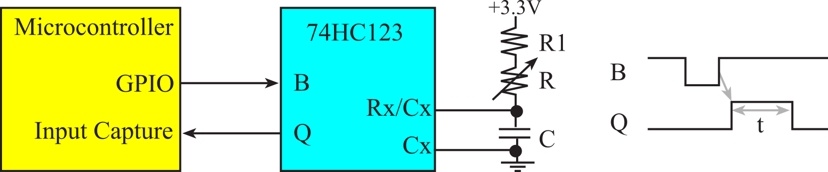
Figure T.9.4. To measure resistance using pulse width we connect the external signal an input capture.
The measurement function returns the resistance, R, in Ω. For example, if the resistance, R, is 1234 Ω, then the function will return 1234. We will not worry about resistances, R, greater than 55535 Ω or if R is disconnected. The solution is shown as Program T.9.2.
#define CALIBRATION 0
void ResistanceMeasure_Init(void){
SYSCTL_RCGCTIMER_R |= 0x01; // activate timer0
SYSCTL_RCGCGPIO_R |= 0x02; // activate port B
while((SYSCTL_PRGPIO_R&0x02) != 0x02){};
GPIO_PORTB_DATA_R |= 0x20; // set PB5 high
GPIO_PORTB_DIR_R = (GPIO_PORTB_DIR_R& ~0x40)|0x20; // PB5 out, PB6 in
GPIO_PORTB_DEN_R |= 0x60; // enable digital PB5 and PB6
GPIO_PORTB_AFSEL_R |= 0x40; // enable alt funct on PB6
GPIO_PORTB_PCTL_R = (GPIO_PORTB_PCTL_R&0xF0FFFFFF)+0x07000000;
TIMER0_CTL_R &= ~0x00000001; // disable timer0A during setup
TIMER0_CFG_R = 0x00000004; // configure for 16-bit timer mode
TIMER0_TAMR_R = 0x00000007; // configure for input capture mode
TIMER0_TAILR_R = 0xFFFFFFFF; // start value
TIMER0_IMR_R &= ~0x7; // disable all interrupts for timer0A
TIMER0_ICR_R = 0x00000004; // clear timer0A capture match flag
TIMER0_CTL_R |= 0x00000001; // enable timer0A edge, no interrupts
}
// return resistance in ohms, range is 0 to 10000 ohm
uint16_t ResistanceMeasure(void){ uint16_t rising;
GPIO_PORTB_DATA_R &= ~0x20; // turn off PB5
TIMER0_CTL_R &= ~(0x000C); // rising edge
TIMER0_ICR_R = 0x00000004; // clear timer0A capture flag
GPIO_PORTB_DATA_R |= 0x20; // turn on PB5, trigger 74HC123
while((TIMER0_RIS_R&0x00000004)==0){};// wait for rise
rising = TIMER0_TAR_R; // timerA0 at rising edge
TIMER0_ICR_R = 0x00000004; // clear timer0A flag
TIMER0_CTL_R &= ~(0x000C);
TIMER0_CTL_R += 0x00000004; // falling edge
while((TIMER0_RIS_R&0x00000004)==0){}; // wait for fall
TIMER0_ICR_R = 0x00000004; // clear timer0A flag
return(rising-TIMER0_TAR_R-CALIBRATION)&0xFFFF;
}
Program T.9.2. Measuring resistance using pulse-width measurement.
The difficulty with pulse width measurement in the previous example was the need to switch from rising to falling edge during each measurement. It was not a problem with this problem because the smallest pulse width was 125 µs. However, to handle shorter pulses we will need to use two input capture pins. One pin measures the time of the rise and the other pin measures the time of the fall. In order for input capture to operate, the input must be high for at least two bus clocks and low for at least two bus clocks. Otherwise, the minimum pulse width does not depend on software execution time or interrupt latency. However, the minimum period will depend on software speed.
We design an ohmmeter with a range of 0 to 250 kΩ and a resolution of 10Ω. One way to measure resistance or capacitance is convert the electrical parameter to time. In particular, we will use a TLC555 to convert the input resistance (Rin) to a time period (P) . Figure T.9.5 shows the hardware circuit. The 555 is called an astable multivibrator, created a signal wave with a period equal to CT*(RA + 2*RB)*ln(2). CT and RA are constants, but RB is 10kΩ plus the unknown input, Rin. We can then use the period measurement software from Program T.9.2. The resistance measurement resolution (ΔR) depends on the period measurement resolution (Δt) and the capacitor CT, Δt = CT *ΔR*ln(2). At a bus frequency of 50 MHz, the period measurement resolution is 20 ns. If we desire a 10Ω resistance resolution, the capacitor will be about 3nF. In this circuit, a 3.3nF capacitor was used because it is a standard value. As the input resistance varies from 0 to 250 kΩ, the period (in 20ns units) varies from about 3000 to 60000. A linear function is used to convert the measured period (20 ns units) to resistance (10Ω units). The same initialization of Program T.9.2 can be used.
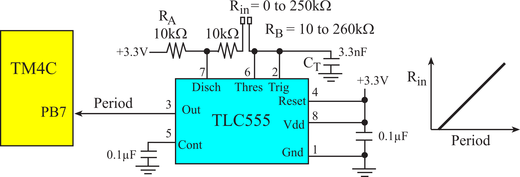
Figure T.9.5. The TLC555 outputs a square wave with a period depending on RA RB and CT.
Program T.9.3 shows the ISR extended to include the period to resistance conversion. The coefficients of this linear fit were determined by empirical calibration Rin = 0.4817*Period-1466.5. This equation is implemented with fixed-point math. Although mathematically, it seems like the system has a 10 Ω resolution and a precision of 25000 alternatives, the actual resolution will be limited by the stability of the TLC555, the stability of capacitor and any added noise into the circuit.
uint32_t Period; // 24-bit, 20 ns units
uint32_t Resistance; // 10 ohm units, 0 to 25000
uint32_t static First; // Timer0B first edge
uint32_t Done; // mailbox status set each rising
void Timer0B_Handler(void){
TIMER0_ICR_R = 0x00000400; // acknowledge timer0B capture
Period = (First - TIMER0_TBR_R)&0xFFFFFF; // 20 ns resolution
Resistance = (1973*Period-6006784)>>12; // conversion
First = TIMER0_TBR_R; // setup for next
Done = 1; // set mailbox flag
}
Program T.9.3. 24-bit period measurement is used to measure resistance.
T.9.5. Frequency Measurement
The direct measurement of frequency involves counting input pulses for a fixed amount of time. The basic idea is to use input capture to count pulses and use a periodic interrupt to create the fixed time interval, Δt. For example, we could initialize input capture to decrement a counter in TIMER0_TAR_R on every rising edge of our input signal. At the beginning of our fixed time interval, TIMER0_TAR_R is initialized to TIMER0_TAILR_R, and at the end of the interval, we can calculate frequency:
f = (TIMER0_TAILR_R - TIMER0_TAR_R)/Δt
The frequency resolution, ∆f, is defined to be the smallest change in frequency that can be reliably measured by the system. For the system to detect a change, the frequency must increase (or decrease) enough so that there is one more (or one less) pulse during the fixed time interval. Therefore, the frequency resolution is
∆f = 1/Δt
This frequency resolution also specifies the units of the measurement.
We design a system that measures frequency with a resolution of 100 Hz. If we count pulses in a 10ms time interval, then the number of pulses represents the signal frequency with units 1/10 ms or 100 Hz. E.g., if there are 7 pulses during the 10 ms interval then the frequency is 700 Hz. For this system, the measurement resolution is 100 Hz, so the frequency would have to increase to 800 Hz (or decrease to 600 Hz) for the change to be detected (Figure T.9.6.)
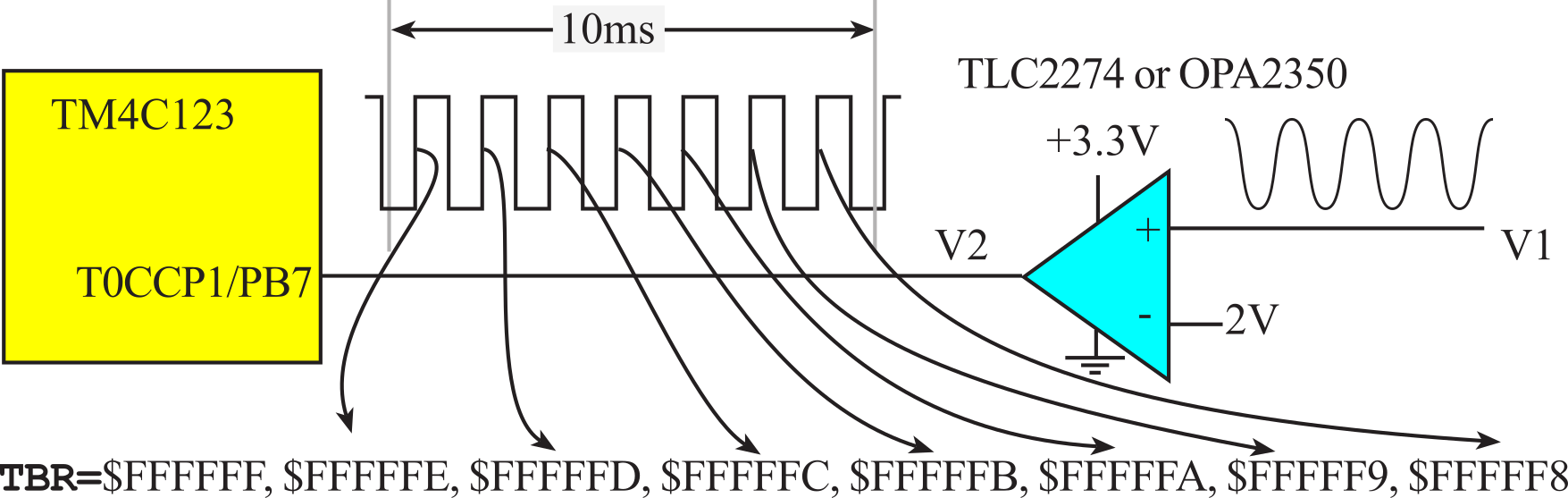
Figure T.9.6. Frequency measurement using both input capture and output compare.
The highest frequency that can be measured will be determined by how fast the Input Capture hardware can count pulses. Since there must be two clock periods while it is high and two clock pulses while it is low, the fastest frequency that can be measured is the bus frequency divided by four. The precision of the measurement is determined by the number of bits in the input capture register, which in this case is 16 bits. In this example, the digital logic input signal is connected to PB7 (T0CCP1, attached to Timer0B). The rising edge will decrement the counter in TIMER0_TBR_R.
The frequency measurement software is given as Program T.9.4. The frequency measurement counts the number of rising edges in a 10 ms interval. The measurement resolution is 100 Hz (determined by the 10 ms interval). A Timer0B input capture event occurs on each rising edge, and a Timer0A periodic interrupt occurs every 10 ms. The foreground/background threads communicate via a mailbox. The background thread will update the data in Freq with a new measurement and set the flag Done. When Done is set, the foreground thread will read the global Freq and clear Done.
uint32_t Freq; // Frequency with units of 100 Hz
int Done; // Set each measurement, every 10 ms
If the bus clock is 16 MHz, the largest frequency we can measure will be 8 MHz. Therefore, the maximum values of the frequency measurement will be 80000, which will not overflow the 24-bit counter. A frequency of 0 will result in no input capture events and the system will properly report the frequency of 0. The precision of this system is 80001 alternatives or about 16 bits.
void FreqMeasure_Init(void){
SYSCTL_RCGCTIMER_R |= 0x01; // activate timer0
SYSCTL_RCGCGPIO_R |= 0x02; // activate port B
Freq = 0; // allow time to finish activating
Done = 0;
GPIO_PORTB_DIR_R &= ~0x80; // make PB7 inputs
GPIO_PORTB_DEN_R |= 0x80; // enable digital PB7
GPIO_PORTB_AFSEL_R |= 0x80; // enable alt funct on PB7
GPIO_PORTB_PCTL_R = (GPIO_PORTB_PCTL_R&0x0FFFFFFF)+0x70000000;
TIMER0_CTL_R = 0x00000000; // disable TIMER0A TIMER0B during setup
TIMER0_CFG_R = 0x00000004; // configure for 16-bit mode
TIMER0_TAMR_R = 0x00000002; // TIMER0A for periodic mode
TIMER0_TAILR_R = 9999; // 4) reload value 100 Hz
TIMER0_TAPR_R = 15; // 1us resolution
TIMER0_TBMR_R = 0x00000003; // edge count mode rising edge on PB7
TIMER0_TBILR_R = 0xFFFFFFFF; // start value
TIMER0_TBPR_R = 0xFF; // activate prescale, creating 24-bit
TIMER0_IMR_R &= ~0x700; // disable all interrupts for timer0B
TIMER0_ICR_R = 0x00000001; // clear TIMER0A timeout flag
TIMER0_IMR_R = 0x00000001; // arm timeout interrupt
NVIC_PRI4_R = (NVIC_PRI4_R&0x00FFFFFF)|0x80000000; // priority 4
NVIC_EN0_R = 1<<19; // enable IRQ 19 in NVIC
TIMER0_CTL_R |= 0x00000101; // enable TIMER0A TIMER0B
}
// called every 10ms to collect a new measurement
void Timer0A_Handler(void){
TIMER0_ICR_R = 0x00000001; // acknowledge timer0A timeout
Freq = (0xFFFFFF-TIMER0_TBR_R); // f = (pulses)/(fixed time)
Done = -1;
TIMER0_CTL_R &= ~0x00000100; // disable TIMER0B
TIMER0_TBILR_R = 0xFFFFFFFF; // start value
TIMER0_TBPR_R = 0xFF; // activate prescale, creating 24-bit
TIMER0_CTL_R |= 0x00000100; // enable TIMER0B
}
Program T.9.4. Software to measure frequency with a resolution of 100 Hz.
T.9.5. Counting Wheel Rotations.
The initialization sets the direction register bit 6 to 0, so PB6 is an input. Bit 6 in GPIO_PORTB_AFSEL_R is set, making timer channel 4 an input capture. Bits 2 and 3 (TAEVENT) in TIMER0_CTL_R specify we want Timer0A to capture on the rising edge of PB6. We arm the input capture channel by setting bit 2 (CAEIM) in TIMER0_IMR_R. It is good design practice to clear trigger flags in the initialization, so the first interrupt is due to a rising edge on the input occurring after the initialization and not due to events occurring during power up or before initialization.
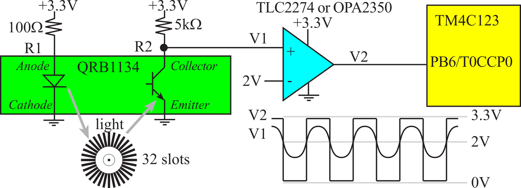
Figure T.9.7. An external signal is connected to the input capture.
volatile uint32_t Count; // incremented on interrupt
void TimerCapture_Init(void){
SYSCTL_RCGCTIMER_R |= 0x01; // activate timer0
SYSCTL_RCGCGPIO_R |= 0x00000002; // activate port B
Count = 0; // allow time to finish activating
GPIO_PORTB_DEN_R |= 0x40; // enable digital I/O on PB6
GPIO_PORTB_AFSEL_R |= 0x40; // enable alt funct on PB6
GPIO_PORTB_PCTL_R = (GPIO_PORTB_PCTL_R&0xF0FFFFFF)+0x07000000;
TIMER0_CTL_R &= ~0x00000001; // disable timer0A during setup
TIMER0_CFG_R = 0x00000004; // configure for 16-bit timer mode
TIMER0_TAMR_R = 0x00000007; // configure for input capture mode
TIMER0_CTL_R &= ~(0x000C); // TAEVENT is rising edge
TIMER0_TAILR_R = 0x0000FFFF; // start value
TIMER0_IMR_R |= 0x00000004; // enable capture match interrupt
TIMER0_ICR_R = 0x00000004; // clear timer0A capture flag
TIMER0_CTL_R |= 0x00000001; // enable timer0A
NVIC_PRI4_R =(NVIC_PRI4_R&0x00FFFFFF)|0x40000000; // Timer0A=priority 2
NVIC_EN0_R = 0x00080000; // enable interrupt 19 in NVIC
EnableInterrupts();
}
void Timer0A_Handler(void){
TIMER0_ICR_R = 0x00000004; // acknowledge timer0A capture match
Count = Count + 1;
}
Program T.9.5. Counting interrupt using input capture.
An input capture interrupt occurs on each rise of T0CCP0. The latency of the system is defined as the time delay between the rise of the input capture signal to the increment of Count. Assuming there are no other interrupts, and assuming the main program does not disable interrupts, the delay will be on the order of 1µs. The latency may be larger if there are other sections of code that execute with the interrupts disabled, or if there are higher priority interrupts active. The ritual, TimerCapture_Init(), sets input capture to interrupt on the rise, and initializes the global, Count. The interrupt software performs a poll, acknowledges the interrupt and increments the global variable. Actual measurements collected with this interface are shown in Figure T.9.8.
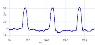
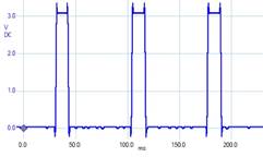
Figure T.9.8. Measured V1 and V2 from the circuit in Figure T.9.7.
On the TM4C123, the T0CCP0 input could be connected to either PB6 or to PF0 as described in Table T.4.1. We used PB6 so we set PCTL bits for PB6 to 7. To use PF0, we set PCTL bits for PF0 to 7. E.g.,
SYSCTL_RCGCGPIO_R |= 0x00000020; // activate port F
Count = 0;
GPIO_PORTF_DEN_R |= 0x01; // enable digital I/O on PF0
GPIO_PORTF_AFSEL_R |= 0x01;
GPIO_PORTF_PCTL_R = (GPIO_PORTF_PCTL_R&0xFFFFFFF0)+0x00000007;
: Explain how to change Program T.9.5 to still run on a TM4C123 with the input connected to T3CCP0/PB2.
: Write code to clear CBMRIS in Timer 1.
T.9.6. Using a tachometer to measure motor speed
We design a system that measures the rotational speed of a motor shaft using period measurement with a precision of 24 bits and a resolution of 12.5 ns. The Robot Systems Learning Kit has Hall effect sensors on ELA and ERA. In this example, we will measure the speed of the left motor using input capture. Each sensor has two outputs, A and B, which are 90 degrees out of phase. We could use B to determine the direction of rotation, but in this example the B signal will not be connected. Let N=360 be the number of rising edges as the shaft rotates once. We will make the bus clock equal 80 MHz. Each rising edge will generate an input capture interrupt (Figure T.9.9).
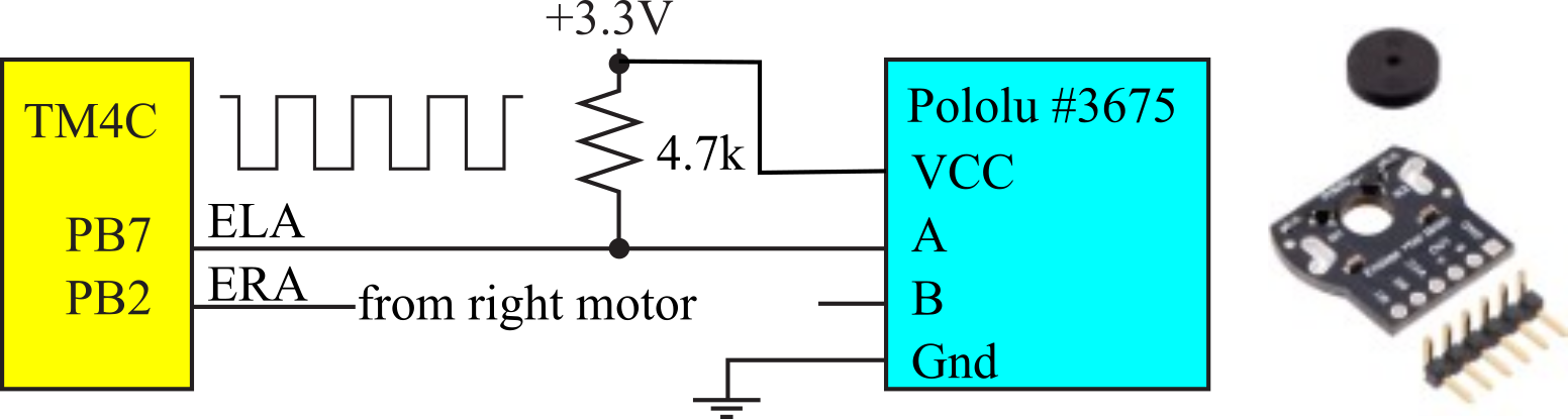
Figure T.9.9. To measure period we connect the external signal an input capture, PB7 on the TM4C123.
The period is calculated as the difference in TIMER0_TBR_R latch values from one rising edge to the other. If N=360, and the motor is spinning at 83.3 RPM, then the period will be [(60000ms/min)/(83.3RPM)/360edges/rotation)], which will be 2.00 ms/edge, see Figure T.9.10.
For example, if the period is 2000 µs, the Timer0B interrupts will be requested every 160,000 cycles, and the 24-bit difference between TIMER0_TBR_R latch values will be 160,000. This subtraction remains valid even if the timer reaches zero and wraps around in between Timer0A interrupts. On the other hand, this method will not operate properly if the period is larger than 224 cycles, or about 209 ms. 209 ms corresponds to a rotational speed of about 1 RPM.
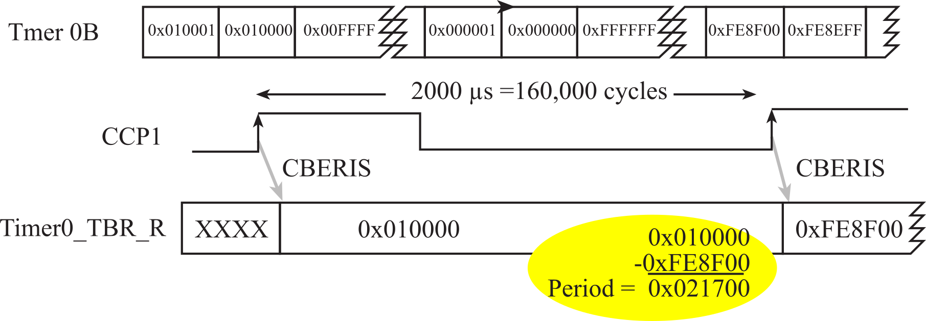
Figure T.9.10. Timing example showing counter rollover during 24-bit period measurement.
The resolution is 12.5 ns because the period must increase by at least this amount before the difference between Timer0B measurements will reliably change. Even though a 24-bit counter is used, the precision is a little less than 24 bits, because the shortest period that can be handled with this interrupt-driven approach is about 1 µs. It takes about 1 µs to complete the context switch, execute the ISR software, and return from interrupt. This factor is determined by experimental measurement. In other words, as the period approaches 1 µs, a higher and higher percentage of the computer execution is utilized just in the handler itself. For the RSLK robot the maximum speed is about 300 RPM, which corresponds to a period of about 500 µs.
Because the input capture interrupt has a separate vector the software does not poll. An interrupt is requested on each rising edge of the input signal. In this situation we count all the cycles required to process the interrupt. The period measurement system written for the TM4C123 is presented in Program T.9.6. The 24-bit subtraction is produced by anding the difference with 0x0FFFFFF, calculating the number of bus clocks between rising edges. The first period measurement will be incorrect and should be neglected.
uint32_t Period; // 24-bit, 12.5 ns units
uint32_t static First; // Timer0B first edge, 12.5 ns units
int32_t Done; // mailbox status set each rising
uint32_t Speed; // Speed, 0.1rpm
void PeriodMeasure_Init(void){
SYSCTL_RCGCTIMER_R |= 0x01; // activate timer0
SYSCTL_RCGCGPIO_R |= 0x02; // activate port B
First = 0; // first will be wrong
Done = 0; // set on subsequent
GPIO_PORTB_DIR_R &= ~0x80; // make PB7 input
GPIO_PORTB_AFSEL_R |= 0x80; // enable alt funct on PB7
GPIO_PORTB_DEN_R |= 0x80; // configure PB7 as T0CCP1
GPIO_PORTB_PCTL_R = (GPIO_PORTB_PCTL_R&0x0FFFFFFF)+0x70000000;
TIMER0_CTL_R &= ~0x00000100; // disable timer0B during setup
TIMER0_CFG_R = 0x00000004; // configure for 16-bit capture mode
TIMER0_TBMR_R = 0x00000007; // configure for rising edge event
TIMER0_CTL_R &= ~0x00000C00; // rising edge
TIMER0_TBILR_R = 0xFFFFFFFF; // start value
TIMER0_TBPR_R = 0xFF; // activate prescale, creating 24-bit
TIMER0_IMR_R |= 0x00000400; // enable capture match interrupt
TIMER0_ICR_R = 0x00000400; // clear timer0B capture match flag
TIMER0_CTL_R |= 0x00000100; // timer0B 24-b, +edge, interrupts
NVIC_PRI5_R = (NVIC_PRI5_R&0xFFFFFF00)|0x00000040; //Timer0B=priority 2
NVIC_EN0_R = 1<<20; // enable interrupt 20 in NVIC
EnableInterrupts();}
void Timer0B_Handler(void){
TIMER0_ICR_R = 0x00000400; // acknowledge timer0B capture
Period = (First - TIMER0_TBR_R)&0x00FFFFFF; // 12.5ns resolution
Speed = 133333333/ Period; // 0.1 RPM
First = TIMER0_TBR_R; // setup for next
Done = 1; // set semaphore
}
Program T.9.6. 24-bit period measurement.
T.10. Controller Area Network (CAN)
A device driver for the CAN network is divided into three components: initialization, transmission, and reception. There is a CAN driver available in TivaWare. In this section, we will use this driver to develop a simple system that exchanges 4-byte messages between two microcontrollers. Each node generates an interrupt when they receive a CAN message, and the interrupt handler dumps the data either into a mailbox. In this example, the transmission doesn't block, just returns a failure if it can't put, so it will not block or spin. This example was written using the TivaWare driverlib library. Figure T.10.1 shows the data flow. There are two IDs used in this example:
#define RCV_ID 2
#define XMT_ID 4
The CAN ID numbers must be reversed on the other microcontroller. Otherwise, the software functions on the two nodes are identical.
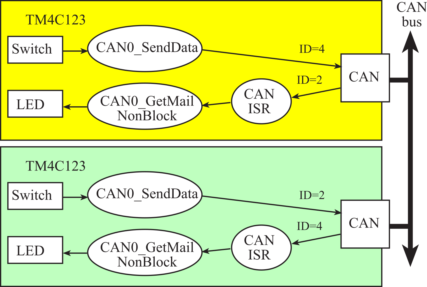
Figure T.10.1. Data flow for a simple CAN network.
Transmission uses busy-wait synchronization. However, receiving messages is interrupt driven, and data is passed from the ISR to the user application using a simple mailbox:
uint8_t static RCVData[4];
int static MailFlag; // set when new data arrives
The TM4C CAN receiver supports up to 32 message objects. Each message to be sent occupies a unique message object in the 32-object memory of the CAN controller and each receive object matches one of the transmit objects, just on the opposite board. Although this example has only two message objects it could easily be extended to up to 32 objects, but not beyond 32. In this code there are two message objects; the transmission object on one is connected to a receive object on the other. The following helper function sets up one of these 32 message objects, which can be a TX object or an RX object type.
void static CAN0_Setup_Message_Object( uint32_t MessageID,
uint32_t MessageFlags, uint32_t MessageLength,
uint8_t * MessageData, uint32_t ObjectID, tMsgObjType eMsgType){
tCANMsgObject xTempObject;
xTempObject.ulMsgID = MessageID; // 11 or 29 bit ID
xTempObject.ulMsgLen = MessageLength;
xTempObject.pucMsgData = MessageData;
xTempObject.ulFlags = MessageFlags;
CANMessageSet(CAN0_BASE, ObjectID, &xTempObject, eMsgType);
}
The initialization software first configures Port E bits 4,5 to be CAN0. From Table T.1.3, we see PE4 is CAN0Rx, and PE5 is CAN0Tx. Next, it initializes the baud rate to 1,000,000 bps. It arms CAN interrupts on error and status change. A status change will occur when an incoming frame is successively received. The CAN0_Setup_Message_Object function will configure one of the 32 message objects. Basically, it will set a filter to allow receive frames with this RCV_ID ID. An interrupt will be generated when receiving this type of frame, but other CAN traffic will be ignored. This function also specifies the expected size in bytes of the payload. Lastly, the CAN module is armed in the NVIC. Interrupts will be enabled in the main program after all devices are initialized.
void CAN0_Open(void){uint32_t volatile delay;
MailFlag = false;
SYSCTL_RCGCCAN_R |= 0x00000001; // CAN0 enable bit 0
SYSCTL_RCGCGPIO_R |= 0x00000010; // PortE enable bit 4
for(delay=0; delay<10; delay++){};
GPIO_PORTE_AFSEL_R |= 0x30; //PORTE AFSEL bits 5,4
GPIO_PORTE_PCTL_R = (GPIO_PORTE_PCTL_R&0xFF00FFFF)|0x00880000;
GPIO_PORTE_DEN_R |= 0x30;
GPIO_PORTE_DIR_R |= 0x20;
CANInit(CAN0_BASE);
CANBitRateSet(CAN0_BASE, 80000000, CAN_BITRATE);
CANEnable(CAN0_BASE);
CANIntEnable(CAN0_BASE,CAN_INT_MASTER|CAN_INT_ERROR|CAN_INT_STATUS);
CAN0_Setup_Message_Object(RCV_ID, MSG_OBJ_RX_INT_ENABLE, 4, NULL,
RCV_ID, MSG_OBJ_TYPE_RX);
NVIC_EN1_R = (1 << (INT_CAN0 - 48)); // IntEnable(INT_CAN0);
return;
}
Again, an interrupt is generated when a frame of the appropriate ID is received. The ISR will search the 32 possible message objects for the one that caused the interrupt.
void CAN0_Handler(void){uint8_t data[4]; int i;
uint32_t ulIntStatus,ulIDStatus; tCANMsgObject xTempMsgObject;
xTempMsgObject.pucMsgData = data;
ulIntStatus = CANIntStatus(CAN0_BASE, CAN_INT_STS_CAUSE); // cause?
if(ulIntStatus & CAN_INT_INTID_STATUS){ // receive?
ulIDStatus = CANStatusGet(CAN0_BASE, CAN_STS_NEWDAT);
for(i = 0; i < 32; i++){ // test every bit of the mask
if( (0x1 << i) & ulIDStatus){ // if active, get data
CANMessageGet(CAN0_BASE, (i+1), &xTempMsgObject, true);
if(xTempMsgObject.ulMsgID == RCV_ID){
RCVData[0] = data[0]; RCVData[1] = data[1];
RCVData[2] = data[2]; RCVData[3] = data[3];
MailFlag = true; // new mail
}
}
}
}
CANIntClear(CAN0_BASE, ulIntStatus); // acknowledge
}
When the user code wishes to receive a message, it calls CAN0_GetMailNonBlock, which is a simple mailbox receiver. This function is nonblocking, meaning if there is no message it returns false. If there is a message, it copies the payload of 4 bytes and returns true. If the RTOS were available, the MailFlag could be replaced with a semaphore. The ISR would signal the semaphore on new data, and the user code could wait on that semaphore.
int CAN0_GetMailNonBlock(uint8_t data[4]){
if(MailFlag){
data[0] = RCVData[0];
data[1] = RCVData[1];
data[2] = RCVData[2];
data[3] = RCVData[3];
MailFlag = false;
return true;
}
return false;
}
int CAN0_CheckMail(void){
return MailFlag;
}
When the user code wishes to transmit data it calls this function, which configures a new message object. This function will send 4 bytes of data to other microcontroller.
void CAN0_SendData(uint8_t data[4]){
CAN0_Setup_Message_Object(XMT_ID,NULL,4,data,XMT_ID,MSG_OBJ_TYPE_TX);
}
The UserTask ISR periodically reads its switches and creates a transmit object. Because the transmission rate is slower than the network, the transmitter does not wait. It simply creates the message object (CAN0_SendData) and schedules it for transmission. When received by the other microcontroller an interrupt is generated and the data is put in a mailbox. The main program on the other microcontroller reads the mail and writes the data out to its LED. Data flows in both directions. Remember to reverse the XMT_ID RCV_ID values on the two microcontrollers.
uint8_t XmtData[4];
uint8_t RcvData[4];
uint32_t RcvCount=0;
uint8_t sequenceNum=0;
void UserTask(void){
XmtData[0] = PF0<<1; // 0 or 2
XmtData[1] = PF4>>2; // 0 or 4
XmtData[2] = 0; // unassigned field
XmtData[3] = sequenceNum; // sequence count
CAN0_SendData(XmtData);
sequenceNum++;
}
int main(void){
PLL_Init(Bus80MHz); // bus clock at 80 MHz
SYSCTL_RCGCGPIO_R |= 0x20; // activate port F
while((SYSCTL_PRGPIO_R&0x20) == 0){};
GPIO_PORTF_LOCK_R = 0x4C4F434B; // unlock GPIO Port F
GPIO_PORTF_CR_R = 0xFF; // allow changes to PF4-0
GPIO_PORTF_DIR_R = 0x0E; // make PF3-1 output
GPIO_PORTF_AFSEL_R = 0; // disable alt funct
GPIO_PORTF_DEN_R = 0x1F; // enable digital I/O on PF4-0
GPIO_PORTF_PUR_R = 0x11; // enable pullup on inputs
GPIO_PORTF_PCTL_R = 0x00000000;
GPIO_PORTF_AMSEL_R = 0; // disable analog functionality on PF
CAN0_Open();
Timer3_Init(&UserTask, 1600000); // initialize timer3 (10 Hz)
EnableInterrupts();
while(1){
if(CAN0_GetMailNonBlock(RcvData)){
RcvCount++;
PF1 = RcvData[0];
PF2 = RcvData[1];
PF3 = RcvCount; // heartbeat
}
}
}
Program T.10.1. Very simple CAN network example.
In this simple example, there is just one transmit ID type and one receive ID type, but you could rewrite the transmitter and receiver to allow multiple ID types. In this case, the message ID (11-bit ID) and the object ID (0 to 31) are the same. In general, there could be 2048 IDs, but in this example only the first 32 can be used. The transmit messages are sent without interrupts, but the receive messages will trigger an interrupt. It would take three steps to expand to more receive IDs. First, we would call CAN0_Setup_Message_Object multiple times during initialization, once for each type of message we wish to receive (obviously, giving each a unique ID, up to 32). Second, for each possible ID, we would duplicate the if(xTempMsgObject.ulMsgID==RCV_ID){} test in the ISR to check if a desired message has been received. Third, each message ID would need its own mailbox or FIFO. This way the user tasks could be signaled when the appropriate data is available. Expanding the system to support more transmit message IDs is simple. We simple duplicate CAN0_SendData function for each message ID we wish to send.
This work is based on the course ECE445L
taught at the University of Texas at Austin. This course was developed by Jonathan Valvano, Mark McDermott, and Bill Bard.
Reprinted with approval from Embedded Systems: Real-Time Interfacing to ARM Cortex-M Microcontrollers, ISBN-13: 978-1463590154

Embedded Systems: Real-Time Interfacing to ARM Cortex-M Microcontrollers by Jonathan Valvano is
licensed under a Creative
Commons
Attribution-NonCommercial-NoDerivatives 4.0 International License.