5. Audio Processing
Table of Contents:
- 5.1. Fundamentals of Sound
- 5.2. Digital to Analog Converter Fundamentals
- 5.3. DAC Architectures
- 5.4. Interfacing
- 5.5. Approximating Continuous Signals in the Digital Domain
- 5.6. Lab 5. Audio Player
5.1. Fundamentals of Sound
 |
|
| Problems playing this file? See media help. | |
Before we generate sound, let's look
at the fundamentals of sound. Sound exists as varying pressure waves that are
created when a physical object moves, vibrating the air next to it.
These air pressure waves travel through the air in all directions at
about 343 m/sec. Sound can also be generated in water, where it travels
at 1484 m/sec. Our ears can sense sounds from 20 Hz to about 20 kHz. In
other words, the pressure wave must be oscillating faster than 20 Hz and
slower than 20 kHz for us to hear it. The wave equation as applied to sound is represented as:
∂2p/∂t2 = c2∇2p
where p represents the pressure variation in the medium, c is the speed of sound, t is time, and ∇2 is the Laplacian operator,
signifying the second spatial derivative in three dimensions;
essentially describing how pressure changes in a sound wave over time and space at a given point.
For a visualization of sound in one dimension, see Figure 5.1.1.
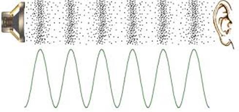
Figure 5.1.1. Sound waves exist as pressure waves in media such as air, water, and non-porous solids. For more information on sound, see http://www.mediacollege.com/audio/01/sound-waves.html
: Sound travels as a wave. Does the wave oscillate in time or in space?
There are two
magnets in a speaker. There is a large permanent magnetic that creates
a static magnetic field oriented in the direction the speaker is
facing, and there is a dynamic electromagnet created by a spiral-wound
coil oriented in the same direction. Figure 5.1.2 shows a magnetic
field generated by a cylindrically-wound coil.
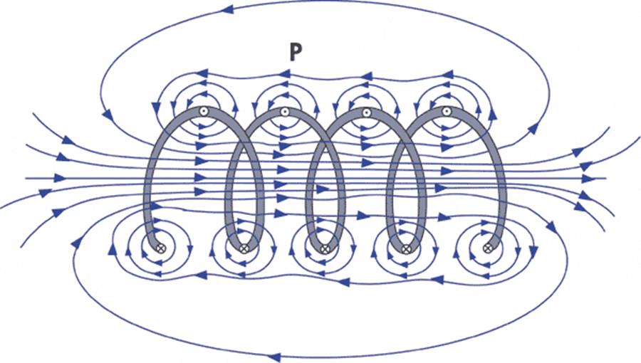
Figure 5.1.2. The magnetic field produced by a coil is very strong oriented in the direction of the cylinder. For more information on magnetic fields produced by a coil, see http://www.ndt-ed.org/EducationResources/CommunityCollege/MagParticle/Physics/CoilField.htm
The strength and direction of the magnetic field are related to the strength and direction of the electrical current conducted through the coiled wire. Figure 5.1.3 shows a cut away of a typical speaker. The alternating magnetic field generated by the coil interacts with the constant magnetic field produced by the permanent magnet. To generate sound we will create an oscillating current through the coil, this will create an oscillating magnetic field, and will vibrate the voice coil. The diaphragm and spider hold the voice coil to the suspension allowing it to vibrate up and down. Notice in the Figure 5.1.3, we want the diaphram to go both up and down. When the voice coil vibrates up and down it creates sound waves. The frequency and amplitude of the sound is directly related to the frequency and amplitude of the current passing through the coil. The resistance of the coil in a typical headphone is 32 Ω.
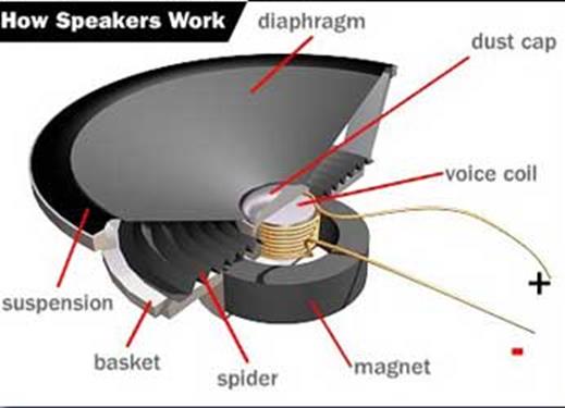
Figure 5.1.3. A speaker can generate sound by vibrating the voice coil using an electromagnet. For more information on speakers, see http://www.howstuffworks.com/speaker6.htm or http://www.audiocircuit.com/DIY/Dynamic-Speakers/Article:How-dynamic-loudspeakers-work
: Some speakers are heavier than others. These heavy speakers have larger permanent magnets. Why would we want a permanent magnet that can create a larger magnetic field?
Video 5.1.1. How the speaker works
Video 5.1.2. Sound as an analog signal: Loudness, pitch and shape
The quality of the music will depend on both hardware and software factors. The precision of the DAC, external noise, and the dynamic range of the speaker are some of the hardware factors. Software factors include the DAC output rate and the complexity of the stored sound data. If you output a sequence of numbers to the DAC that form a sine wave, then you will hear a continuous tone on the speaker, as shown in Figure 5.1.4. The loudness of the tone is determined by the amplitude of the wave. The pitch is defined as the frequency of the wave. Table 5.1.1 contains frequency values for the notes in one octave. The frequency of the wave, fsin, will be determined by the frequency of the interrupt, fint, divided by the size of the table n.
fsin = fint /n
The effective number of bits (ENOB)
of a sinewave generated by a DAC is limited by table size, n:
ENOB ≤ log2 n
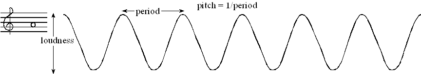
Figure 5.1.4. The loudness and pitch are controlled by the amplitude and frequency.
The frequency of each musical note can be
calculated by multiplying the previous frequency by![]() .
You can use this method to determine the frequencies of additional notes
above and below the ones in Table 5.1.1. There are twelve notes in an
octave, therefore moving up one octave doubles the frequency.
.
You can use this method to determine the frequencies of additional notes
above and below the ones in Table 5.1.1. There are twelve notes in an
octave, therefore moving up one octave doubles the frequency.
|
Note |
frequency |
|
C |
523 Hz |
|
B |
494 Hz |
|
Bb |
466 Hz |
|
A |
440 Hz |
|
Ab |
415 Hz |
|
G |
392 Hz |
|
Gb |
370 Hz |
|
F |
349 Hz |
|
E |
330 Hz |
|
Eb |
311 Hz |
|
D |
294 Hz |
|
Db |
277 Hz |
|
C |
262 Hz |
Table 5.1.1. Fundamental frequencies of standard musical notes. The frequency for ‘A’ is exact.
Figure 5.1.5 illustrates the concept of instrument. You can define the type of sound by the shape of the voltage versus time waveform. Brass instruments have a very large first harmonic frequency.
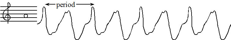
Figure 5.1.5. A waveform shape that generates a trumpet sound.
The tempo of the music defines the speed of the song. In 2/4 3/4 or 4/4 music, a beat is defined as a quarter note. A moderate tempo is 120 beats/min, which means a quarter note has a duration of ½ second. A sequence of notes can be separated by pauses (silences) so that each note is heard separately. The envelope of the note defines the amplitude versus time relationship. A very simple envelope is illustrated in Figure 5.1.6. The Cortex-M processor has plenty of processing power to create these types of waves.
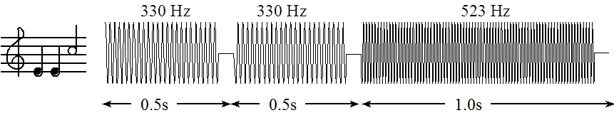
Figure 5.1.6. You can control the amplitude, frequency and duration of each note (not drawn to scale).
The smooth-shaped envelope, as illustrated in Figure 5.1.7, causes a less staccato and more melodic sound. This type of sound generation is possible to produce in real time on the Cortex™-M microcontroller.
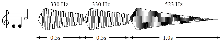
Figure 5.1.7. The amplitude of a plucked string drops exponentially in time.
A chord is created by playing multiple notes simultaneously. When two piano keys are struck simultaneously both notes are created, and the sounds are mixed arithmetically. You can create the same effect by adding two waves together in software, before sending the wave to the DAC. Figure 5.1.8 plots the mathematical addition of a 262 Hz (low C) and a 392 Hz sine wave (G), creating a simple chord.
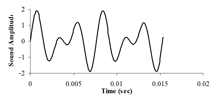
Figure 5.1.8. A simple chord mixing the notes C and G.
5.2. Digital to Analog Converter Fundamentals
A DAC converts digital signals into analog form as illustrated in Figure 5.2.1. Although one can interface a DAC to a regular output port, most DACs are interfaced using high-speed synchronous protocols. The DAC output can be current or voltage. Additional analog processing may be required to filter, amplify or modulate the signal. We can also use DACs to design variable gain or variable offset analog circuits.
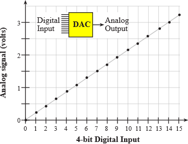
Figure 5.2.1. A 4-bit DAC converts digital inputs (0 to 15) into an analog output.
The DAC precision is the number of distinguishable DAC outputs (e.g., 16 alternatives, 4 bits). The DAC range is the maximum and minimum DAC output (e.g., 0 to 3.3V). The DAC resolution is the smallest distinguishable change in output. The resolution is the change in output that occurs when the digital input changes by 1 (e.g., 3.3V/15 = 0.22V). The units of range and resolution are in volts or amps depending on whether the output is voltage or current.
Range(volts) = Precision(alternatives) * Resolution(volts)
: What is the resolution of a 12-bit DAC with a range of 0 to 3.3V?
: Consider function call DAC_Out(n); to a 12-bit DAC with a range of 0 to 3.3V. If n=1000, what analog voltage would it create?
The DAC full-scale accuracy is (Actual - Ideal) / Maximum where Ideal is referred to the National Institute of Standards and Technology (NIST). One could choose the full-scale range of the DAC to simplify the use of fixed-point math. For example, if an 8-bit DAC had a full-scale range of 0 to 2.55 volts, then the resolution would be exactly 10 mV. This means that if the DAC digital input were 123 (decimal), then the DAC output voltage would be 1.23 volts.
A DAC gain error is a shift in the slope of the Vout versus digital input static response. A DAC offset error is a shift in the Vout versus digital input static response. The DAC transient response has three components: delay phase, slewing phase, ringing phase. During the delay phase, the input has changed but the output has not yet begun to change. During the slewing phase, the output changes rapidly. During the ringing phase, the output oscillates while it stabilizes. For purposes of linearity, let m, n be digital inputs, and let f(n) and f(m) be the analog outputs of the DAC, see Figure 5.2.2. One quantitative measure of linearity is the correlation coefficient of a linear regression fit of the f(n) responses. If ∆ is the DAC resolution, it is linear if
f(n+1)-f(n) = f(m+1)-f(m) = ∆ for all n, m
The DAC is monotonic if
sign(f(n+1)-f(n)) = sign(f(m+1)-f(m)) for all n, m
Conversely, the DAC is nonlinear if
f(n+1)-f(n) ≠ f(m+1)-f(m) for some n, m
Practically speaking all DACs are nonlinear, but the worst nonlinearity is nonmonotonicity. The DAC is nonmonotonic if
sign(f(n+1)-f(n)) ≠ sign(f(m+1)-f(m)) for some n, m
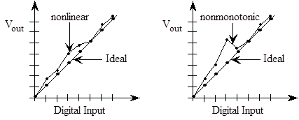
Figure 5.2.2. Nonlinear and nonmonotonic DACs.
Observation: In most applications, we are satisfied with a DAC if it is monotonic.
Many manufacturers, like Analog Devices, Texas Instruments, Maxim, Cirrus Logic, and Microchip Technology produce DACs. The MSPM0 family of microcontrollers have a 12-bit DAC built into the chip. For more information on the internal DAC of the MSPM0, see Appendix M.x (**add link). These DACs have a wide range of performance parameters and come in many configurations. The following paragraphs discuss the various issues to consider when selecting a DAC. Although we assume the DAC is used to generate an analog waveform, these considerations will generally apply to most DAC applications.
Precision/range/resolution. These three parameters affect the quality of the signal that can be generated by the system. The more bits in the DAC, the finer the control the system has over the waveform it creates. As important as this parameter is, it is one of the more difficult specifications to establish a priori. A simple experimental procedure to address this question is to design a prototype system with a very high precision (e.g., 12, 14, 16, or 20 bits.) The software can be modified to use only some of the available precision. For example, the 12-bit Max5353 interface is presented in Appendix T.5.2, can be reduced to 4, 8, or 10 bits using the following functions. The bottom bits are set to zero, instead of shifting so the rest of the system will operate without change.
void DAC_Out4(uint16_t code){
DAC_Out(code&0xFF00);} // ignore bottom 8 bits
void DAC_Out8(uint16_t code){
DAC_Out(code&0xFFF0);} // ignore bottom 4 bits
void DAC_Out10(unsigned int code){
DAC_Out(code&0xFFFC);} // ignore bottom 2 bits
Program 5.2.1. Software used to test how many bits are really needed.
Multiple versions of the software (e.g., 4-bit, 8-bit, 10-bit, and 12-bit DAC) are used to see experimentally the effect of DAC precision on the overall system performance. Figure 5.2.3 illustrates how DAC precision affects the quality of the generated waveform.
Figure 5.2.3. The waveform on the left uses a 4-bit DAC, while on one on the right uses a 12-bit DAC.
Channels. Even though multiple channels could be implemented using multiple DAC chips, it is more efficient to design a multiple channel system using a multiple channel DAC. Some advantages of using a DAC with more channels than originally conceived are future expansion, automated calibration, and automated testing. A multiple channel DAC allows you to update all channels at the same time.
Configuration. DACs can have voltage or current outputs. Current output DACs can be used in a wide spectrum of applications (e.g., adding gain and filtering), but do require external components. DACs can have internal or external references. An internal reference DAC is easier to use for standard digital input/analog output applications, but the external reference DAC can often be used in variable gain applications (multiplying DAC). Sometimes the DAC generates a unipolar output, while other times the DAC produces bipolar outputs.
Speed. There are a couple of parameters manufacturers use to specify the dynamic behavior of their DACs. The most common is settling time, another is the maximum output rate. When operating the DAC in variable gain mode, we are also interested in the gain/bandwidth product of the analog amplifier. When comparing specifications reported by different manufacturers it is important to consider the exact situation used to collect the parameter. In other words, one manufacturer may define settling time as the time to reach 0.1% of the final output after a full-scale change in input given a certain load on the output, while another manufacturer may define settling time as the time to reach 1% of the final output after a 1 volt change in input under a different load. The speed of the DAC together with the speed of the computer/software will determine the effective frequency components in the generated waveforms. Both the software (rate at which the software outputs new values to the DAC) and the DAC speed must be fast enough for the given application. In other words, if the software outputs new values to the DAC at a rate faster than the DAC can respond, then errors will occur. Figure 5.3.4 illustrates the effect of DAC output rate on the quality of the generated waveform. According to the Nyquist Theorem states the digital data rate must be greater than twice the maximum frequency component of the desired analog waveform. However, both waveforms in Figure 5.2.4 satisfy the Nyquist Theorem, but increasing the output rate by eight improves the signal to noise ratio by eight. 31 dB is a ratio of about 35 to 1, and 49 dB is a ratio of about 281 to 1. If the goal is to create a sine wave at a fixed frequency, we could improve the SNR greatly by using an analog low pass filter.
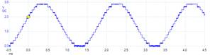

Experimental data of a 32-output 523 Hz sinewave Experimental data of a 256-output 523 Hz sinewave
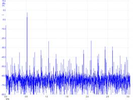
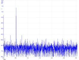
Signal/noise ratio is 31 dB (3dB — -28dB) Signal/noise ratio is 49 dB (3dB — -46dB)
Figure 5.2.4. The waveform on the right was created by a 12-bit DAC with eight times the output rate than the left. Voltage versus time data on top and the Fourier Transform (frequency spectrum dB versus kHz) of the data on the bottom. There is a point in the spectrum at 0, which is the DC component. However, the signal is the 523 Hz bump with a magnitude of 3dB, representing the sine wave. The noises are all the other points not at 0 or 523 Hz. The largest noise on the left is -28 dB. The largest noise on the right is -46 dB.
Most spectrum analyzers give the output in decibels full scale (dBFS). For a system with a range of 0 to 3.3V, the full scale peak-to-peak amplitude for any AC signal is 3.3 V. If V is the DFT output magnitude in volts
dBFS = 20 log10(V/3.3)
Since we are interested in the signal/noise ratio, the full scale value of 3.3V does not matter. Table 5.2.1 shows the mapping between dBFS and effective number of bits. We used the same table back in Section 2.4 (add link) when evaluating ADC resolution. For a real system, the resolution will be a function of other factors other than bits. In this case it is limited by the table size. The 12-bit DAC data collected in Figure 5.2.4 shows a signal/noise ratio of 49 dB, which is about 8 bits. Without an analog filter the effective number of bits in the sinewave was limited by the table size (ENOB ≈ log2 size).
|
Bits |
dBFS |
|
8 |
48.2 |
|
9 |
54.2 |
|
10 |
60.2 |
|
11 |
66.2 |
|
12 |
72.2 |
|
13 |
78.3 |
|
14 |
84.3 |
Table 5.2.1. ENOB for a DAC given SNR in dBFS.
Observation: Outputting at 133,888Hz to create a 523Hz wave is called oversampling.
Power. There are three power issues to consider. The first consideration is the type of power required. Older devices require three power voltages (e.g., +5 and -5 V), while most devices will operate on a single voltage supply (e.g., +2.7, +3.3, or +5 V.) If a single supply can be used to power all the digital and analog components then the overall system costs will be reduced. The second consideration is the amount of power required. Some devices can operate on less than 0.1 mW and are appropriate for battery-operated systems or for systems where excess heat is a problem. The last consideration is the need for a low-power sleep mode. Some battery-operated systems need the DAC only intermittently. In these applications, we wish to give a shutdown command to the DAC, so that it draws less current when not needed.
Interface. Two approaches exist for interfacing a DAC to the computer. In a digital logic or parallel interface, the individual data bits are connected to a dedicated computer output port. For example, a 6-bit DAC would requires 6 GPIO pins to interface. The software simply writes to the GPIO port to change the DAC output. The second approach is a high-speed serial interface like I2C or SPI. The TM4C123/MAX5353 interface is an example of a high-speed serial interface, see Appendix T.5.2. This approach requires the fewest number of I/O pins. Even if the microcontroller does not support the SPI interface directly, these devices can be interfaced to regular I/O pins via the bit-banging software approach.
Package. DIP packages are convenient for creating and testing an original prototype. On the other hand, surface mount packages require less board space. Because surface mount packages do not require holes in the PC board, circuits with these devices are easier to produce.
Cost. Cost is always a factor in engineering design. Besides the direct costs of the individual components in the DAC interface, other considerations that affect cost include: 1) power supply requirements; 2) manufacturing costs; 3) the labor involved in individual calibration if required; and 4) software development costs.
: In general, how does one choose the number of bits for a DAC?
Observation: The resolution of most DACs is limited by noise in the analog circuitry.
5.3. DAC Architectures
5.3.1. Binary-Weighted DAC
The first DAC architecture we will study is Binary Weighted. It is called binary weighted because the resistor values have a 1, 2, 4, 8, ... weighting. Figure 5.3.1 shows a 6-bit DAC built with E96 1% standard resistors. 1% error is of course 1 part out of 100. A 6-bit precision will be only 1 part out of 64. So, we expect it will be possible to build a 6-bit DAC with 1% parts. We begin the design by specifying the desired input/output relationship of the 6-bit DAC. All zeros will map to Vout=0, and all ones will map to Vout=3.3V. The exponential weighting of the bits corresponds to the basis elements in a 6-bit number. Let b5, b4, b3, b2, b1, b0 be the 6-bit DAC input, the desired performance is
Vout = 3.3V*(32*b5 + 16*b4 + 8*b3 + 4*b2 + 2*b1 + b0)/63
: Why does the equation divide by 63 instead of 64?
The circuit in Figure 5.3.1 uses E96 standard resistors approximating the desired exponential weighting. For more information on standard resistor capacitor values see Section 7.x( **add link**)
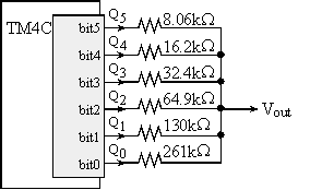
Figure 5.3.1. A 6-bit binary-weighted DAC, resistors are 1%.
The performance of the DAC is shown in Figure 5.3.2. This DAC remains monotonic even if the resistors are varied by ±1%.
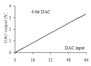
Figure 5.3.2. Performance of 6-bit binary-weighted DAC.
It is not feasible to construct a binary-weighted DAC with more than 8 bits for three reasons. First, if one chooses the resistor values from the practical 10kΩ to 1MΩ range, then the maximum precision would be 1MΩ/10kΩ, which equals 100 or about 7 bits. The second problem is that it would be difficult to avoid nonmonotonicity because a small percentage change in the small resistor (e.g., the one causing the largest gain) would overwhelm the effects of the large resistor (e.g., the one causing the smallest gain.) For example, if you tried to add a 7th bit to the DAC in Figure 5.3.1 using all 1% resistors, the DAC could become nonmonotonic. More specifically, when a 7-bit DAC goes from 0x3F to 0x40, all 7 bits are flipped. If the 8.06kΩ resistor is 1% higher (making 0x40 output lower), and the other six are 1% lower (making the 0x3F output higher), it will be non-monotonic. Third, the summing DAC includes the errors, uncertainty and noise because it it connected directly to the digital power supply. In particular, the GPIO output high voltage, VOH, is not exactly 3.3V, and the GPIO output low voltage, VOL, is not exactly 0V.
Observation: All DACs have something that is exponentially related to the number of bits. The resistor values of a binary-weighted DAC are exponentially related.
5.3.2. R-2R DAC
The second DAC architecture we will study is the R-2R Ladder. It is practical to build resistor networks such that all the resistances are equal. To create a 2R component, we use two resistors in series. Resistance errors due to manufacturing or temperature typically change all resistors equally. This type of error affects the slope, but not the linearity or the monotonicity of the DAC. In Figure 5.3.3, each of the three digital inputs (bit2, bit1, bit0) controls a transistor switch. When the digital signal is true, the reference current is injected to the ladder. When the digital signal is false, that position on the ladder is a virtual ground (0V). Using a reference voltage, shown as Vref, instead of the VOH of the microcontroller greatly reduces the noise in the output.
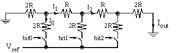
Figure 5.3.3. 3-bit unsigned R-2R DAC.
To analyze this circuit, we will consider the three basis elements (1, 2, and 4). If these three cases are demonstrated, then the law of superposition guarantees the other five will work. When one of the digital inputs is true then Vref is connected to the R-2R ladder, and when the digital input is false, then the connection is grounded. See Figure 5.3.4.
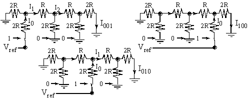
Figure 5.3.4. Analysis of the three basis elements {100, 010, 001} of the 3-bit unsigned R-2R DAC.
In each of the three test cases, the current across the active switch is I0=Vref/(3R). This current is divided by 2 at each branch point. I.e., I1 = I0/2, and I2 = I1/2. Current injected from the lower bits will be divided more times. Since each stage divides current by two, the exponential behavior is produced. An actual DAC is implemented with a current switch rather than a voltage switch. Nevertheless, this simple circuit illustrates the operation of the R-2R ladder function. When the input is 001, Vref is presented to the left. The effective impedance to ground is 3R, so the current injected into the R-2R ladder is I0=Vref/(3R). The current is divided in half three times, and I001=Vref/(24R).
When the input is 010, Vref is presented in the middle. The effective impedance to ground is still 3R, so the current injected into the R-2R ladder is I0=Vref/(3R). The current is divided in half twice, and I010=Vref/(12R).
When the input is 100, Vref is presented on the right. The effective impedance to ground is once again 3R, so the current injected into the R-2R ladder is I0=Vref/(3R). The current is divided in half once, and I100=Vref /(6R).
Using the Law of Superposition, the output voltage is a
linear combination of the three digital inputs,
Iout=(4b2
+ 2b1 + b0)Vref /(3R)
A current to voltage circuit is used to create a voltage output. To increase
the precision one simply adds more stages to the R-2R ladder.
: How would you design a 4 bit R-2R DAC?
Observation: All DACs have something that is exponentially related to the number of bits. Each stage of an R-2R ladder divides the current in half. The injection currents are all equal. So, the output current is exponentially related to the number of stages between injection and output.
5.3.3. Thermometer Coded/Resistor String DAC
The third DAC architecture we will present is Thermometer Coded or Resistor String. A 3-bit DAC is implemented with 8 equal-valued resistors, see Figure 5.3.5. The resistors create all the possible DAC output voltages. The transistors implement voltage-controlled switches. If the digital bit is high on the gate, that switch connects its drain to source. The line over the bit means complement, turning the switch on if the digital bit is low. This DAC is inherently monotonic because the resistors in series create voltages that increase from bottom to top. If the DAC has N bits, there will be 2N resistors and 2N+2N-1 +8+4+2 transistors, or 2N+1-1 transistors.
Figure 5.3.5. 3-bit Thermometer-coded DAC.
: What is the range, resolution, and precision of this 3-bit thermometer coded DAC?
: Why does the above equation divide by 8, rather than dividing by 7?
: How would you design a 4-bit thermometer coded DAC?
Observation: All DACs have something that is exponentially related to the number of bits. If N is the number of bits, the number of components in a thermometer coded DAC is related to 2N.
5.3.4. PWM DAC
The fourth architecture we will present is the PWM DAC. The PWM digital output is fed through an analog low-pass filter to create a DC voltage linearly related to the duty cycle of the PWM wave. The precision of the DAC will be the precision of the counter used to create the PWM. Details of the PWM module on the TM4C123 can be found in Appendix T.8. For example, if we call PWM_Init(4000,2000), then the DAC precision will be 4000 alternatives or about 12 bits. Alternatively, if we call PWM0_Init(250,125), then the DAC precision will be 250 alternatives or about 8 bits. The frequency of the DAC is the rate at which the DAC output can be changed and depends on the frequency of the PWM output. We can change the PWM duty cycle only once per cycle. If the PWM clock is 8 MHz, and we initialize with PWM0_Init(4000,2000), the PWM period will be 1ms. This means we can update the 12-bit DAC 1000 times a second. However, if the PWM clock were 50 MHz, and we initialize with PWM0_Init(250,125), the PWM period will be 10µs. This means we can update the 8-bit DAC 100,000 times a second. To change the analog output of the DAC we adjust the duty cycle of the PWM by calling
PWM0_SetDuty(duty);
where duty must be less than the period set by the call to PWM0_Init.
It is usually best for the PWM signal frequency to be 10 to 100 times higher than the desired bandwidth of analog signals to be produced. Generally, the higher the PWM frequency, the lower the order of filter required, and the easier it is to build a suitable filter. Let fmax be the highest frequency component we wish to create in the analog output, and let fPWM be the PWM frequency. We want the analog LPF to reject fPWM and pass fmax.
PWM DACs are very inexpensive. Figure 5.3.6 shows a DAC built with one resistor and one capacitor. We will output to this DAC at a rate less than 100 kHz, creating signals less than 1 kHz. The LPF must pass 1 kHz and reject 100 kHz. We chose the LPF cutoff at 3 kHz, which is between fPWM and fmax. A passive LPF can be made with a resistor and capacitor, fc = 1/(2πRC). An R equal to 22 kΩ and C equal to 2.2nF will create a LPF at 3.3 kHz. If we need low output impedance, we could add an analog buffer (see Section 6.xx) or an active analog filter (see Section 6.yy)
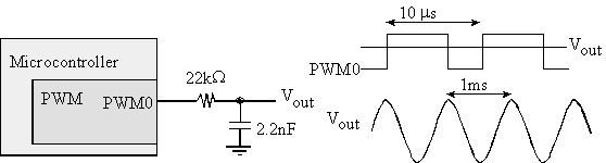
Figure 5.3.6. PWM DAC used to create a 1 kHz sine wave.
: Assuming we initialize the PWM with PWM0_Init(1000,125), what is the range, resolution, and precision of this PWM DAC?
Observation: All DACs have something that is exponentially related to the number of bits. If N is the number of bits, the number of different duty cycles is 2N.
5.4. Interfacing
5.4.1. Microphone Interface
The electret microphone was described previously in
Section 2.2.5 as a low-cost, small-size
transducer capable of converting sound into voltage. Many electret data sheets
suggest powering the microphone with of 2 kΩ, but signal-to-noise ratio may be improved by
replacing the two 1kΩ resistors with two 4.7kΩ resistors.
Because the output of a HPF would normally include
positive and negative voltages, we will need a way to offset the circuit so all
voltages exist from 0 to +3.3 V, allowing the use of a single supply and
rail-to-rail op amps. R2 and R3 provide an offset for the HPF, so
the signal V2 will be the sound signal plus 1.65 V. The effective
impedance from V2 to ground is 50 kΩ, so the HPF cutoff is 1/(2π*0.1µF*50kΩ)
= 32 Hz. The gain of the system is 1+R6/R5, which will be 101.
The capacitor C2 will make the signal V3 be the amplified sound
plus 1.65 V. The gain is selected so the V3 signal is 1.65 ±1 V for the
sounds we wish to record. The capacitor C3 provides a little low pass
filtering, causing the amplifier gain to drop to one for frequencies above 1/(2π*100pF*100kΩ)
= 16 kHz. If we wish to process sound with frequency components from 100 to 5
kHz, then we should sample at or above 10 kHz.
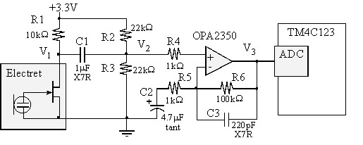
Figure 5.4.1. An electret microphone can be used to record sound.
: Why does the microphone amp have a high-pass filter with C1 and C2?
: How does one calculate the DC response of this circuit?
: How does one calculate the response of this circuit for frequencies from 100 to 10 kHz?
: How does one calculate the response of this circuit for frequencies above 100 kHz?
One of the problems with inexpensive microphones is when the sound amplitude is low (i.e., it is quiet), the noise can be very large (see Figure 5.4.2). The noise originates in the microphone, it is random, independent identically distributed, and not correlated to itself. The sound signal in contrast comes from sound pressure and is highly correlated to itself.
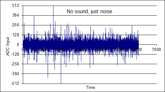
Figure 5.4.2. The electret is very noisy when there is no sound.
This correlated/not-correlated property is the theory behind a widely used adaptive noise reduction digital filter used with microphones:
http://www.ti.com/lit/an/spra657/spra657.pdf
The definition of auto correlation is

where Rxx(m) will be large if x is the same shape as itself, shifted m points. It is a digital filter, so the data has been sampled at fs, meaning the time between samples is Δt=1/ fs. To use the above equation, we guarantee x(n) has zero mean. I.e., it is just the shape with the DC component removed. To make it run in real time, we will pick one value for m, e.g., m=2. Rather than do an infinite sum, we can approximate the infinite behavior with a recursive relationship. The constant K is called the attack ratio, and it determines how fast the output changes in response to changes in input sound.

Many integrated microphone systems have this noise-reducing filter implemented in analog hardware.
The variables t0, t1, t2 implement a MACQ, see Section 2.6.1. Rxx2 will vary from 0, to K. The filter gain is Rxx2/K. Rxx2/K=0, means uncorrelated, and Rxx2/K=1 means very correlated. The two if statements guarantee the gain will always be less than or equal to 1.
int32_t t0,t1,t2; // last 3 inputs/32
int32_t Rxx2; // autocorrelation factor
#define K 128 // how fast it responds
#define M 128 // gain bound
int32_t NoiseReject(int32_t x){
t2 = t1;
t1 = t0;
t0 = x/32;
Rxx2 = ((K-1)*Rxx2 + t0*t2)/K;
if(Rxx2 < -M) Rxx2 = -M;
if(Rxx2 > M) Rxx2 = M;
return (Rxx2*x)/K;
}
Program 5.4.1. Adaptive noise
reducing digital filter.
Observation: We use signed data types when processing sound.
Typical sound data is presented in Figures 5.4.3 and 5.4.4. The blue traces are input data x(n) and the orange traces are the filter output using Program 5.4.1. Figure 5.4.3 is when there is no sound, showing the filter completely removes the noise. Figure 5.4.4 is when there is a single frequency tone, showing the filter passes the sound exactly (you do not see the orange trace because it is exactly under the blue trace.
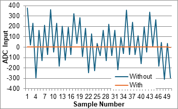
Figure 5.4.3. Filter response when there is no sound.
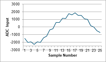
Figure 5.4.4. Filter response in the presence of sound.
The ADC fundamentals can be found in Section 2.3. Low-level ADC software can be found in Appendix T.2. Periodic timer software is presented in Appendix T.3. The FIFO was presented in Section 2.7. Data are put into a FIFO to be processed later.
void SampleSound(void){ int32_t x,y;
Debug_HeartBeat0();
x = ADC_In() - 2048; // sound, -2048 to +2047
y = NoiseReject(x); // filter, record etc.
Fifo_Put(y); // producer thread
Debug_HeartBeat0();
}
#define F11KHZ (80000000/11000)
void main(void){
PLL_Init(); // 80 MHz TM4C123
ADC_Init(); // sample at 10 kHz
Debug_Init(); // Section T.1
Timer_Init(&SampleSound, F11KHZ,2); // 11kHz
EnableInterrupts();
while(1){
// get from FIFO and process
}
}
Program 5.4.2. Real-time sound input.
: How do you use the debugging instruments Debug_HeartBeat0() to measure the percentage of time needed to run the ISR?
5.4.2. Speaker Interface
A class AB amplifier is a type of amplifier class commonly used in audio systems. In a Class AB amplifier, the output transistors operate in pairs, where one handles the positive half of the input waveform, and the other handles the negative half. Class AB amplifiers have each transistor conducting only for a portion of the input signal cycle. The key characteristics of Class AB amplifiers include (https://www.cytechsystems.com/news/class-ab-vs-class-d-amplifier):
Efficiency: Class AB amplifiers are more efficient than Class A amplifiers because they only conduct for a portion of the input signal cycle. However, they are less efficient than Class D amplifiers. Typically, Class AB amplifiers have efficiency ratings ranging from 50% to 78%.
Linearity: They provide good linearity, meaning they can accurately reproduce the input signal without significant distortion. This makes Class AB amplifiers suitable for audio applications where fidelity is important.
Power Dissipation: While more efficient than Class A amplifiers, Class AB amplifiers still dissipate a significant amount of power as heat, especially when operating at higher power levels. Heat sinks are often used to dissipate this heat and prevent damage to the amplifier components.
Audio Quality: Class AB amplifiers are known for their excellent audio quality, with low distortion and good signal fidelity. They are commonly used in high-fidelity audio systems, professional audio equipment, and other applications where audio quality is paramount.
Observation: Class AB amplifiers strike a balance between efficiency and audio quality, making them a popular choice for a wide range of audio applications.
A class D amplifier is known for its high efficiency and compact size. Class D amplifiers employ a switching process to amplify signals digitally. The input audio signal is converted into a series of pulses, typically by using pulse-width modulation (PWM). These pulses are then amplified using high-speed switching transistors, usually MOSFETs, which rapidly switch on and off to reproduce the audio waveform. The TPA3250 is a 70 W stereo class D audio amplifier, operating on a supply voltage of 12 to 38V, and it can drive two 8-Ω speakers. Key characteristics of Class D amplifiers include (https://www.cytechsystems.com/news/class-ab-vs-class-d-amplifier):
Efficiency: Class D amplifiers are highly efficient, often achieving efficiency ratings above 90%. This high efficiency means they waste less power as heat compared to traditional analog amplifiers, making them suitable for battery-powered devices and applications where power efficiency is critical.
Size and Weight: Due to their high efficiency and reduced heat dissipation, Class D amplifiers can be much smaller and lighter than traditional analog amplifiers. This makes them ideal for compact designs and portable devices such as smartphones, portable speakers, and car audio systems.
Linearity: While early Class D amplifiers faced challenges in achieving the same level of linearity as traditional analog amplifiers, modern designs have significantly improved. Advanced feedback and filtering techniques are used to minimize distortion and ensure accurate signal reproduction.
Audio Quality: Initially criticized for lower audio quality compared to traditional analog amplifiers, modern Class D designs have greatly improved, offering comparable audio performance in many cases. Class D amplifiers are now commonly used in high-quality audio systems and professional audio equipment.
Observation: Class D amplifiers offer a combination of high efficiency, compact size, and improved audio quality, making them well-suited for a wide range of audio applications, particularly those requiring portable or energy-efficient solutions.
Figure 5.4.5 shows a simple circuit that takes a DAC output and drives a speaker. The details of the MAX5353 DAC interface to the microcontroller was presented in Appendix T.5.2. The TPA731 is a class AB audio amp, and can be used to amplify the DAC output providing the current needed to drive a typical 8-Ω speaker. The gain of the audio amplifier is 2*R11/R10, which for this circuit will be one. This means a 2-V peak-to-peak signal out of the DAC will translate to a 2-V peak-to-peak signal on the speaker. The maximum power that the TPA731 can deliver to the speaker is 700 mW, so the software should limit the sound signal below 2.3 Vrms when driving an 8-Ω speaker. The quality of sound can be increased by selecting a better speaker and placing the speaker into an enclosure. For more information on how to design a speaker box, perform a web search on "speaker enclosure design".
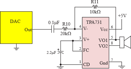
Figure 5.4.5. A 12-bit DAC and a class AB audio amplifier allow the microcontroller to output sound.
: What is the purpose of the 0.1uF and 2.2uF capacitors?
Pins 5 and 8 contain the sound signal, but these two signals will be 180 degrees out of phase. The AC voltage difference drives sound to the speaker, as shown in Figure 5.4.6. The DC voltage across the speaker will be of 0.
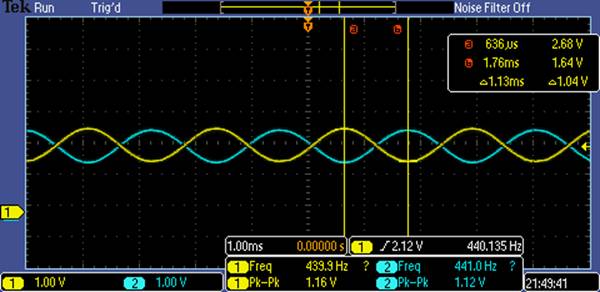
Figure 5.4.6. Two channel recording of pins 5 and 8. DC component is 2.12V, peak to peak is 1.16V (amplitude of the sound), and the frequency is 440 Hz.
Observation: There are two advantages of the audio amp over a regular op amp. First, the voltage maximum difference across the speaker is -5 to +5V volts (rather than 0 to 5V). Second, the DC voltage on the speaker is 0, meaning the electromagnet in the speaker both pushes in and pulls out (rather than just one direction). This gives a much richer sound.
5.4.3. DAC Interface
The MSPM0G3507 has an internal 12-bit DAC (see Appendix M.x). However, for most microcontrollers, we will interface an external DAC to microcontroller, using a serial protocol like SPI. Figure 5.4.7 shows an interface to a 12-bit thermometer-coded DAC, TLV5616. The low-level software for a similar interface (MAX5353) is presented in Appendix T.5.2. With a reference voltage of 1.225V the range of this 12-bit DAC will be 0 to 2.45V.
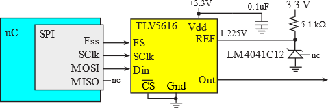
Figure 5.4.7. An external DAC interfaced with SPI.
Figure 5.4.8 shows the TLV5616 timing. The SPI is configured in 16-bit, SPO=1, SPH=0, and 10 MHz clock. The microcontroller shifts data out on rising edge, while the DAC shifts data in on falling edge. 16 bits are sent in one frame. Bits 15 and 12 are not used. Bit 14 sets the speed; SPD=1 is fast and noisy, while SPD=0 is slow and less noisy. Bit 13 is PWR, where PWR=1 will power down the DAC, and PWR=0 will make the DAC operate normally. Bits 11-0 are the digital data.
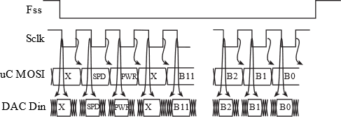
Figure 5.4.8. TLV5616 DAC timing, using SPO=1 SPH=0 SPI mode.
: What makes SPI so fast?
: When would one set PWR=1?
5.5. Approximating Continuous Signals in the Digital Domain
An analog signal is one that is continuous in both amplitude and time. Neglecting quantum physics, most signals in the world are continuous in time and continous in amplitude (e.g., voltage, current, position, angle, speed, force, pressure, temperature, and flow etc.) In other words, the signal has amplitude that can vary over time, but the value cannot instantaneously change. To represent a signal in the digital domain we must approximate it in two ways: amplitude quantizing and time quantizing (called sampling). From an amplitude perspective, we will first place limits on the signal restricting it to exist between a minimum and maximum value (e.g., 0 to 15 mm), and second, we will divide this amplitude range into a finite set of discrete values. The range of the system is the maximum minus the minimum value. The precision of the system defines the number of values from which the amplitude of the digital signal is selected. Precision can be given in number of alternatives, binary bits, or decimal digits. The resolution is the smallest change in value that is significant. Furthermore, with respect to time, one considers analog signals to exist from time equals minus infinity to plus infinity. Because memory is finite, when representing signals on a digital computer, we will restrict a signal to a finite time. This means a finite number of data points are stored in one finite-sized array. To model this finite data as having infinite time, we consider the situation where the data is repeated over and over.
Figure 5.5.1 shows a position waveform (solid line), with a corresponding digital representation sampled at 1 Hz and stored as a 4-bit integer number with a range of 0 to 15 mm. Because it is digitized in both amplitude and time, the digital samples (individual dots) in Figure 5.5.1 must exist at an intersection of grey lines. Because it is a time-varying signal (mathematically, this is called a function), we have one amplitude for each time.
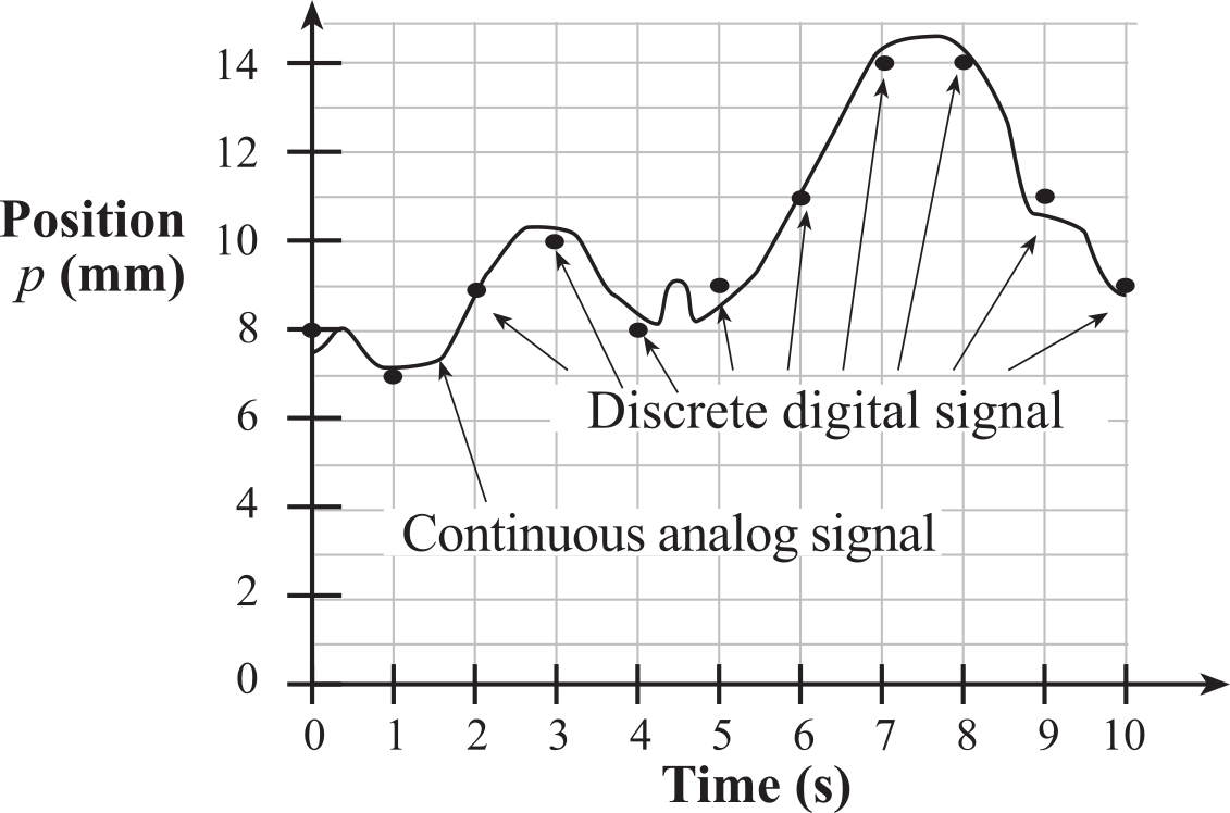
Figure 5.5.1. A continuous analog signal is represented in the digital domain as discrete samples
Video 5.5.1. Fundamentals of Digitization
The second approximation occurs in the time domain. Time quantizing is caused by the finite sampling interval. For example, the data are sampled every 1 second in Figure 5.5.1. To have an accurate time base we will use a periodic timer to trigger an analog to digital converter (ADC) to digitize information, converting from the analog to the digital domain. Similarly, if we are converting from the digital to the analog domain, we use the periodic timer to output new data to a digital to analog converter (DAC).
The Nyquist Theorem states
that if the signal is sampled with a frequency of fs,
then the digital samples only contain frequency components from 0 to
½ fs. Conversely, if the analog signal does
contain frequency components larger than ½ fs,
then there will be an aliasing error during the sampling
process. Aliasing
is when the digital signal appears to have a different frequency than
the original analog signal. Also note, the digital data has 11 values from
times 0 to 10, but no information before time=0, and no information
after time=10. This finite time results in a limitation called frequency resolution.
Frequency resolution, Δf, is the smallest difference in frequency we can represent.
If
fs is the sampling rate, and the N is the size
of the finite buffer holding the digital data, the total sampling time is
T = N/fs
and the frequency resolution is
Δf = fs/N = 1/T
: Why can't the digital samples represent the little wiggles in Figure 5.5.1?
: Why can't the digital samples represent distance above 15 mm in Figure 5.5.1?
: What range of frequencies is represented in the analog output when the DAC is output once every millisecond?
: If I wanted to create an analog output wave with frequencies 0, 1, 2, ... to 100Hz, with a sampling rate of 1 kHz, how size buffer do I need?
Discover the Nyquist Theorem. A continuous waveform is shown, V = 1.5 + 1*sin(2π 50t)+0.5*cos(2π 200t). You may select the sampling rate and the precision (in bits) to see the signal generated by a periodic output of the DAC. Notice that at sampling rates above 100 Hz you capture the essence of the 50Hz periodic wave, and above 400 Hz you capture the essence of both the 50 and 200 Hz waves. To "capture the essence" means the analog and digital signal go up and down at the same rate.
Number of DAC bits = bit(s)
Observation: Since the wave frequencies in Interactive Tool 5.5.1 are fixed at 50 and 200 Hz, increasing the sampling rate is the same as increasing the size of the data buffer.
: At what sampling frequencies can we see the wiggles of the 200 Hz component?
: Can I improve the quality of the DAC output by just increasing sampling rate?
Next, we will discuss various software methods for creating analog waveforms with a DAC. In each case, we will be using a 12-bit DAC. In addition, we will use periodic interrupt for the timing, so that the waveform generation occurs in the background. For details on periodic interrupts, refer to Appendix T.3. To get a fair comparison between the various methods, each implementation will generate 32 interrupts per waveform.
In the first approach, we assume there exists a time to voltage function, called Wave(), which we can call to determine the next DAC value to output. The waveform on the left of Figure 5.5.2 could be generated by Program 5.5.1. A periodic interrupt occurs every 1/fs = 1 ms. The advantage of this approach is that complex waveforms can be encoded with a small amount of data. In this example, the entire waveform can be stored as 5 data points (2048.0 1000.0 31.25 -500.0 125.0). The disadvantage of this technique is that not all waveforms have a simple function, and this software will run slower as compared to the other techniques. If you were to implement this approach, speed would be improved by replacing the floating-point with fixed-point.
float Time; // incremented every 1ms
const float A=2048.0, B=1000.0, C=2*pi*31.25, D=-500.0, E=2*pi*125.0;
uint16_t Wave(float time){ float result;
result = A + B*cos(C*time) + D*sin(E*time);
return (uint16_t) result;
}
void OutputDAC1(void){ int32_t x,y;
Debug_HeartBeat0();
Time = Time+0.001;
DACout(Wave(Time));
Debug_HeartBeat0();
}
#define F1KHZ (80000000/1000)
void main(void){
PLL_Init(); // 80 MHz TM4C123
DAC_Init();
Debug_Init(); // Section T.1
Timer_Init(&OutputDAC1, F1KHZ,2); // 1kHz
EnableInterrupts();
while(1){
Debug_HeartBeat1();
}
}
Program 5.5.1. Analog waveform created with a floating-point function.
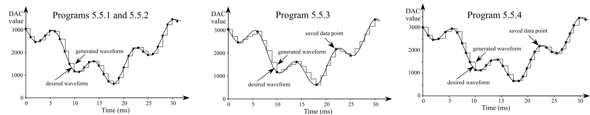
Figure 5.5.2. Generated waveforms. Left uses either the floating-point function (Program 5.5.1) or the table lookup technique (Program 5.5.2). Center uses a small table and interpolation (Program 5.5.3). Right uses a variable output rate (Program 5.5.4).
In the second approach, we put the waveform information in a large statically allocated global array, see Program 5.5.2. Every interrupt we fetch a new value out of the data structure and output it to the DAC. In this case the periodic interrupt also occurs at a regular rate. Assume the ritual initializes Time=0. Running at 80 MHz, the ISR in Program 8.4 executes in less than 1 µs.
uint16_t Time; // incremented every 1ms, 0-31
const uint16_t Wave[32]= { 3048,2675,2472,2526,2755,2957,
2931,2597,2048,1499,1165,1139,1341,1570,1624,1421,1048,714,624,863,
1341,1846,2165,2206,2048,1890,1931,2250,2755,3233,3472,3382
};
uint16_t Time; // every 1ms
void OutputDAC2(void){
Debug_HeartBeat0();
Time = (Time+1)&0x1F;
DACout(Wave[Time]));
Debug_HeartBeat0();
}
#define F1KHZ (80000000/1000)
void main(void){
PLL_Init(); // 80 MHz TM4C123
DAC_Init();
Debug_Init(); // Section T.1
Timer_Init(&OutputDAC2, F1KHZ,2); // 1kHz
EnableInterrupts();
while(1){
Debug_HeartBeat1();
}
}
Program 5.5.2. Analog waveform created with large integer array.
Since the output rate is equal and fixed for Programs 5.5.1 and 5.5.2, they will have the same output wave as illustrated on the left of Figure 5.5.2. The smooth line is the desired waveform, and the blocky line is the actual generated curve.
If the size of the table gets large it is possible to store a smaller table in memory and use linear interpolation to recover the data points between the stored samples. The center of Figure 5.5.2 shows the generated waveform derived from only 9 of the original 32 data points. To simplify the software, the first data point is repeated as the last data point. For each point we will need to save both the DAC value and time length of the current line segment. For the 9 saved data points we simply output the data, but for the other points, we must perform a linear interpolation to get the value to output to the DAC, see Program 5.5.3. Assume the ritual initializes I=J=0. Signed 16-bit numbers are used so the subtractions operate properly. In other words, some of the intermediate calculations can be negative.
int16_t I; // incremented every 1ms
int16_t J; // index into these two tables
const int16_t Time[10]= {0,2,6,10,14,18,22,25,30,32}; // time in msec
const int16_t Wave[10]=
{3048,2472,2931,1165,1624,624,2165,1890,3472,3048}; // last=first
uint16_t Time; // every 1ms
void OutputDAC3(void){
Debug_HeartBeat0();
if((++I)==32) {I=0; J=0;}
if(I==Time[J]){
DACout(Wave[J]);
}
else if (I==Time[J+1]){
J++;
DACout(Wave[J]);
}
else{
DACout(Wave[J]+((Wave[J+1]-Wave[J])*(I-t[J]))/(Time[J+1]-Time[J]));
}
Debug_HeartBeat0();
}
#define F1KHZ (80000000/1000)
void main(void){
PLL_Init(); // 80 MHz TM4C123
DAC_Init();
Debug_Init(); // Section T.1
Timer_Init(&OutputDAC3, F1KHZ,2); // 1kHz
EnableInterrupts();
while(1){
Debug_HeartBeat1();
}
}
Program 5.5.3. Analog waveform created with two small integer arrays and interpolation.
: Why does Program 5.5.3 use signed data types when all the data are unsigned?
The software in the previous techniques changes the DAC at a fixed rate. While most of the time this is adequate, there are some waveforms for which uneven times between outputs seem appropriate. In our test signal, there are places in the wave where the signal varies slowly in addition to places in the wave with rapidly changing values. Notice the data points in this figure are placed at uneven time intervals to match the various phases of this signal. This generated waveform is still created with 32 points, but placing the points closer together during phases with large slopes improves the overall accuracy, see Program 5.5.4, and the right side of Figure 5.5.2. The table data structure will encode both the voltage (as a DAC value) and the time. The time parameter is stored as a ∆t in Timer0 cycles to simplify servicing the periodic interrupt.
uint16_t Time; // incremented every sample, 0 to 31
const uint16_t Wave[32]= {
3048,2675,2472,2526,2817,2981,2800,2337,1901,1499,1165,1341,1570,1597,
1337,952,662, 654, 863,1210,1605,1950,2202,2141,1955,1876,2057,
2366,2755,3129,3442,3382};
const uint16_t dt[32]= { // time increment in Timer0 cycles
2000,2000,2000,2500,2500,2000,2000,1500,1500,2000,4000,2000,2500,
2000,2000,2000, 2000,1500,1500,1500,1500,2000,2500,2000,2000,2000,
1500,1500,1500,2000,2500,2000};
void Timer0A_Handler(void){
Debug_HeartBeat0();
Time = (Time+1)&0x1F;
DACout(Wave[Time]); // this output amplitude
TIMER0_TAILR_R = dt[Time]; // this time duration
TIMER0_ICR_R = 0x01; // acknowledge
Debug_HeartBeat0();
}
Program 5.5.4. Analog waveform created with variable output rate.
Figure 5.5.3 shows an EKG signal and 13 points that capture the essence of this wave.

Figure 5.5.3. EKG signal as a function of time
: Which analog waveform software would you use for the data in Figure 5.5.3?
5.6. Lab 5 Audio Player
Lab 5 for this course can be downloaded from this link Lab05.docx
Each lab also has a report Lab05Report.docx
This work is based on the course ECE445L
taught at the University of Texas at Austin. This course was developed by Jonathan Valvano, Mark McDermott, and Bill Bard.
Reprinted with approval from Embedded Systems: Real-Time Interfacing to ARM Cortex-M Microcontrollers, ISBN-13: 978-1463590154

Embedded Systems: Real-Time Interfacing to ARM Cortex-M Microcontrollers by Jonathan Valvano is
licensed under a Creative
Commons
Attribution-NonCommercial-NoDerivatives 4.0 International License.