Chapter 2. Digital Sampling
Table of Contents:
- 2.1. Introduction
- 2.1.1. Accuracy
- 2.1.2. Resolution
- 2.1.3. Precision
- 2.1.4. Reproducibility and Repeatability
- 2.1.5. Quantitative versus qualitative data acquisition
- 2.2. Transducers
- 2.2.1. Static Transducer Specifications
- 2.2.2. Dynamic Transducer Specifications
- 2.2.3. Nonlinear Transducers
- 2.2.4. Position Transducers
- 2.2.5. Sound Transducers
- 2.2.6. Force and Pressure Transducers
- 2.2.7. Temperature Transducers
- 2.3. Analog to Digital Converters
- 2.4. Sampling Theory
- 2.4.1. Using Nyquist Theory to Determine Sampling Rate
- 2.4.2. How Many Bits Does One Need for the ADC?
- 2.4.3. Specifications for Analog Signal Processing
- 2.5. Analysis of Noise
- 2.5.1. Fundamental Noise
- 2.5.2. Added noise
- 2.2.3. Techniques to Measure Noise
- 2.5.4. Techniques to Reduce Noise
- 2.5.5. Central Limit Theorem
- 2.6. Digital Signal Processing
- 2.6.1. Multiple Access Circular Queue
- 2.6.2. Averaging Digital Filter
- 2.6.3. Discrete-time Calculus
- 2.6.4. Sensor Integration
- 2.7. First In First Out Queue
- 2.7.1. Classical definition of a FIFO
- 2.7.2. Two-pointer FIFO implementation
- 2.7.3. Two index FIFO implementation
- 2.7.4. FIFO build macros
- 2.7.5. Little's Theorem
- 2.8. Critical Sections
- 2.9. Lab 2
Embedded systems are different from general-purpose
computers in the sense that embedded systems have a dedicated purpose. As part
of this purpose, many embedded systems are required to collect information
about the environment. A system that collects information is called a data
acquisition system. Sometimes the acquisition of data is fundamental purpose of
the system, such as with a voltmeter, a thermometer, a tachometer, an
accelerometer, an altimeter, a manometer, a barometer, an anemometer, an audio
recorder, or a camera. At other times, the acquisition of data is an integral
part of a larger system such as a control system or communication system. This
chapter will focus on the collection of data. Chapters 3 through 6 will present
additional components, and Chapter 7 will put the components
together to build embedded systems.
This chapter develops the high-level theory about digital sampling. Section T.2 in the appendix presents the low-level details of operating the ADC on the TM4C123. Section M.2 in the appendix presents the low-level details of operating the ADC on the MSPM0.
2.1. Introduction
Figure 2.1.1 illustrates the integrated approach to data acquisition system design. We begin any design with a clear understanding of the problem. We can use the definitions in this section to clarify the design parameters as well as to report the performance specifications (Section 1.4.1 Requirements document). In Section 2.2, we will define the parameters and discuss physics to select a suitable transducer. Techniques to perform analog to digital conversion are described in Section 2.3. In Section 2.4, we discuss the fundamental principles of sampling. Noise can never be eliminated, but we will study techniques in Section 2.5 to reduce its effect on our system. Section 2.6 shows some software implementations of digital signal processing.
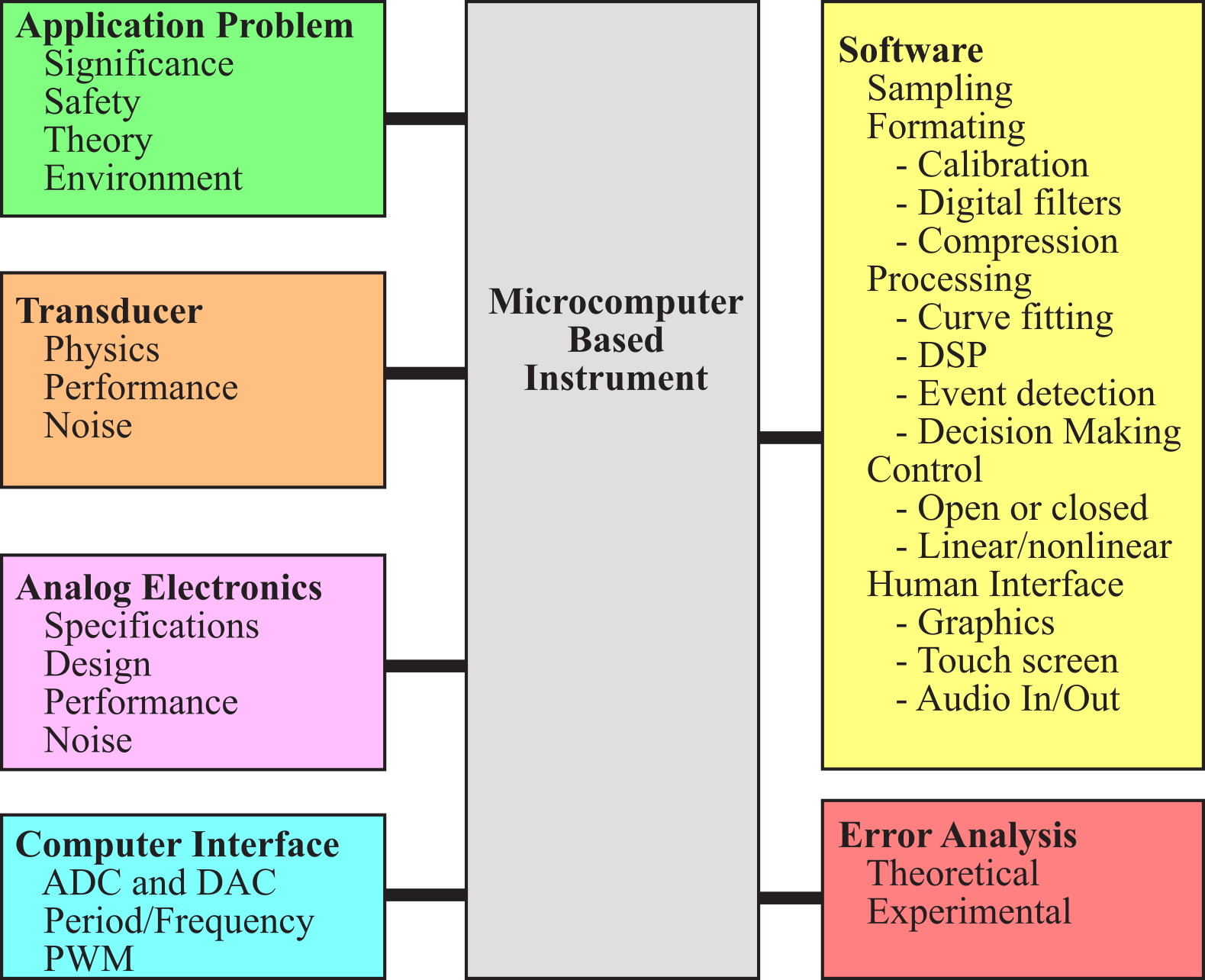
Figure 2.1.1. Individual components are integrated into a data acquisition system.
The measurand is the physical quantity, property, or condition that the system measures. In Figure 2.1.2, the inputs to the microcontroller constitute a data acquisition system. In this chapter, we focus on using the ADC to collect data. In Section 8.2, we will use the timer to collect frequency, period, pulse width or phase data. When we add outputs to affect the real world it becomes a control system. Control systems will be presented in Chapter 8. The measurand can be inherent to the object (like position, mass, or color), located on the surface of the object (like the human EKG, or surface temperature), located within the object (e.g., fluid pressure, or internal temperature), or separated from the object (like emitted radiation.)
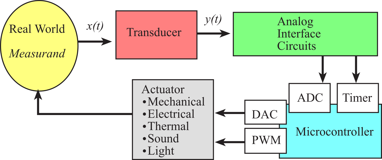
Figure 2.1.2. Signal paths a control system.
In general, a transducer converts one energy type into another. In Latin, transducere means "to lead across". In the context of this book, the transducer converts the measurand into an electrical signal that can be processed by the system. Typically, a transducer has a primary sensing element and a variable conversion element. The primary sensing element interfaces directly to the object and converts the measurand into a more convenient energy form. The output of the variable conversion element is an electrical signal that depends on the measurand. For example, the primary sensing element of a pressure transducer is the diaphragm, which converts pressure into a displacement of a plunger. The variable conversion element is a strain gauge that converts the plunger displacement into a change in electrical resistance. If the strain gauge is placed in a bridge circuit, the voltage output is directly proportional to the pressure. Some transducers perform a direct conversion without having a separate primary sensing element and variable conversion element.
The data acquisition system contains signal processing, which manipulates the transducer signal output to select, enhance, or translate the signal to perform the desired function, usually in the presence of disturbing factors. The signal processing can be divided into stages. The analog signal processing consists of instrumentation electronics, isolation amplifiers, amplifiers, analog filters, and analog calculations. The first analog processing involves calibration signals and preamplification. Calibration is necessary to produce accurate results. An example of a calibration signal is the reference junction of a thermocouple. The second stage of the analog signal processing includes filtering and range conversion. The analog signal range should match the ADC analog input range. Examples of analog calculations include RMS calculation, integration, differentiation, peak detection, threshold detection, phase lock loops, AM FM modulation/demodulation, and the arithmetic calculations of addition, subtraction, multiplication, division, and square root.
The data conversion element performs the conversion between the analog and digital domains. This part of the system includes hardware and software computer interfaces, ADC, DAC, S/H, analog multiplexer, and calibration references. The ADC converts the analog signal into a digital number. In Section 8.2, we will see that the period, pulse width, and frequency measurement approaches provide low-cost high-precision alternatives to the traditional ADC.
The digital signal processing includes data acquisition (sampling the signal at a fixed rate), data formatting (scaling, calibration), data processing (filtering, curve fitting, FFT, event detection, decision making, analysis), and control algorithms (open or closed loop).
The human interface includes the input and output which is available to the human operator, see Chapter 3. The advantage of computer-based system is the sophistication of the human interface. The inputs to the system can be audio (voice), visual (light pens, cameras), or tactile (keyboards, touch screens, buttons, switches, joysticks, roller balls). The outputs from the system can be numeric displays, CRT screens, graphs, buzzers, bells, lights, and voice.
Whenever reporting specifications of our system, it is important to give the definitions of each parameter, the magnitudes of each parameter, and the experimental conditions under which the parameter was measured. This is because engineers and scientists apply a wide range of interpretations for these terms.
2.1.1. Accuracy
The system accuracy is the absolute error referenced to the National Institute of Standards and Technology (NIST) of the entire system including transducer, electronics, and software. Let xmi be the values measured by the system and let xti be the true values from NIST references. In some applications, the signal of interest is a relative quantity (like temperature or distance between objects). For relative signals, accuracy can be appropriately defined in many ways:

In other applications, the signal of interest is an absolute quantity. For these situations, we can specify errors as a percentage of reading or as a percentage of full scale:

Observation: The definitions of accuracy, resolution, and precision vary considerably in technical literature. It is good practice to include both the definitions of your terms as well as their values in your technical communication.
: When would it be dishonest to use accuracy of full scale? I.e., when would accuracy of reading be more honest?
Since the Celsius and Fahrenheit temperature scales have arbitrary zeroes (e.g., 0 °C is the freezing point of water), it is inappropriate to specify temperature error as a percentage of reading or as a percentage of full scale when Celsius and Fahrenheit scales are used. When specifying temperature error, we should use average accuracy, maximum error, or standard error. These errors have units of °C or °F.
Typically, we calibrate a quantitative data acquisition system by determining a transfer function that relates the measured variable, x, to raw measurements such as the ADC sample. Accuracy is limited by two factors: resolution and calibration drift. Calibration drift is the change in the transfer function occurring over time used to calculate the measured variable from the raw measurements.
If we observe event B following event A, a common fallacy is to believe A caused B. This errant logic is called post hoc ergo propter hoc. "I washed my car, then it started raining. Clearly, I caused it to rain."
2.1.2. Resolution
The system resolution is the smallest input signal difference, Δx that can be detected by the entire system including transducer, electronics, and software. The resolution of the system is sometimes limited by noise processes in the transducer itself (e.g., thermal imaging) and sometimes limited by noise processes in the electronics (e.g., thermistors, RTDs, and thermocouples). The coefficient of variation is the standard deviation divided by the mean, CV is σ/μ. 1/CV is μ/σ is a simple estimate of the signal to noise ratio (SNR).
: Imagine you are a baseball pitcher. The catcher positions her mitt at the place she wishes you to throw the ball. You throw many baseballs at the catcher. Using this analogy describe the difference between accuracy and resolution.
The spatial resolution (or spatial frequency response) of the transducer is the smallest distance between two independent measurements. The size and mechanical properties of the transducer determine its spatial resolution. When measuring temperature, a metal probe will disturb the existing medium temperature field more than a glass probe. Hence, a glass probe has a smaller spatial resolution than a metal probe of the same size. Noninvasive imaging systems exhibit excellent spatial resolution because the system does not disturb the medium being measured. The spatial resolution of an imaging system is the medium surface area from which the radiation originates, which is eventually focused onto the detector during the imaging of a single pixel. Another name of spatial resolution is the instantaneous field of view, IFOV. When measuring force, pressure, or flow, spatial resolution is the effective area over which the measurement is obtained. Another way to illustrate spatial resolution is to attempt to collect a 2-D or 3-D image of the measurand. The spatial resolution is the distance between points.
2.1.3. Precision
Precision is the number of distinguishable alternatives, nx, from which the given result is selected. Precision can be expressed in alternatives, bits or decimal digits. Consider a thermometer system with a temperature range of 0 to 100 °C. The system displays the output using 3 digits (e.g., 12.3 °C). In addition, the system can resolve each temperature T from the temperature T+0.1°C. This system has 1001 distinguishable outputs, and hence has a precision of 1001 alternatives, about 10 bits, or 3 decimal digits. For a linear system, there is a simple relationship between range (rx), resolution (Δx) and precision (nx). Range is equal to resolution times precision
rx (100˚C) = Δx (0.1°C) * nx (1001 alternatives)
where "range" is the maximum minus minimum temperature, and precision is specified in terms of number of alternatives. Three decimal digits (precision=1000 alternatives) is approximately equal to ten binary digits (precision=1024 alternatives.)
: Let n be an integer. Consider 103*n (i.e., thousand, million, billion etc.) What value of m, makes 2m approximately equal to 103*n?
: Consider a system with a precision of 20 bits. What is the equivalent precision in decimal digits?
2.1.4. Reproducibility and Repeatability
Reproducibility (or repeatability) is a parameter that specifies whether the system has equal outputs given identical inputs over time. This parameter can be expressed as the full range or standard deviation of output results given a fixed input, where the number of samples and time interval between samples are specified. One of the largest sources of this type of error comes from transducer drift. Statistical control is a similar parameter based on a probabilistic model that also defines errors due to noise. The parameter includes the noise model (e.g., normal, chi-squared, uniform, salt and pepper) and the parameters of the model (e.g., average, standard deviation).

2.1.5. Quantitative versus qualitative data acquisition
We can classify system as a Quantitative DAS, if the specifications can be defined explicitly in terms of desired range (rx), resolution (∆x), precision (nx), and frequencies of interest (fmin to fmax). If the specifications are more loosely defined, we classify it as a Qualitative DAS. Examples of qualitative systems include those which mimic the human senses where the specifications are defined using terms like "sounds good", "looks pretty", and "feels right." Other qualitative systems involve the detection of events. We will consider two examples, a burglar detector, and a system to diagnose cancer. For binary detection systems like the presence/absence of a burglar or the presence/absence of cancer, we define a true positive (TP) when the condition exists (there is a burglar) and the system properly detects it (the alarm rings.) We define a false positive (FP) when the condition does not exist (there is no burglar) but the system thinks there is (the alarm rings.) A false negative (FN) occurs when the condition exists (there is a burglar) but the system does not think there is (the alarm is silent.) A true negative (TN) occurs when the condition does not exist (the patient does not have cancer) and the system properly detects it (the system says the patient is normal.) Prevalence is the probability the condition exists, sometimes called pre-test probability. In the case of diagnosing the disease, prevalence tells us what percentage of the population has the disease. Sensitivity is the fraction of properly detected events (a burglar comes and the alarm rings) over the total number of events (number of robberies.) It is a measure of how well our system can detect an event. For the burglar detector, a sensitivity of 1 means when a burglar breaks in the alarm will go off. For the diagnostic system, a sensitivity of 1 means every sick patient will get treatment. Specificity is the fraction of properly handled non-events (a patient doesn't have cancer and the system claims the patient is normal) over the total number of non-events (the number of normal patients.) A specificity of 1 means no people will be treated for a cancer they don't have. The positive predictive value of a system (PPV) is the probability that the condition exists when restricted to those cases where the system says it exists. It is a measure of how much we believe the system is correct when it says it has detected an event. A PPV of 1 means when the alarm rings, the police will come and arrest a burglar. Similarly, a PPV of 1 means if our system says a patient has the disease, then that patient is sick. The negative predictive value of a system (NPV) is the probability that the condition does not exist when restricted to those cases where the system says it doesn't exist. A NPV of 1 means if our system says a patient doesn't have cancer, then that patient is not sick. Sometimes the true negative condition doesn't really exist (how many times a day does a burglar not show up at your house?) If there are no true negatives, only sensitivity and PPV are relevant.
Prevalence = (TP + FN) / (TP + TN + FP + FN)
Sensitivity = TP / (TP + FN)
Specificity = TN / (TN + FP)
PPV = TP / (TP + FP)
NPV = TN / (TN + FN)
2.2. Transducers
In this section, we will start with quantitative performance measures for the transducer. Next, specific transducers will be introduced. Rather than give an exhaustive list of all available transducers, the intent in this section is to illustrate the range of possibilities, and to provide specific devices to use in the design sections later in the chapter.
2.2.1. Static Transducer Specifications
The input or measurand is x. The output is y. A transducer converts x into y, see Figure 2.2.1.

Figure 2.2.1. Transducers in this book convert a physical signal into an electrical signal.
The static sensitivity is the slope, m, of the straight line through the static calibration curve that gives minimal mean squared error. Let xi, yi be the input/output signals of the transducer. The linearity is a measure of the straightness of the static calibration curve. Let yi = f(xi) be the transfer function of the transducer. A linear transducer satisfies:
f(ax1+bx2) = af(x1)+bf(x2)
for any arbitrary choice of the constants a and b. Let yi = mxi+b be the best fit line through the transducer data. Linearity (or deviation from it) as a figure-of-merit can be expressed as percentage of reading or percentage of full scale. Let ymax be the largest transducer output.

Two definitions for sensitivity are used for temperature transducers. The static sensitivity is:
m = dy/dx
If the transducer is linear then the static sensitivity is the slope, m, of the straight line through the static calibration curve which gives the minimum mean squared error. If xi and yi represent measured input/output responses of the transducer, then the least squares fit to yi=mxi +b is

Unfortunately, transducers are often sensitive to factors other than the signal of interest. Environmental issues involve how the transducer interacts with its external surroundings (e.g., temperature, humidity, pressure, motion, acceleration, vibration, shock, radiation fields, electric fields and magnetic fields.) Specificity is a measure of relative sensitivity of the transducer to the desired signal compared to the sensitivity of the transducers to these other unwanted influences. A transducer with a good specificity will respond only to the signal of interest and be independent of these disturbing factors. On the other hand, a transducer with a poor specificity will respond to the signal of interest as well as to some of these disturbing factors. If all these disturbing factors are grouped together as noise, then the signal-to-noise ratio (S/N) is a quantitative measure of the specificity of the transducer.
The input range is the allowed range of input, x. The input impedance is the phasor equivalent of the steady state sinusoidal effort (voltage, force, pressure, temperature) input variable divided by the phasor equivalent of steady state flow (current, velocity, flow, heat flow) input variable. The output signal strength of the transducer can be specified by the output resistance, Rout, and output capacitance, Cout, see Figure 2.2.2.

Figure 2.2.2. Output model of a transducer.
: In general, it is better for the transducer to have a large or small input impedance?
: In general, it is better for the transducer to have a large or small output impedance?
The zero drift is the change in the static sensitivity curve intercept, b, as a function of time or another factor (see Figure 2.2.3). The sensitivity drift is the change in the static sensitivity curve slope, m, as a function of time or some other factor. These drift factors determine how often the transducer must be calibrated. For example, thermistors have a drift much larger than that of RTDs or thermocouples. Transducers may be aged at high temperatures for long periods of time to improve their reproducibility.

Figure 2.2.3. The two types of transducer drift: sensitivity drift and zero drift.
: Consider a transducer with a large drift. Which system parameter will be most affected: accuracy or resolution?
The transducer is often a critical device involving both the cost and performance of the entire system. A quality transducer may produce better signals but at an increased cost. An important manufacturing issue is the availability of components. The availability of a device may be enhanced by having a second source (more than one manufacturer produces the device). The use of standard cables and connectors will simplify the construction of your system. The power requirements, size and weight of the device are important in some systems, and thus should be considered when selecting a transducer.
2.2.2. Dynamic Transducer Specifications
The transient response is the combination of the delay phase, the slewing phase, and the ringing phase as shown in Figure 2.2.4. The total transient response is the time for the output, y(t), to reach 99% of its final value after a step change in input, x(t)=u0(t).

Figure 2.2.4. The step response often has delay, slewing and ringing phases.
The transient response of a temperature transducer to a sudden change in signal input can sometimes be approximated by an exponential equation (assuming first-order response):
y(t) = yf + (y0- yf) e-t/τ
where y0 and yf are the initial and final transducer outputs respectively. The time constant, τ, of a transducer is the time to reach 63.2% of the final output after the input is instantaneously increased. This time is dependent on both the transducer and the experimental setup. Manufacturers often specify the time constant of thermistors and thermocouples in well-stirred oil (fastest) or still air (slowest). In your applications, one must consider the situation. If the transducer is placed in a high flow liquid like an artery or a water pipe, it may be reasonable to use the stirred oil time constant. If the transducer is in air or embedded in a solid, then thermal conduction in the medium will determine the time constant almost independently of the transducer.
The frequency response is a standard technique to describe the dynamic behavior of linear systems. Let y(t) be the system response to x(t). Let
x(t) = Asin(ωt) y(t) = Bsin(ωt+φ) ω= 2 π f
The magnitude B/A and the phase ϕ responses are both dependent on frequency. Differential equations can be used to model linear transducers. Let x(t) be the time domain input signal. Let X(jω) be the frequency domain input signal. Let y(t) be the time domain output signal. Let Y(jω) be the frequency domain output signal, see Table 2.2.1.
|
Classification |
differential equation |
gain response |
phase response |
|
ZERO ORDER |
y(t) = m x(t) |
Y/X = m = static sensitivity |
|
|
FIRST ORDER |
y'(t) + a y(t) = b x(t) |
Y/X =b/sqrt(a2+ω2) |
φ= arctan(-ω/a) |
|
SECOND ORDER |
y''(t) + a y'(t) + b y(t) = c x(t) |
|
|
|
TIME DELAY |
y(t) = x(t-T) |
Y/X = exp(-jωT) |
|
Table 2.2.1. Classifications of simple linear systems.
: What type of system has a response as plotted in Figure 2.2.4?
2.2.3. Nonlinear Transducers
Nonlinear characteristics include hysteresis, saturation, bang-bang, breakdown, and dead zone. Hysteresis is created when the transducer has memory. We can see in Figure 2.2.5 that when the input was previously high it falls along the higher curve, and when the input was previously low it follows along the lower curve. Hysteresis will cause a measurement error, because for any given sensor output, y, there may be two possible measurand inputs. Saturation occurs when the input signal exceeds the useful range of the transducer. With saturation, the sensor does not respond to changes in input value when the input is either too high or too low. Breakdown describes a second possible result that may occur when in the input exceeds the useful range of the transducer. With breakdown, the sensor output changes rapidly, usually the result of permanent damage to the transducer. Hysteresis, bang bang and dead zone all occur within the useful range of the transducer. Bang bang is a sudden large change in the output for a small change in the input. If the bang bang occurs predictably, then it can be corrected for in software. A dead zone is a condition where a large change in the input causes little or no change in the output. Dead zones cannot be corrected for in software, thus if present will cause measurement errors.

Figure 2.2.5. Nonlinear transducer responses.
There are many ways to model nonlinear transducers. A nonlinear transducer can be described as a piecewise linear system. The first step is to divide the range of x into a finite subregions, assuming the system is linear in each subregion. The second step is to solve the coupled linear systems so that the solution is continuous. Another method to model a nonlinear system is to use empirically determined nonlinear equations. The first step in this approach is to observe the transducer response experimentally. Given a table of x and y values, the second step is to fit the response to a nonlinear equation. Engineers call these empirical fits performance maps.
A third approach to modeling a nonlinear transducer uses a lookup table located in memory. This method is convenient and flexible. Let x be the measurand and y be the transducer output. The table contains x values and the measured y value is used to index into the table. Sometimes a small table coupled with linear interpolation achieves equivalent results to a large table.
Monotonic behavior means the input/output function of the transducer is always increasing or always decreasing. A monotonic function has a mathematical inverse. A monotonic transducer allows us to measure the output of the transducer and then use the inverse function to determine the input.
A nonmonotonic response is an input/output function that does not have a mathematical inverse. For example, if two or more input values yield the same output value, then the transducer is nonmonotonic. Software will have a difficult time correcting a nonmonotonic transducer. For example, the Sharp GP2Y0A21YK IR distance sensor has a transfer function as shown in Figure 2.2.6.
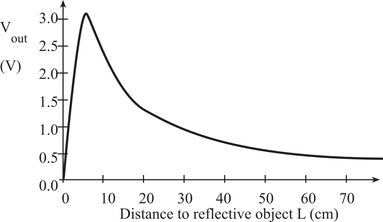
Figure 2.2.6. The Sharp IR distance sensors are nonmonotonic. The GP2Y0A41SK0F range is 80 cm.
If you read a Sharp IR sensor voltage of 2 V, you cannot tell if the object is 3 cm away or 12 cm away. The RSLK robot has three of these sensors, positioned more than 3 cm from the edge of the robot, eliminating the nonmonotonic portion of the sensor, see Figure 2.2.7.
Figure 2.2.7. The RSLK can have either the GP2Y0A41SK0F (range 30 cm) or the GP2Y0A21YK0F (range 80 cm) distance sensor.
: What transducer properties allow software to convert its nonlinear response into an accurate measurement system?
2.2.4. Position Transducers
One of the simplest methods to convert position into an electrical signal uses a position sensitive potentiometer. These devices are inexpensive to build and are sensitive to small displacements. The transducer is constructed from a potentiometer. The fixed part of the potentiometer is called the frame, and the movable part is the armature. The armature is free to move up and down along the measurement axis, see Figure 2.2.8. The frame is fixed and the armature is attached to the object being measured. The total electrical resistance of the transducer is fixed, but the resistance to the slide arm varies with distance, d.
Rout = Rmax*d/dmax
where dmax is distance at full scale and Rmax is the resistance at full scale. If the material in the potentiometer has uniform resistance, then Rout will be linearly related to displacement, d. The disadvantages of this transducer are its low frequency response, its high mechanical input impedance, and it degenerates with time. Nevertheless, this type of transducer exposes the basic principles of signal conversion. We can interface it with an ADC or input capture, see Section 8.2.
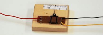
Figure 2.2.8. Potentiometer-based position sensor.
: What could cause the transducer in Figure 2.2.8 to have drift?
The transducer in Figure 2.2.6 uses IR light to measure distance to a reflecting object. These sensors require energy when it emits an IR pulse, so placing a 10 μF near the +5V power line of the sensor reduces noise on other components. If the object is more than 6 cm away, the output voltage is inversely related to voltage. If N is the ADC sample, then distance can be calculated as
d = c/N where c is a calibration constant
Another method to measure the distance between two objects is to transmit an ultrasonic wave from one object at the other and listen for the reflection (Figure 2.2.9). The system must be able to generate the sound pulse, hear the echo and measure the time, tin, between pulse and echo. If the speed of sound, c, is known, then the distance, d, can be calculated. Our microcontrollers also have mechanisms to measure the pulse width tin. See Section 8.2.
d = c tin / 2
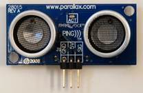

Figure 2.2.9. An ultrasonic pulse-echo transducer measures the distance to an object, Ping))).
: Is the ultrasonic transducer linear or nonlinear?
: What could cause an ultrasonic transducer to drift?
2.2.5. Sound Transducers
A microphone is a type of displacement transducer. Sound waves, which are pressure waves travelling in air, cause a diaphragm to vibrate, and the diaphragm motion causes the distance between capacitor plates to change. This variable capacitance creates a voltage, which can be amplified and recorded. The electret condenser microphone (ECM) is an inexpensive choice for converting sound to analog voltage. Electret microphones are used in consumer and communication audio devices because of their low cost and small size. For applications requiring high sensitivity, low noise, and linear response, we could use the dynamic microphone, like the ones used in high-fidelity audio recording equipment. The ECM capsule acts as an acoustic resonator for the capacitive electret sensor shown in Figure 2.2.10. The ECM has a Junction Field Effect Transistor (JFET) inside the transducer providing some amplification. This JFET requires power as supplied by the R1 resistor. This local amplification allows the ECM to function with a smaller capsule than typically found with other microphones. ECM devices are cylindrically shaped, have a diameter ranging from 3 to 10 mm, and have a thickness ranging from 1 to 5 mm.
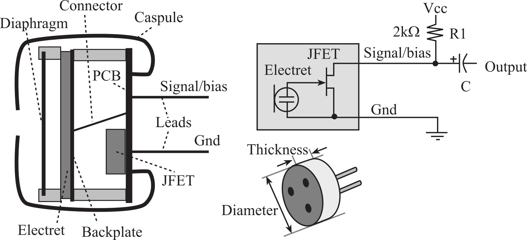
Figure 2.2.10. Physical and electrical view of an ECM with JFET buffer (Vcc depends on microphone)
An ECM consists of a pre-charged, non-conductive membrane between two plates that form a capacitor. The backplate is fixed, and the other plate moves with sound pressure. Movement of the plate results in a capacitance change, which in turn results in a change in voltage due to the non-conductive, pre-charged membrane. An electrical representation of such an acoustic sensor consists of a signal voltage source in series with a source capacitor. The most common method of interfacing this sensor is a high-impedance buffer/amplifier. A single JFET with its gate connected to the sensor plate and biased as shown in Figure 2.2.10 provides buffering and amplification. The capacitor C provides high-pass filtering, so the voltage at the output will be less than ±100 mV for normal voice. Audio microphones need additional amplification and band-pass filtering. Typical audio signals exist from 100 Hz to 10 kHz. The presence of the R1 resistor is called "phantom biasing". The electret has two connections: Gnd and Signal/bias. Typically, the metallic capsule is connected to Gnd. Interfacing the microphone is presented in Section 5.4.1.
2.2.6. Force and Pressure Transducers
A common device to measure force and pressure is the strain gauge. See Figure 2.2.11. As a wire is stretched its length increases and its cross-sectional area decreases. These geometric changes cause an increase in the electrical resistance of the wire, R. The transducer is constructed with four sets of wires mounted between a stationary member (frame) and a moving member (armature.) As the armature moves relative to the frame, two wires are stretched (increase in R1 R4), and two wires are compressed (decrease in R2 R3), as shown in Figure 2.2.12. The strain gauge is a displacement transducer, such that a change in the relative position between the armature and frame, Δx, causes a change in resistance, ΔR. The sensitivity of a strain gauge is called its gauge factor.
G = (ΔR/R)/ Δx/x)
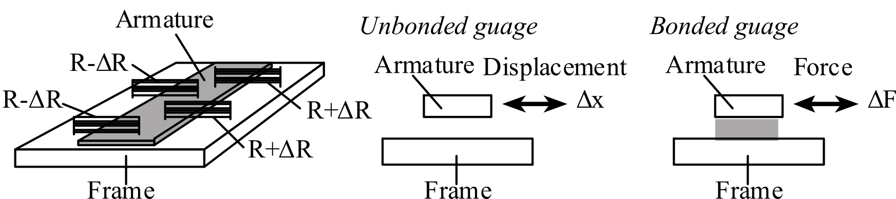
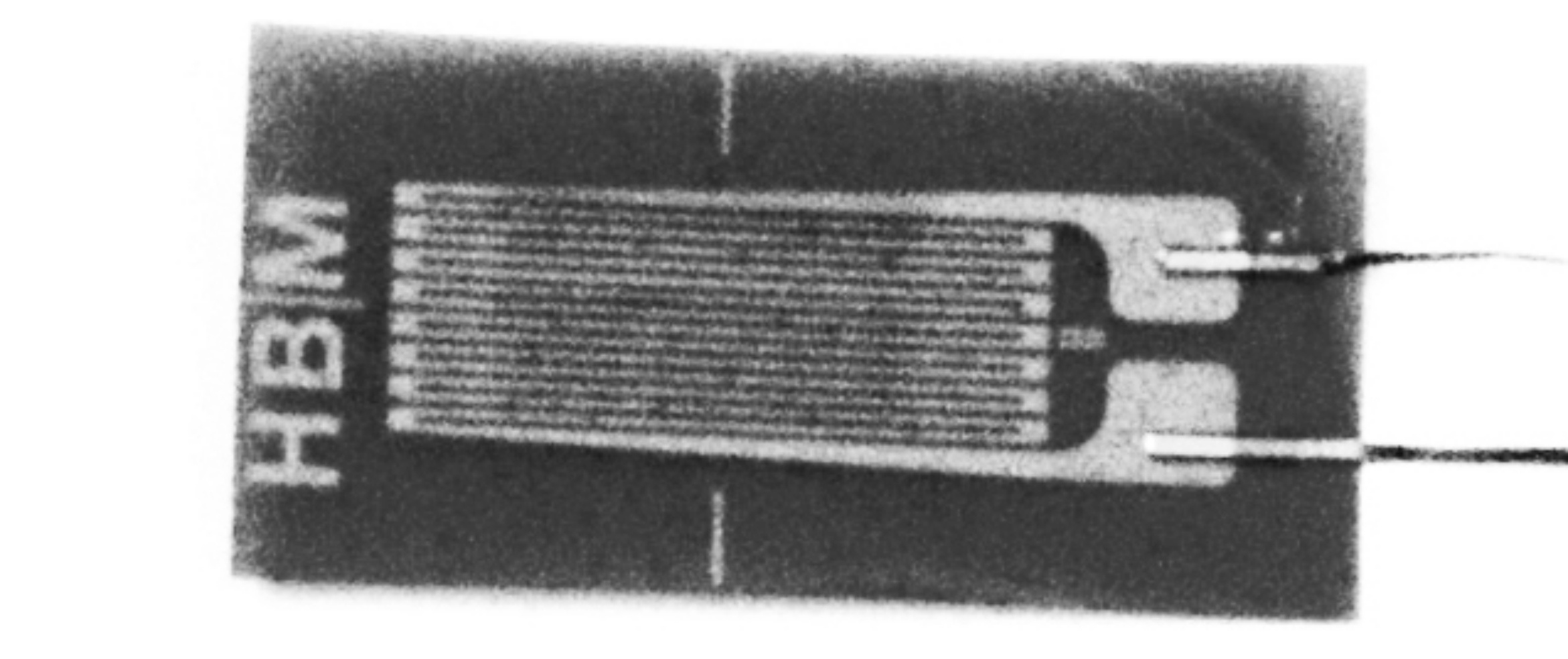
Figure 2.2.11. Strain gauges used for force or pressure measurement.
The gauge factor for an Advance strain gauge is 2.1. The typical resistance, R, is 120 Ω. If the gauge is bonded onto a material with a spring characteristic:
F = -k x
then the transducer can be used to measure force. The wires each have a significant temperature drift. When the four wires are placed into a bridge configuration, the temperature dependence cancels. A high gain, high input impedance, high CMRR differential amplifier is required, as shown in Figure 2.2.12.
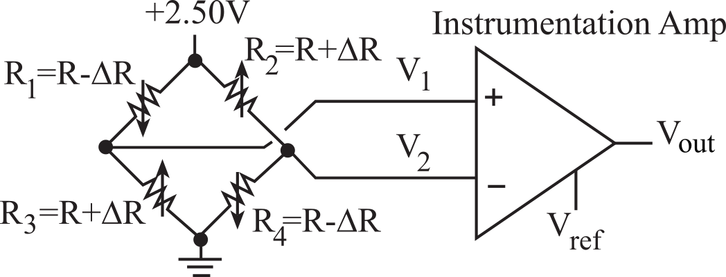
Figure 2.2.12. Four strain gauges are placed in a bridge configuration.
: Define the input impedance of a strain gauge?
Force and pressure sensors can also be made from semiconductor materials. These silicon sensors can be made much smaller than strain gauges but tend to be much more nonlinear. A force sensing resistor (FSR) is made with a resistive film and converts force into resistance. These sensors are low cost and easy to interface but tend to be quite nonlinear.
2.2.7. Temperature Transducers
Thermistors are a popular temperature transducer made from a ceramic-like semiconductor. A NTC (negative temperature coefficient) thermistor is made from combinations of metal oxides of manganese, nickel, cobalt, copper, iron, and titanium. A mixture of milled semiconductor oxide powders and a binder is shaped into the desired geometry. The mixture is dried and sintered (under pressure) at an elevated temperature. The wire leads are attached, and the combination is coated with glass or epoxy. By varying the mixture of oxides, a range of resistance values from 30 Ω to 20 MΩ (at 25 °C) is possible.
A precision thermometer, an ohmmeter, and a water bath are required to calibrate thermistor probes. The following empirical equation yields an accurate fit over a narrow range of temperature:
T = (1/(H0+H1*ln(R)) -273.15 where H0 and H1 are calibration coefficients
where T is the temperature in Celsius, and R is the thermistor resistance in ohms. It is preferable to use the ohmmeter function of the eventual instrument for calibration purposes so that influences of the resistance measurement hardware and software are incorporated into the calibration process.
The first step in the calibration process is to collect temperature (measured by a precision thermometer) and resistance data (measured by the ohmmeter process of the system). The thermistor(s) to be calibrated should be placed as close to the sensing element of the precision thermometer as possible. The water bath creates a stable yet controllable environment in which to perform the calibration.
A thermocouple is constructed by spot welding two different metal wires together. Probe transducers include a protective casing which surrounds the thermocouple junction. Probes come in many shapes including round tips, conical needles and hypodermic needles. Bare thermocouple junctions provide faster response but are more susceptible to damage and noise pickup. Ungrounded probes allow electrical isolation but are not as responsive as grounded probes. A spot weld is produced by passing a large current through the metal junction that fuses the two metals together. If the wires form a loop, and the junctions are at different temperatures, then a current will flow in the loop. This thermal to electrical energy conversion is called the Seebeck effect (see Figure 2.2.13). If the temperature difference is small, then the current, I, is linearly proportional to the temperature difference T1-T2.
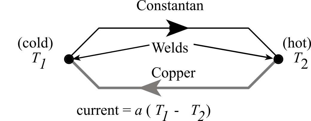
Figure 2.2.13. When the two thermocouple junctions are at different temperatures current will flow.
If the loop is broken, and an electrical voltage is applied, then heat will be absorbed at one junction and released at the other. This electrical to thermal energy conversion is called the Peltier effect, see Figure 2.2.14. If the voltage is small, then the heat transferred is linearly proportional to the voltage, V.

Figure 2.2.14. When voltage is applied to two thermocouple junctions heat will flow.
If the loop is broken, and the junctions are at different temperatures, then a voltage will develop because of the Seebeck effect, see Table 2.2.2. If the temperature difference is small, then the voltage, V, is nearly linearly proportional to the temperature difference T1-T2. An amplifier is required to match the transducer output range to the ADC range, see Figure 2.2.15. Under most conditions we will add an analog low pass filter.
|
Type - Thermocouple |
μV/˚C at 20˚C |
Useful range °C |
Comments |
|
T - Copper/Constantan |
45 |
-150 to +350 |
Moist environment |
|
J - Iron/Constantan |
53 |
-150 to +1000 |
Reducing environment |
|
K - Chromel/alumel |
40 |
-200 to +1200 |
Oxidizing environment |
|
E - Chromel/constantan |
80 |
0 to +500 |
Most sensitive |
|
R S - Platinum/platinum-rhodium |
6.5 |
0 to +1500 |
Corrosive environment |
|
C - Tungsten/rhenium |
12 |
0 to 2000 |
High temperature |
Table 2.2.2. Temperature sensitivity and range of various thermocouples.
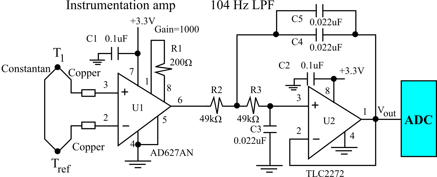
Figure 2.2.15. A thermocouple converts temperature difference to voltage.
Thermocouples are characterized by: 1) low impedance (resistance of the wires), 2) low temperature sensitivity (45 μV/˚C for copper/constantan), 3) low-power dissipation, 4) fast response (because of the metal), 5) high stability (because of the purity of the metals), and 6) interchangeability (again because of the physics and the purity of the metals).
If the temperature range is less than 25°C, then the linear approximation can be used to measure temperature. Let N be the digital sample from the ADC for the unknown medium temperature, T1. A calibration is performed under the conditions of a constant reference temperature: typically, one uses the extremes of the temperature range (Tmin and Tmax). A precision thermometer system is used to measure the "truth" temperatures. Let Nmin and Nmax be the digital samples at Tmin and Tmax respectively. Then the following equation can be used to calculate the unknown medium temperature from the measured digital sample.

Because the thermocouple response is not exactly linear, the errors in the above linear equation will increase as the temperature range increases. For systems with a larger temperature range, a quadratic equation can be used,
T1 = H0 + H1*N + H2*N2
where H0 H1 and H2 are determined by calibration of the system over the range of interest.
: Define the input impedance of a temperature sensor like a thermistor or thermocouple?
Table 2.2.3 lists the tradeoffs between thermistors and thermocouples.
|
Thermistors |
Thermocouples |
|
More sensitive |
More sturdy |
|
Better temperature resolution |
Faster response |
|
Less susceptible to noise |
Inert, interchangeable V vs. T curves |
|
Less thermal perturbation |
Requires less frequent calibration |
|
Does not require a reference |
More linear |
Table 2.2.3. Tradeoffs between thermistors and thermocouples.
2.3. Analog to Digital Converters
2.3.1. ADC Parameters
An ADC converts an analog signal into digital form. The input signal is usually an analog voltage (Vin), and the output is a binary number. The ADC precision is the number of distinguishable ADC inputs (e.g., 4096 alternatives, 12 bits). The ADC range is the maximum and minimum ADC input (volts, amps). The ADC resolution is the smallest distinguishable change in input (volts, amps). The resolution is the change in input that causes the digital output to change by 1. Figure 2.3.1 shows a distance sensor interfaced to an ADC on the RSLK robot.
Range(volts) = Precision(alternatives) * Resolution(volts)
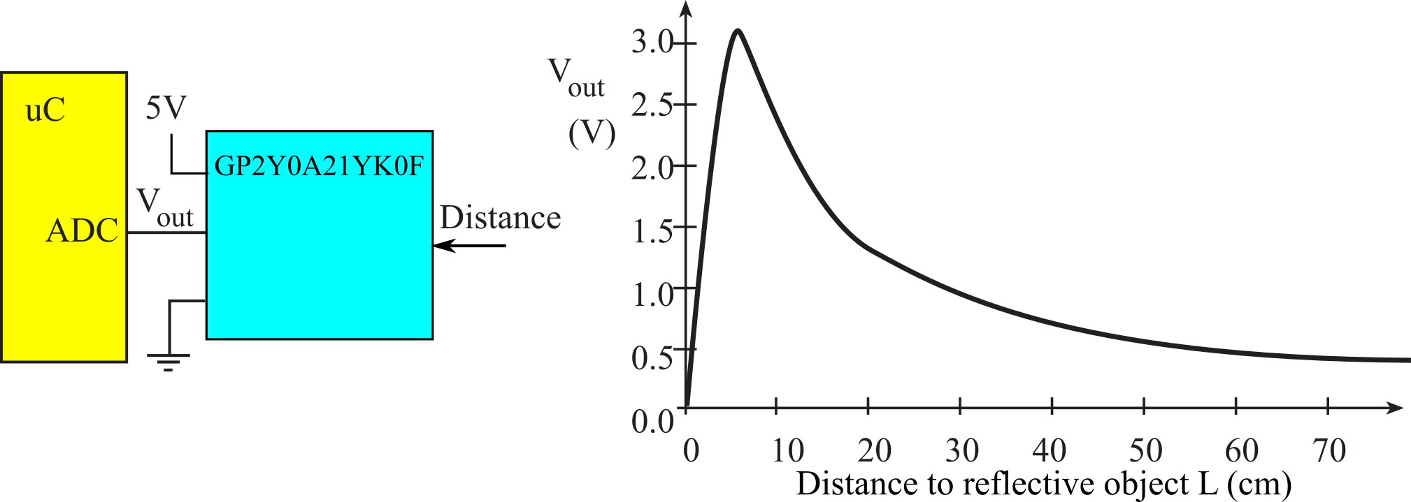
Figure 2.3.1. The GP2Y0A41SK0F distance sensor is connected to the ADC converter.
This tool allows you to
see the operation of a distance sensors on the RSLK robot. Distance
is the parameter to be measured, and it is defined as the distance in cm from
the robot to the wall at the left of the robot. The GP2Y0A41SK0Fsensor has
three terminals, as shown in Figure 2.3.1, such voltage Vout at the ADC converter
nonlinearly depends on distance.
The Digital value of the ADC conversition linearly depends on the
analog input, Vout.
The software will convert the Digital value into the Fixed_point part
of a decimal fixed-point number, with a resolution of 0.01cm. 293152 and -214 are calibration constants.
Fixed_point = 2931520/(Digital-214);
Exercise 1: Drag the robot to about 10cm, see Vout is about 2.5V and Fixed_point is about 1000.
Exercise 2: Drag the robot between 8 and 80 cm and compare the true distance with Fixed_point.
Exercise 3: Drag the robot between 1 and 8 cm and notice the large measurement errors.
Normally we don't specify accuracy for just the ADC, but rather we give the accuracy of the entire system (including transducer, analog circuit, ADC and software). Accuracy was described earlier in Section 2.1.1 as part of the systems approach to data acquisition systems. An ADC is monotonic if it has no missing codes. This means if the analog signal is a slow rising voltage, then the digital output will hit all values sequentially. The ADC is linear if the resolution is constant through the range. Let f(x) be the input/output ADC transfer function. One quantitative measure of linearity is the correlation coefficient of a linear regression fit of the f(x) responses. The ADC speed is the time to convert, called tc. The ADC cost is a function of the number and price of internal components.
The total harmonic distortion (THD) of a signal is a measure of the harmonic distortion present and is defined as the ratio of the sum of the powers of all harmonic components to the power of the fundamental frequency. Basically, it is a measure of all the noise processes in an ADC and usually is given in dB full scale. A similar parameter is signal-to-noise and distortion ratio (SINAD), which is measured by placing a pure sine wave at the input of the ADC (signal) and measuring the ADC output (signal plus noise). We can compare precision in bits to signal-to-noise ratio in dB using the relation dB = 20 log10(2n). For example, the 12-bit MAX1247 ADC has a SINAD of 73 dB. Notice that 20 log10(212) is 72 dB.
Dynamic range, expressed in dB, is defined as the range between the noise floor of a device and its specified maximum output level. The dynamic range is the range of signal amplitudes which the ADC can resolve. If an ADC can resolve signals from 1 mV to 1 V, it has a dynamic range of 20*log(1V/1mV) = 60dB. Dynamic range is important in communication applications, where signal strengths vary dramatically. If the signal is too large, it saturates the ADC input. If the signal is too small, it gets lost in the quantization noise.
The effective number of bits (ENOB) specifies the dynamic performance of an ADC at a specific input frequency and sampling rate. In an ideal situation, ADC error consists only of quantization noise (resolution = range/precision). As the input frequency increases, the overall noise (particularly in the distortion components) also increases, thereby reducing the ENOB and SINAD.
2.3.2. ADC Conversion Techniques
The most accurate method for ADC conversion is the successive approximation technique, as illustrated in Figure 2.3.1. A 12-bit successive approximation ADC is clocked 12 times. At each clock another bit is determined, starting with the most significant bit. For each clock, the successive approximation hardware issues a new "guess" on Vdac by setting the bit under test to a "1". If Vdac is now higher than the unknown input, Vin, then the bit under test is cleared. If Vdac is less than Vin, then the bit under test is remains 1. In this description, bit is an unsigned integer that specifies the bit under test. For a 12-bit ADC, bit goes 2048, 1024, 512, 256, 128, 64,...,1. Dout is the ADC digital output, and Z is the binary input that is true if Vdac is greater than Vin.
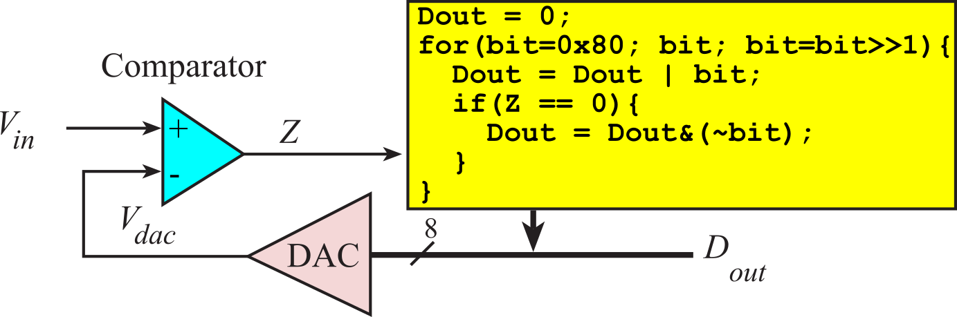
Figure 2.3.1. A 12-bit successive approximation ADC.
Observation: The speed of a successive approximation ADC relates linearly with its precision in bits.
Video 2.3.1. Successive Approximation
This tool allows you to
go through the motions of a ADC sample capture using successive
approximation. It is a game to demonstrate successive approximation.
There is a secret number between 0 to 63 (6-bit ADC) that the computer
has selected. Your job is to learn the secret number by making exactly 6
guesses. You can guess by entering numbers into the "Enter guess" field
and clicking "Guess". The Tool will tell you if the number you guess is
higher or lower than the secret number. When you have the answer, enter
it into the "Final answer" field and click the "Submit answer" button.
: With successive approximation, what is the strategy when making the first guess? For example, if you had an 8-bit ADC, what would be your first guess?
The sigma delta analog to digital converter is the method with the best resolution. It is used in many audio applications. It is a cost-effective approach to 16-bit 44 kHz sampling (CD quality audio). Sigma delta converters have a DAC, a comparator and digital processing similar to the successive approximation technique. While successive approximation converters have DACs with the same precision as the ADC, sigma delta converters use DACs with a much smaller precision than the ADC. A 1-bit DAC is simply a digital signal itself. The digital signal processing will run at a clock frequency faster than the overall ADC system, called oversampling. It uses complex signal processing to drive the output voltage V0 to equal the unknown input Vin in a time-averaged sense. The "delta" part of the sigma delta converter is the subtractor, where V1=V0-Vin. Next comes the "sigma" part that implements an analog integration. If V0 to equal the unknown input Vin in a time-averaged sense, then V2 will be zero. The comparator tests the V2 signal. If V2 is positive then V0 is made smaller. If V2 is negative then V0 is made larger. This DAC-subtractor-integrator-comparator-digital loop is executed at a rate much faster than the eventual digital output rate.
A very simple algorithm, shown in Figure 2.3.2 is run continuously. For every time through the outer while loop there is one ADC output. This algorithm is much too simple to be appropriate in an actual converter, but it does illustrate the sigma delta approach. For a 10-bit conversion, the DAC output rate is 1024 times the ADC conversion rate. We assume the input voltage, Vin, is between 0 and +3 V. DAC is an output of the sigma-delta processing that sets the 1-bit DAC. Z is the comparator output, which is an input to the signal processing.
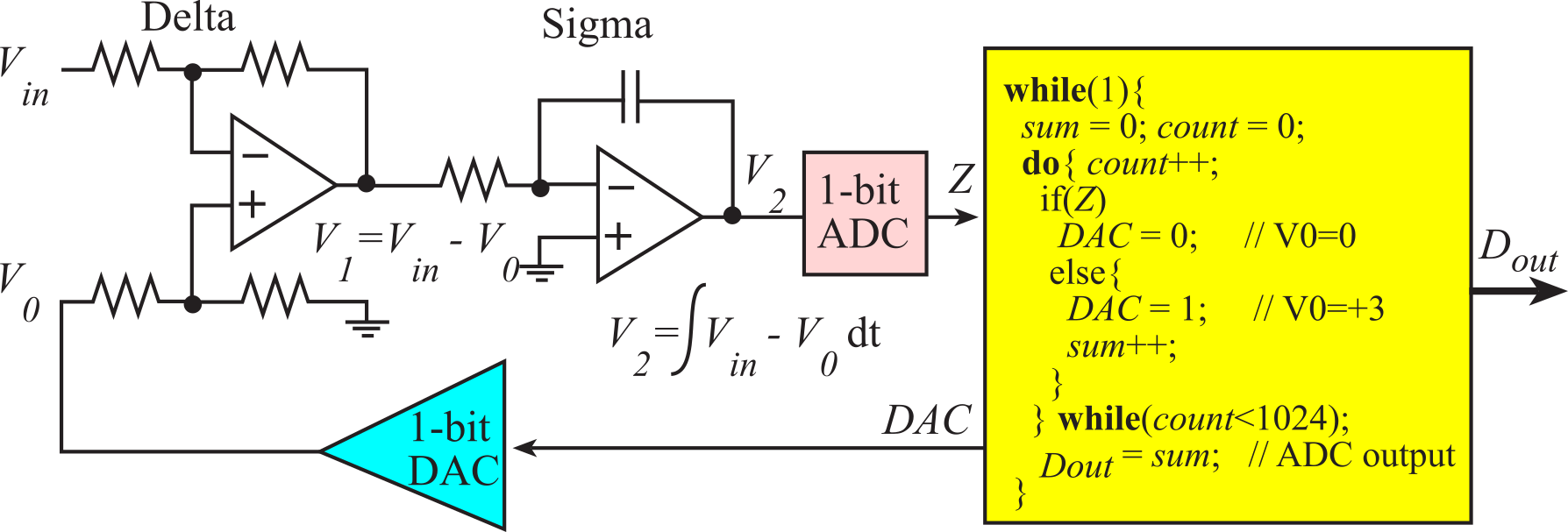
Figure 2.3.2. Block diagram of the sigma-delta ADC conversion technique.
In this very simple solution, the DAC is set to 1 (V0=+3) if Z is 0 (V2<0). Conversely, the DAC is set to 0 (V0=0) if Z is 1 (V2>0). Each time the DAC is set to 1, sum is incremented. At the end of 1024 passes, the value sum is recorded as the ADC sample. Since there are 1024 passes through the loop, sum will vary from 0 to 1023. For example, if the Vin is 1.5 V, then half of the DAC outputs will be 1 and the other half 0. This will make V0 oscillate between 0 and 3V, with a 50% duty cycle, V1 will oscillate between -1.5 and +1.5 with a 50 % duty cycle, and the time-averaged V2 will be zero.
A second example is illustrated in Figure 2.3.3. The input Vin is 2.25 V, so the output should be 2.25/3*1024 or 768. The sigma delta will adjust the DAC output so that V1=V0-Vin. is equal to 0 in a time-averaged sense. V1 is 2.25 V for 25% of the time and ‑0.75 V for 75% of the time. Three out of every four DAC outputs are high, so three out of every four time, V2 will be above 0. Therefore after 1024 times through the loop, 768 of them will increment sum, yielding the correct ADC result. If the Vin input rises, a higher percentage of DAC outputs will be high, increasing sum. If the Vin input falls, a lower percentage of DAC outputs will be high, decreasing sum.
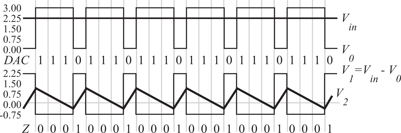
Figure 2.3.3. Example operation of a sigma-delta conversion.
In a real sigma-delta the overclock rate is typically 8 to 1 or 16 to 1. Multiple bits are obtained each time through the output-input cycle using DSP algorithms.
The fastest ADC technique is the flash. Flash converters are very expensive and very fast. It is fast because all the conversion sets run in parallel. Figure 2.3.4 shows a 3-bit flash. The linearity and monotonicity are determined by the eight resistors.The 8-to-3 bit encoder could be implemented with a 74HC148. The MAX104 is a ±5V, 1Gsps, 8-Bit ADC with on-chip 2.2GHz sample/hold. An 8-bit flash will have 256 comparators, and a 256-to-8 bit digital encoder.
Figure 2.3.4. Block diagram of a 3-bit flash ADC.
: Which ADC architecture has the best accuracy?
: Which ADC architecture is the fastest?
: Which ADC architecture has the best resolution?
: All ADC converters exhibit an exponential relationship. I.e., if the ADC is n bits, something in the ADC depends on 2n. What are the exponential relationships in the successive approximation, the sigma-delta, and the flash architectures?
2.3.3. Sample/Hold
A sample and hold (S/H) is an analog latch, illustrated in Figure 2.3.5. An alternative name for this analog component is track and hold. The purpose of the S/H is to hold the ADC analog input constant during the conversion. There is S/H at the input of most ADC, including the ones on the TM4C123 and MSPM0 microcontrollers. The first phase of most analog to digital conversions is the sampling phase, where the input voltage Vin, is recorded as a charge on the capacitor C.
Figure 2.3.5. The sample and hold has a digital input, an analog input and an analog output.
The digital input, Control, determines the S/H mode. The S/H is in sample mode, where Vout equals Vin, with the switch is closed. The S/H is in hold mode, Vout is fixed because the switch is open. The acquisition time is the time for the output to equal the input after the control is switched from hold to sample. This is the time to charge the capacitor C. The aperture time is the time for the output to stabilize after the control is switched from sample to hold. This is the time to open the switch, which is usually quite fast. The droop rate is the output voltage slope (dVout/dt) when Control equals hold. Normally the gain, K, should be one and the offset, Voff, should be zero. The gain and offset error specify how close is the Vout to the desired Vin when Control equals sample,
Vout = K Vin + Voff
To choose the capacitor, C:
1) One should use a high-quality capacitor with high
insulation resistance and low dielectric absorption.
2) A larger value of C will decrease (improve) the droop rate.
If the droop current is IDR, then the droop rate will be dVout/dt =IDR/C
3) A smaller C will decrease (improve) the acquisition time.
The system will require a sample and hold if the input signal could change during an ADC conversion. There will be a time during which the ADC samples the input voltage, tsamp. Let the maximum slew rate of the input signal be dVin/dt. If the slew rate times the sampling time is larger than the ADC resolution, we should add a sample and hold module to keep the analog input stable during conversion. The TM4C ADC modules have a built-in S/H.
2.4. Sampling Theory
2.4.1. Using Nyquist Theory to Determine Sampling Rate
There are two errors introduced by the sampling process. Voltage quantizing is caused by the finite word size of the ADC. The precision is determined by the number of bits in the ADC. If the ADC has n bits, then the number of distinguishable alternatives is
nz = 2n
Time quantizing is caused by the finite discrete sampling interval. The Nyquist Theorem states that if the signal is sampled at fs, then the digital samples only contain frequency components from 0 to 0.5 fs. Conversely, if the analog signal does contain frequency components larger than ½ fs, then there will be an aliasing error. Aliasing is when the digital signal appears to have a different frequency than the original analog signal. Simply put, if one samples a sine wave at a sampling rate of fs,
V(t) = A sin(2πft + φ)
is it possible to determine A f and φ from the digital samples? Nyquist Theory says that if fs is strictly greater than twice f, then one can determine A f and ϕ from the digital samples. In other words, the entire analog signal can be reconstructed from the digital samples. But if fs less than or equal to f, then one cannot determine A f and φ. In this case, the apparent frequency, as predicted by analyzing the digital samples, will be shifted to a frequency between 0 and ½ fs.
Discover the
Nyquist Theorem. In this animation, you control the analog signal
by dragging the handle on the left. Click and drag the handle up and
down to create the analog wave (the blue continuous wave). The signal is
sampled at a fixed rate (fs = 1Hz) (the red wave). The
digital samples are connected by straight red lines so you can see the
data as captured by the digital samples in the computer.
|
|
Exercise 1: If you move the handle up and down very slowly you will notice the digital representation captures the essence of the analog wave you have created by moving the handle. If you wiggle the handle at a rate slower than ½ fs, the Nyquist Theorem is satisfied and the digital samples faithfully capture the essence of the analog signal.
Exercise 2: However if you wiggle the handle quickly, you will observe the digital representation does not capture the analog wave. More specifically, if you wiggle the handle at a rate faster than ½ fs the Nyquist Theorem is violated causing the digital samples to be fundamentally different from the analog wave. Try wiggling the handle at a fast but constant rate, and you will notice the digital wave also wiggles but at an incorrect frequency. This incorrect frequency is called aliasing.
In Figure 2.4.1, the sampling rate is fixed at 1600 Hz and the signal frequency is varied. When sampling rate is exactly twice the input frequency, the original signal may or may not be properly reconstructed. In this specific case, it is frequency shifted (aliased) to DC and lost.
Figure 2.4.1. Aliasing does not occur when the sampling rate is more than twice the signal frequency.
When the sampling rate is slower than twice the input frequency, the original signal cannot be properly reconstructed. It is frequency-shifted (aliased) to a frequency between 0 and ½ fs. In this case the 1500 Hz wave was aliased to 100 Hz.
Video 2.4.1. Aliasing Demonstration: The Wagon Wheel Effect
Proving the Nyquist Theorem mathematically is beyond the scope of this course, but we can present a couple examples to support the basic idea of the Nyquist Theorem: we must sample at a rate faster than twice the rate at which signal itself is oscillating.
Video 2.4.2. The Nyquist Theorem Illustrated
Example 1) There is a long distance race with runners circling around an oval track and it is your job to count the number of times a particular runner circles the track. Assume the fastest time a runner can make a lap is 60 seconds. You want to read a book and occasionally look up to see where your runner is. How often to you have to look at your runner to guarantee you properly count the laps? If you look at a period faster than every 30 seconds you will see the runner at least twice per lap and properly count the laps. If you look at a period slower than every 30 seconds, you may only see the runner once per lap and not know if the runner is going very fast or very slow. In this case, the runner oscillates at most 1 lap per minute and thus you must observe the runner at a rate faster than twice per minute.
Example 2) You live on an island and want to take the boat back to the mainland as soon as possible. There is a boat that arrives at the island once a day, waits at the dock for 12 hours and then it sets sail to the mainland. Because of weather conditions, the exact time of arrival is unknown, but the boat will always wait at the dock for 12 hours before it leaves. How often do you need to walk down to the dock to see if the boat is there? If the boat is at the dock, you get on the boat and take the next trip back to the mainland. If you walk down to the dock every 13 hours, it is possible to miss the boat. However, if you walk down to the dock at a period less than every 12 hours, you'll never miss the boat. In this case, the boat frequency is once/day and you must sample it (go to the dock) greater than two times/day.
The choice of sampling rate, fs, is determined by the maximum useful frequency contained in the signal. One must sample at least twice this maximum useful frequency. Faster sampling rates may be required to implement a digital filter and other digital signal processing.
fs > 2 fmax
Even though the largest signal frequency of interest is fmax, there may be significant signal magnitudes at frequencies above fmax. These signals may arise from the input x, from added noise in the transducer or from added noise in the analog processing. Once the sampling rate is chosen at fs, then a low pass analog filter may be required to remove frequency components above ½ fs. A digital filter cannot be used to remove aliasing.
An interesting question arises: how do we determine the maximum frequency component in our input? If we know enough about our system, we might be able to derive an equation to determine the maximum frequency. For example, if a mechanical system consists of a mass, friction and a spring, then we can write a differential equation relating the applied force to the position of the object. The second way to find the maximum frequency component in our signal is to measure it with a spectrum analyzer.
Valvano Postulate: If fmax is the largest frequency component of the analog signal, then you must sample more than ten times fmax in order for the reconstructed digital samples to look like the original signal when plotted on a voltage versus time graph.
2.4.2. How Many Bits Does One Need for the ADC?
The choice of the ADC precision is a compromise of various factors. The desired resolution of the data acquisition system will dictate the number of ADC bits required. If the transducer is nonlinear, then the ADC precision must be larger than the precision specified in the problem statement. For example, let y be the transducer output, and let x be the real-world signal. Assume for now, that the transducer output is connected to the ADC input. Let the range of x be rx. Let the range of y be ry. Let the required precision of x be nx. The resolutions of x and y are Δx and Δy respectively. Let the following describe the nonlinear transducer, y = f(x). The required ADC precision, ny, (in alternatives) can be calculated by:
Δx = rx / nx => Δy = min {f(x+Δx)-f(x)} for all x in rx =>ny = ry / Δy
For example, consider the nonlinear transducer y = x2. The range of x is 0 ≤ x ≤ 1. Thus, the range of y is also 0 ≤ y ≤ 1. Let the desired resolution be Δx=0.01. nx = rx/Δx = 100 alternatives or about 7 bits. From the above equation, Δy =min{(x+0.01)2-x2} = min{0.02x + 0.0001} = 0.0001. Thus, ny = ry/Δy = 10000 alternatives or almost 15 bits.
: What is the relationship between nxand ny if the transducer is linear?
2.4.3. Specifications for Analog Signal Processing
In general, we wish the analog signal processing to map the full-scale range of the transducer into the full-scale range of the ADC. If the ADC precision is N=2n in alternatives, and the output impedance of the transducer is Rout, then we need an input impedance larger than N*Rout to avoid loading the signal. We need the analog circuit to pass the frequencies of interest. When considering noise, we determine the signal equivalent noise. For example, consider the thermocouple circuit in Figure 2.2.15. If we wish to consider noise on signal Vout, we calculate the relationship between input temperature T and the signal Vout. Next, we determine the sensitivity of the signal to temperature, dVout/dT. If the noise is Vn, then the temperature equivalent noise is Tn=Vn/(dVout/dT). In general, we wish all equivalent noises to be less than the system resolution.
An analog low pass filter may be required to remove aliasing. The cutoff of this analog filter should be less than ½fs. Some transducers automatically remove these unwanted frequency components. For example, a thermistor is inherently a low pass device. Other types of filters (analog and digital) may be used to solve the data acquisition system objective. One useful filter is a 60 Hz band-reject filter.
To prevent aliasing, one must know the frequency spectrum of the ADC input voltage. This information can be measured with a spectrum analyzer. Typically, a spectrum analyzer samples the analog signal at a very high rate (>1 MHz), performs a Discrete Fourier Transform (DFT), and displays the signal magnitude versus frequency. Let z(t) is the input to the ADC. Let |Z(f)| be the magnitude of the ADC input voltage as a function of frequency. There are 3 regions in the magnitude versus frequency graph shown in Figure 2.4.2.
Figure 2.4.2. To prevent aliasing there should be no measurable signal above ½ fs.
We will classify any signal with an amplitude less than the ADC resolution, Δz, to be undetectable. This region is labeled "Undetectable". Undetectable signals cannot cause aliasing regardless of their frequency.
We will classify any signal with an amplitude larger than the ADC resolution at frequencies less than ½fs to be properly sampled. This region is labeled "Properly sampled". It is information in this region that is available to the software for digital processing.
The last region includes signals with amplitude above the ADC resolution at frequencies greater than or equal to ½fs. Signals in this region will be aliased, which means their apparent frequencies will be shifted to the 0 to ½fs range.
: Consider a data acquisition system used to measure the oscillation rate of a slide pot transducer like Figure 2.2.8. The actual oscillation rate was 5 Hz, but the system measured 1 Hz. What could have caused this error?
Most spectrum analyzers give the output in decibels full scale (dBFS). For an ADC system with a range of 0 to 3.3V, the full scale peak-to-peak amplitude for any AC signal is 3.3 V. If V is the DFT output magnitude in volts
dBFS = 20 log10(V/3.3)
Table 2.4.1 calculates the ADC resolution in dBFS. For a real ADC, the resolution will be a function of other factors other than bits. For example, the MAX1246 12-bit ADC has a minimum Signal-to-Noise+Distortion Ratio (SINAD) of 70 dB, meaning it is not quite 12 bits. The typical SINAD is 73 dB, which is slightly better than 12 bits.
|
Bits |
dBFS |
|
8 |
-48.2 |
|
9 |
-54.2 |
|
10 |
-60.2 |
|
11 |
-66.2 |
|
12 |
-72.2 |
|
13 |
-78.3 |
|
14 |
-84.3 |
Table 2.4.1. ADC resolution in dBFS, assuming full scale is defined as peak-to-peak voltage.
Aliasing will occur if |Z| is larger than the ADC resolution for any frequency larger than or equal to ½fs. To prevent aliasing, |Z| must be less than the ADC resolution. Our design constraint will include a safety factor of α ≤ 1. Thus, to prevent aliasing we will make:
|Z| < α * Δz for all frequencies larger than or equal to ½fs
This condition can be satisfied by increasing the sampling rate or increasing the number of poles in the analog low pass filter. We cannot remove aliasing with a digital low pass filter, because once the high frequency signals are shifted into the 0 to ½fs range, we will be unable to separate the aliased signals from the regular ones. To determine α, the sum of all errors (e.g., ADC, aliasing, and noise) must be less than the desired resolution.
2.5. Analysis of Noise
The consideration of noise is critical for all instrumentation systems. The success of a system does depend on
careful transducer design, precision analog electronics, and clever software
algorithms. But any system will fail if the signal is overwhelmed by noise.
Fundamental noise is defined as an inherent and nonremovable error. It exists
because of fundamental physical or statistical uncertainties. We will consider
three types of fundamental noise:
- Thermal noise, White noise or Johnson noise
- Shot noise
- 1/f noise
Although fundamental noise
cannot be eliminated, there are ways to reduce its effect on the measurement
objective. In general, added noise includes the many disturbing external
factors that interfere with or are added to the signal. We will consider three
types of added noise:
- Galvanic noise
- Motion artifact
- Electromagnetic field induction
2.5.1. Fundamental Noise
Thermal Noise:Thermal fluctuations occur in
all materials at temperatures above absolute zero. Brownian motion, the random vibration of particles, is a function of absolute temperature. As the
particles vibrate, there is an uncertainty as to the position and velocity of
the particles. This uncertainty is related to thermal energy B
- The absolute temperature, T (K)
- Boltzmann's constant, k =1.67 10-23 joules/K
- Uncertainty in thermal energy ≈ ½ kT
Because the electrical power of a resistor is dissipated
as thermal power, the uncertainty in thermal energy produces an uncertainty in
electrical energy. The electrical energy of a resistor depends on
- Resistance, R (Ω)
- Voltage, V (volts)
- Time, (sec)
- Electrical power = V2/R (watts)
- Electrical energy = V2*time/R (watt-sec)
By equating these two energies we can derive (hand wave) an equation for voltage noise similar to the empirical findings of J. B. Johnson. In 1928, he found that the open circuit root-mean-square (RMS) voltage noise of a resistor is given by:
VJ2 = 4 k T R Δγ where Δγ = fmax-fmin
where fmax-fmin is the frequency interval, or bandwidth over which the measurement was taken. For instance, if the system bandwidth is DC to 1000 Hz then Δγ is 1000 cycles/sec. Similarly, if the system is a bandpass from 10 kHz to 11 kHz, then Δγ is also 1000 cycles/sec. The term "white noise" comes from the fact that thermal noise contains the superposition of all frequencies and is independent of frequency. It is analogous to optics where "white light" is the superposition of all wavelengths.
|
|
1 Hz |
10 Hz |
100 Hz |
1 kHz |
10 kHz |
100 kHz |
1 MHz |
|
10 kΩ |
14 nV |
45 nV |
142 nV |
448 nV |
1.4 uV |
4.5 uV |
14 uV |
|
100 kΩ |
45 nV |
142 nV |
448 nV |
1.4 uV |
4.5 uV |
14 uV |
45 uV |
|
1 MΩ |
142 nV |
448 nV |
1.4 uV |
4.5 uV |
14 uV |
45 uV |
142 uV |
Table 2.5.1. White noise for resistors at 300K=27˚C.
Interestingly, only resistive but not capacitive or inductive electrical devices exhibit thermal noise. Thus a transducer which dissipates electrical energy will have thermal noise, and a transducer which simply stores electrical energy will not.
Figure 2.5.1 defines root-mean-squared as the square root of the time average of the voltage squared. RMS noise is proportional to noise power. The crest factor is the ratio of peak value divided by RMS. The peak value is 1/2 of the peak to peak amplitude and can be easily measured from recorded data. From Table 2.5.2, we see that the crest factor is about 4. The crest factor can be defined for other types of noise.
|
Percent of the time the peak is exceeded |
Crest factor (peak/RMS) |
|
1.0 |
2.6 |
|
0.1 |
3.3 |
|
0.01 |
3.9 |
|
0.001 |
4.4 |
|
0.0001 |
4.9 |
Table 2.5.2. Crest factor for thermal noise.

Figure 2.5.1. Root-mean-squared (RMS) is a time average of the voltage squared.
Observation: When white noise is measured with a spectrum analyzer, the response is uniform amplitude at all frequencies, which is why it is classified as white noise.
Shot noise arises from the statistical uncertainty of counting discrete events. Thermal cameras, radioactive detectors, photomultipliers, and O2 electrodes count individual photons, gamma rays, electrons, and O2 particles respectively as they impinge upon the transducer. Let dn/dt be the count rate of the transducer. Let t be the measurement interval or count time. The average count is
n = dn/dt * t
On the other hand, the statistical uncertainty of counting random events is √n. Thus the shot noise is
shot noise = √(dn/dt * t)
The signal to noise ratio (S/N) is
S/N = √(dn/dt * t)
The solutions are to maximize the count rate (by moving closer or increasing the source) and to increase the count time. There is a clear tradeoff between accuracy and measurement time.
1/f, Flicker, or Pink Noise noise is somewhat mysterious. The origin of 1/f noise lacks rigorous theory. It is present in devices that have connections between conductors. Garrett describes it as fluctuating conductivity. It is of particular interest to low bandwidth applications due to the 1/f behavior. Wire wound resistors do not have 1/f noise, but semiconductors (like MOSFETs) and carbon resistors do. One of the confusing aspects of 1/f noise is its behavior as the frequency approaches 0 Hz. The noise at DC is not infinite because although 1/f is infinite at DC, Δγ is zero
2.5.2. Added noise
Galvanic Noise: The contact between dissimilar metals will induce a voltage, due to the electrochemistry at the metal-metal interface. Voltages will also develop when a conductive liquid contacts a metal. This problem usually arises as a metal surface within a connector oxidizes (corrosion due to moisture). The materials least susceptible to corrosion are silver, graphite, gold and platinum. For this reason, we use gold-plated connector pins and sockets.
Motion Artifact can introduce errors in many ways. According to Faraday's Law, a conducting wire that moves in a magnetic field will induce an EMF. This voltage error is proportional to the strength of the magnetic field, the length of the wire that is moving, the velocity of the motion, and the angle between the velocity and the field. Another problem occurring with moving cables is the connector impedance may change or disconnect. Acceleration of the transducer will induce forces inside the device often affecting its response.
Electromagnetic field induction: Usually, the largest source of noise is caused by electromagnetic field induction. According to Faraday's Law, changing magnetic fields can induce a voltage into our circuits. The changing magnetic field must pass through a wire loop, drawn as the shaded area in Figure 2.5.2. This voltage noise (Vm) is proportional to, the strength of the magnetic field, B (wb/m2), the area of the loop S(m2), and a geometric factor, K (volts/wb.) The drawing on the left of Figure 2.5.2 illustrates the physical situation causing magnetic field pickup. A typical situation causing magnetic field noise occurs when AC power being delivered to a low-impedance load, such as a motor. The voltage V1 is the 120 VAC 60 Hz power line, and Vs is a signal in our system. The alternating current (I1) will create a magnetic field, B. This magnetic field (B) also alternates as it flows through the loop area (S) formed by the wires in our circuit (such as the lead wires between the transducer and the instrument box.) This will induce a current (Im) along the wire, causing a voltage error (Vm). We can test for the presence of magnetic field pickup by deliberately changing the loop area and observing the magnitude of the noise as a function of the loop area. The drawing on the right of Figure 2.5.2 illustrates an equivalent circuit we can use to model magnetic field pickup. Basically, we can model magnetic field induced noise as a mutual inductance between an AC current flow and our electronics.
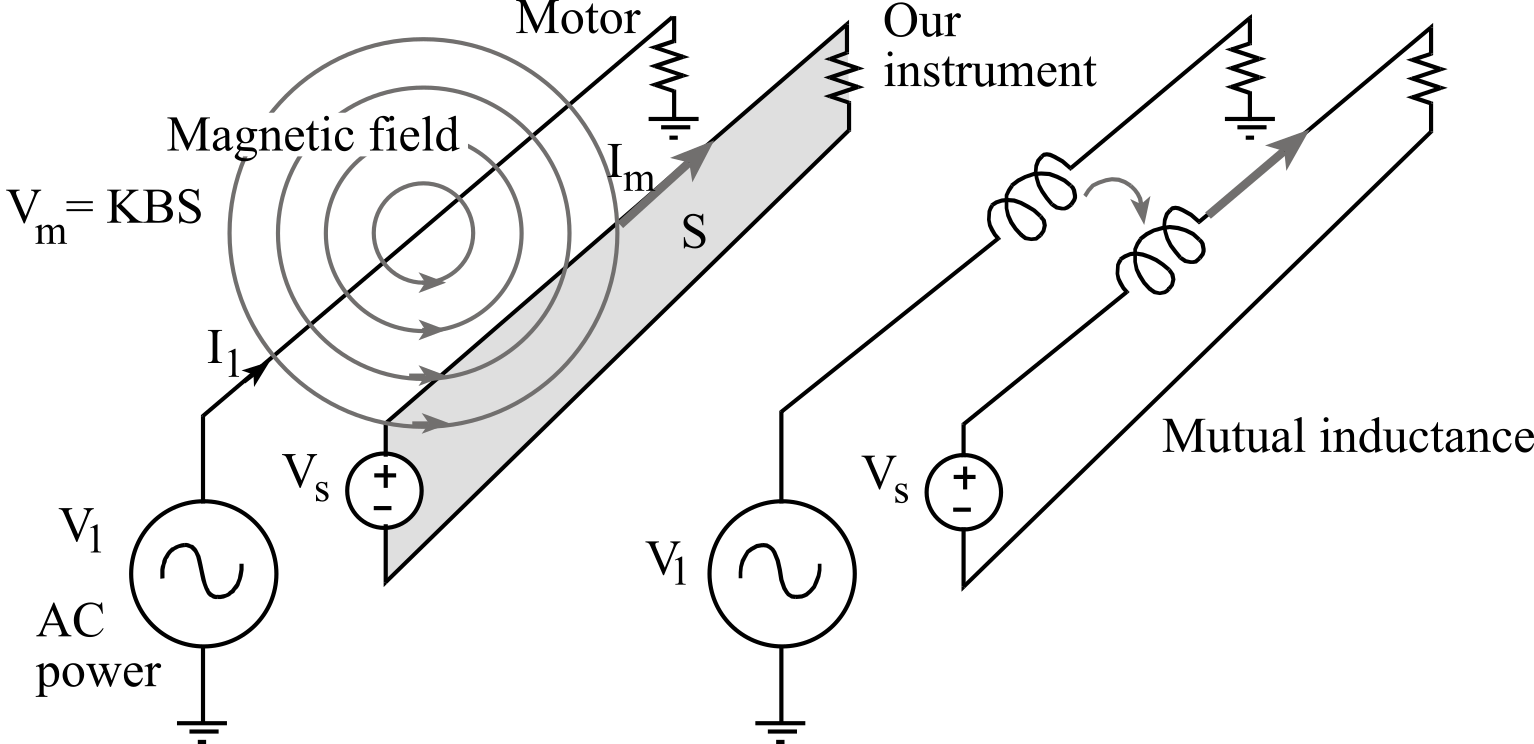
Figure 2.5.2. Magnetic field noise pickup can be modeled as a transformer.
The second way EM fields can be coupled into our circuits is via the electric field. Changing electric fields will capacitively couple into the lead wires. The drawing on the left of Figure 2.5.3 illustrates the physical situation causing electric field pickup. The alternating voltage (V1) will create an electric field. This electric field also traverses near the wires in our circuit (such as the lead wires between the transducer and the instrument box.) This will induce a displacement current (Id) along the wire. We can test for the presence of electric field pickup by placing a shield separating our electronics from the source of the field and observing the magnitude of the noise. The drawing on the right of Figure 2.5.3 illustrates an equivalent circuit we can use to model electric field pickup. Basically, we can model electric fields induced noise as a stray capacitance between an AC voltage and our electronics.
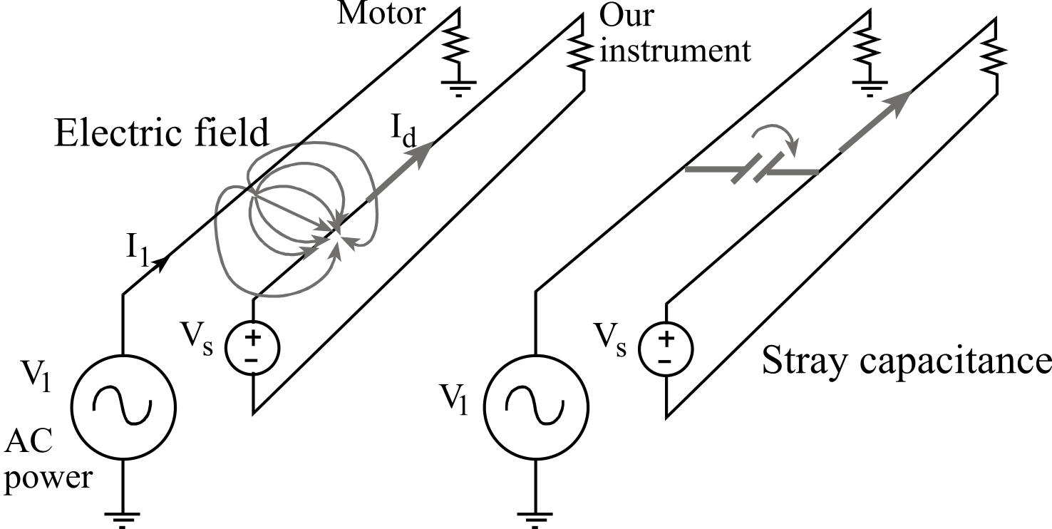
Figure 2.5.3. Electric field noise pickup can be modeled as a stray capacitance.
Observation: Sometimes the EM fields originate from inside the instrument box, such as high frequency digital clocks and switching power supplies.
2.5.3. Techniques to Measure Noise
There are two objectives when measuring noise. The first objective is to classify the type of noise. In particular, we wish to know if the noise is broadband (i.e., all frequencies, like white noise) or does the noise certain specific frequencies (e.g., 60, 120, 180 Hz,... like 60 Hz EM field pickup). The type of noise is of great importance when determining where the noise is coming from. Classifying noise type is essential in developing a strategy for reducing the effect of the noise. The second objective is to quantify the magnitude of the noise. Quantifying the noise is helpful in determining if a change to the system design has increased or decreased the noise. The measurement resolution of many data acquisition systems is limited by noise rather than by ADC precision and software algorithms. For these systems, quantitative noise measurements are an important performance parameter.
Digital voltmeter (DVM) in AC mode. Root-mean-squared (RMS) is defined as the square root of the time-average of the squared voltage (Figure 2.5.1). If the input is constant, fluctuations in the output contain just noise. Because the resistance load is usually constant, squaring the voltage results in a signal proportional to noise power. The averaging calculation gives a measure related to average power, and the square root produces a result with units in volts. RMS noise of a signal can be measured with a DVM using AC mode. Most DVMs in AC mode perform a direct measurement of RMS; hence this method is the most precise. For example, a 3½ digit DVM has a precision of about 11 bits. A calibrated voltmeter in AC mode will be the most accurate quantitative method to measure noise.
Analog oscilloscope. The second method is to connect the signal to an oscilloscope and measure the peak-to-peak noise amplitude, as illustrated in Figure 2.5.4. The crest factor is the ratio of peak value divided by RMS. The peak value is ½ of the peak-to-peak amplitude and can be estimated from the scope tracing. From Table 2.5.2, we see for white noise that the crest factor is about 4, so we can approximate the RMS noise amplitude by dividing the peak-to-peak noise by 8. Because the quantitative assessment of noise with a scope requires visual observation, this method can only be used to approximate the quantitative level of noise. One the other hand, oscilloscope have very high bandwidth, and therefore they are good for classifying high frequency noise. White noise and 1/f noise look random, like the left graph in Figure 2.5.4. For white and 1/f noise, the scope trigger will not be able to capture a repeating waveform. Noise from EM fields on the other hand are repeating and can be triggered by the scope. In fact, the line-trigger setting on the scope can be used specifically to see if the noise is correlated to the 60 Hz 120VAC power line. In particular, 60 Hz noise will trigger when using the line-trigger setting of the scope. The shape of the noise varies depending on the relative strengths of the fundamental and harmonic frequencies. The graph on the right is a periodic wave with a fundamental plus a 50% strength first harmonic.
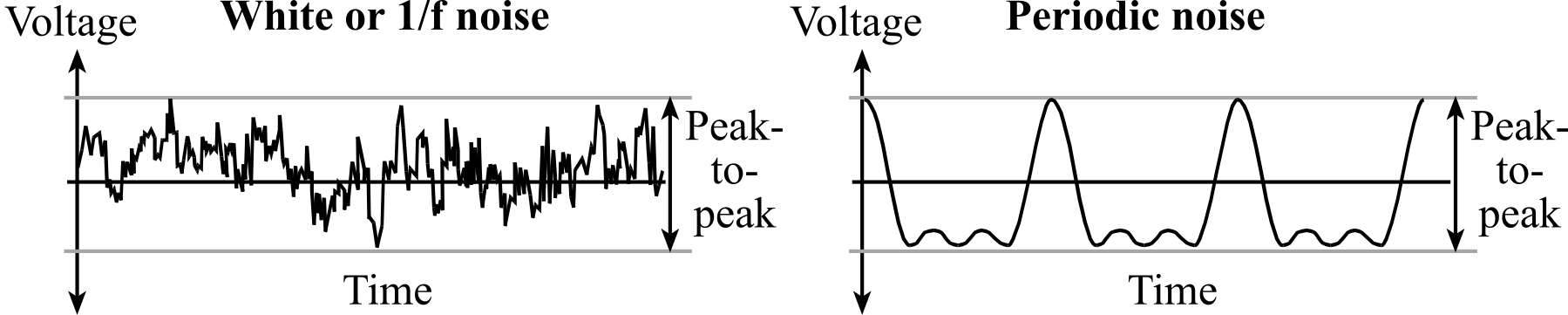
Figure 2.5.4. Quantifying noise my measuring peak-to-peak amplitude.
Spectrum analyzer. The third method uses a spectrum analyzer, which combines a computer, high-speed ADC sampling and the Fast-Fourier-Transform (FFT), as illustrated in Figure 2.5.5. Being able to see the noise in the frequency domain is particularly useful to classify the type of noise. Both 1/f and white noise components exist in a typical analog amplifier, but the amplitude is usually small compared to EM field noise. The 1/f and white noise levels occurring in electronics can be reduced by dropping the temperature or spending more money buying better components. Typically, we see the fundamental and multiple harmonics for EM field noise. For example, 60 Hz noise also includes components at 120, 180, 240 Hz etc.
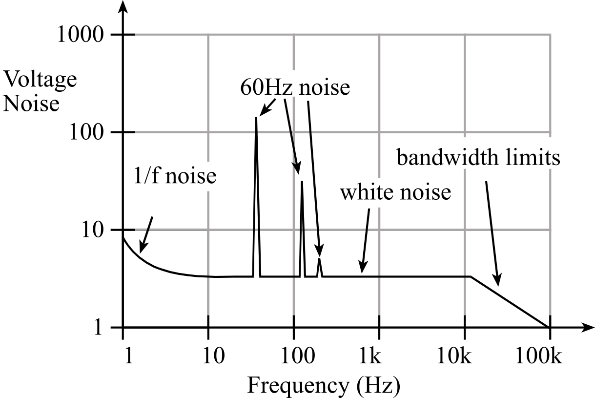
Figure 2.5.5. Classifying noise by measuring the amplitude versus frequency with a spectrum analyzer.
Software. The fourth method is to write software to sample the signal N times with an ADC. Assume the input is constant, so any variability arises from noise. Let Xi be the sampled data. We calculate the signal, AveX, as the average of the sampled input
AveX = (1/N) sum(Xi) for i = 0 to N-1
We calculate the noise, S, as the standard deviation.
S = √((1/(N-1))*sum((Xi- AveX)2 ) for i = 0 to N-1
We calculate SNR as the average/standard deviation AveX/S. There are many definitions for effective number of bits (ENOB). However, one simple definition is
ENOB = log2(AveX/S)
2.5.4. Techniques to Reduce Noise
It is much simpler to reduce noise early in the design process. Conversely, it can be quite expensive to eliminate noise after a system has been built. Therefore, it is important to consider noise at every stage of the development cycle. We can divide noise reduction techniques into three categories. The first category involves reducing noise from the source. You can enclose noisy sources in a grounded metal box. If a cable contains a high frequency noise signal, then that signal could be filtered. Magnetic and electric field strength depends on dI/dt and dV/dt. So whenever possible, you should limit the rise/fall times of noisy signals, as shown in Figure 2.5.6. For example, the square wave on the left will radiate more noise than the smooth signal on the right. When operating a GPIO output pin in 8mA drive mode, we can set the corresponding bit in the SLR register to limit the slew rate on the output.

Figure 2.5.6. Limiting rise/fall times can reduce radiated noise.
Motors have coils to create electromagnets, and noise can be reduced by limiting the dI/dt in the coil. Cables with noisy signals should be twisted together, so the radiated magnetic fields will cancel. These cables should also be shielded to reduce electric field radiation, and this shield should be grounded on both sides.
The second category of noise reduction involves limiting the coupling between the noise source and your system. Whenever possible, maximize the distance between the noisy source and the delicate electronics. All transducer cables should use twisted wire, as shown in Figure 2.5.7.
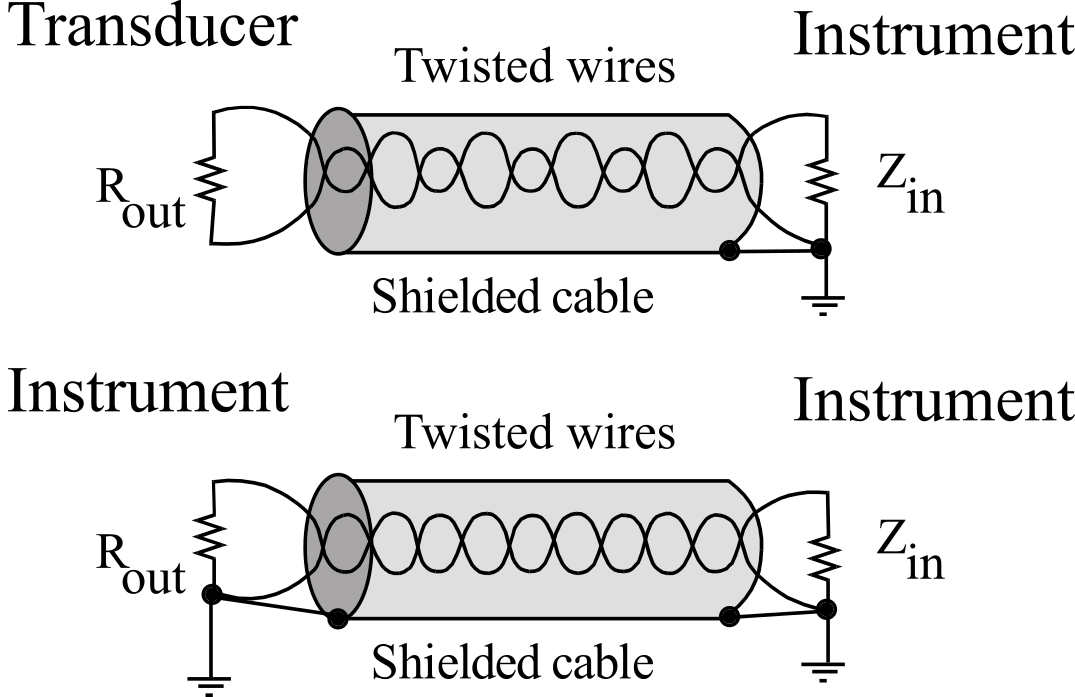
Figure 2.5.7. Proper cabling can reduce noise when connecting to a remote transducer or when connecting two instruments.
For situations where a remote sensor is attached to an instrument, the ground shield should be connected only on the instrument side. If the cable is connected between two instruments, then connect the ground shield on both instruments. For high frequency signals coaxial cable is required. The shield should be electrically insulated to eliminate direct electrical connection to other devices. If noisy signals must exist in the same cable as low-level signals, then separate the two with a ground wire in between. Whenever possible reduce the length of a cable. Similarly minimize the length of leads that extend beyond the ground shield. Place the delicate electronics in a grounded case. You can use optical or transformer isolation circuits to separate the noisy ground from the ground of the delicate electronics.
The last category involves techniques that reduce noise at the receiver. The bandwidth of the system should be as small as possible. You can use an analog low pass filter to reduce the bandwidth, which will also reduce the noise. You can add frequency-reject digital filters to reduce specific noise frequencies like 60, 120, 180 Hz. You should use power supply decoupling capacitors on each chip to reduce the noise coupling from the power supply to the electronics. Figure 2.5.8 illustrates how EM field noise will affect our system. If the cable has twisted wires then Id1 should equal Id2. The input impedance of the amplifier is usually much larger than the source impedance of the signal. Thus, V1-V2 = Rs1 Id1 - Rs2 Id2.
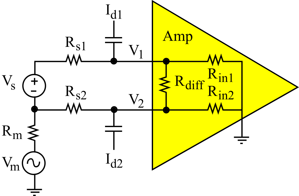
Figure 2.5.8. Capacitively coupled displacement currents.
Some capacitors have a foil wrap surrounding its cylindrical shape. This foil should be grounded. For more information about noise refer to Henry Ott, Noise Reduction Techniques in Electronic Systems, Wiley, 1988 or Ralph Morrison, Grounding and Shielding Techniques, Wiley, 1998.
Observation: Understanding, quantifying, and reducing noise will have a significant impact on the performance of your system.
2.5.5. Central Limit Theorem
A common approach to improving SNR is to take multiple samples and average the results. In fact, most microcontrollers can implement this averaging in hardware. On the TM4C123, we set the ADC0_SAC_R register to n to collect/average 2n samples. The Central Limit Theorem (CLT) describes the result when multiple samples are added together. Consider data as a random variable, which is signal plus noise. To use the CLT, we must assume the noise is independent and identically distributed. As the data are added, their sum tends toward a Gaussian (or Normal) distribution. In other words, as more and more data are added together (averaging), the probability mass function (PMF) of the sum (or average) will tend towards a Gaussian shape. If the noise is zero mean, then the average of the data tends to the true signal, and the standard deviation tends to 0. See Figure 2.5.9
Oversampling: We will sample the ADC faster than we need, and average multiple samples to get one reading. This averaging, called oversampling, will improve signal to noise ratio.
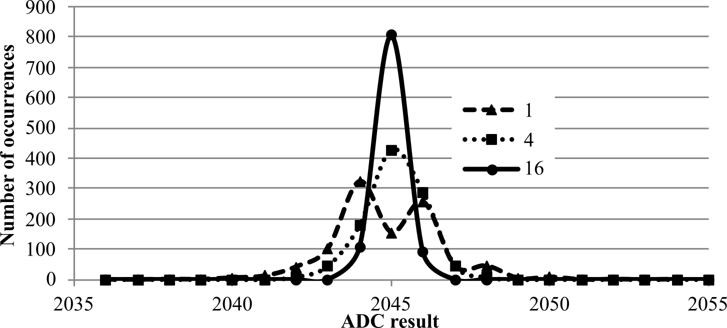
Figure 2.5.9. Probability mass functions showing hardware averaging improves signal to noise ratio.
Observation: Notice the data in Figure 2.5.9 with 1 point (no averaging) has three humps (not normally distributed), but with 16-point averaging there is one symmetric hump (normally distributed).
Video 2.5.1 Central Limit Theorem
2.6. Digital Signal Processing
2.6.1. Multiple Access Circular Queue
A multiple access circular queue (MACQ) is used for implementing digital signal processing (DSP). A MACQ is a fixed length order preserving data structure, see Figure 2.6.1. The source process (ADC sampling software) places information into the MACQ. Once initialized, the MACQ is always full. The oldest data is discarded when the newest data is Put into a MACQ. The sink process can read any of the data from the MACQ. The Read function is non-destructive. This means that the MACQ is not changed by the Read operation.
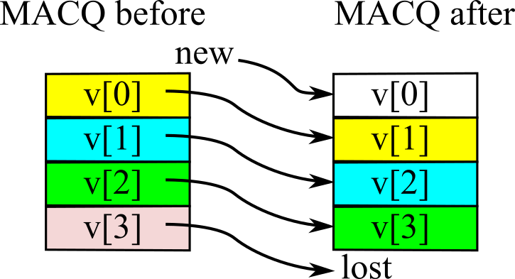
Figure 2.6.1. When data is put into a multiple access circular queue, the oldest data is lost.
For example, consider the problem of weather forecasting as shown in Figure 2.6.2.
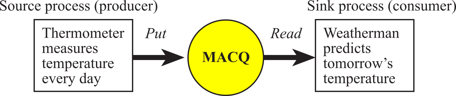
Figure 2.6.2. Application of the multiple access circular queue.
The meteorologist measures the temperature every day at 12 noon and puts the temperature into the MACQ. To predict tomorrow's temperature, she looks at the trend over the last 3 days. Let T(0) be today's temperature, T(1) be yesterday's temperature, etc. We could predict tomorrow's temperature by executing this digital equation, see Program 2.6.1. The low-level ADC code can be found in Section T.2. Details of using the periodic Timer interrupts can be found in Section T.3.
U = (170*T(0)+60*T(1)+36*T(2))/256
int32_t T[3]; // MACQ (C)
int32_t U; // Tomorrow's temperature (C)
void Timer_Handler(void){ uint32_t data;
Debug_HeartBeat0(); // toggle GPIO output
Debug_HeartBeat0(); // toggle GPIO output
data = ADC_In();
T[2] = T[1]; // units of C
T[1] = T[0];
T[0] = Convert(data); // in C
U = (170*T[0]+60*T[1]+36*T[2])<<8; // in C
Debug_HeartBeat0(); // toggle GPIO output
}
Program 2.6.1. Software implementation of weather prediction using a multiple access circular queue.
2.6.2. Averaging Digital Filter
The following function is a low pass digital filter.

Furthermore, if you sample an input at a regular rate, fs, then the following is a digital low pass filter with a cutoff of about fs /2k. This filter calculates the average of the last k samples (for k=16, see Program 2.6.2).

When the MACQ holds many data points it can be implemented using a pointer or index to the newest data, see Figure 2.6.3. In this way, the data need not be shifted each time a new sample is added. The disadvantage of this approach is that address calculation is required during the Read access. For example, we could implement a 16-element averaging filter. More specifically, we will calculate the average of the last 16 samples.
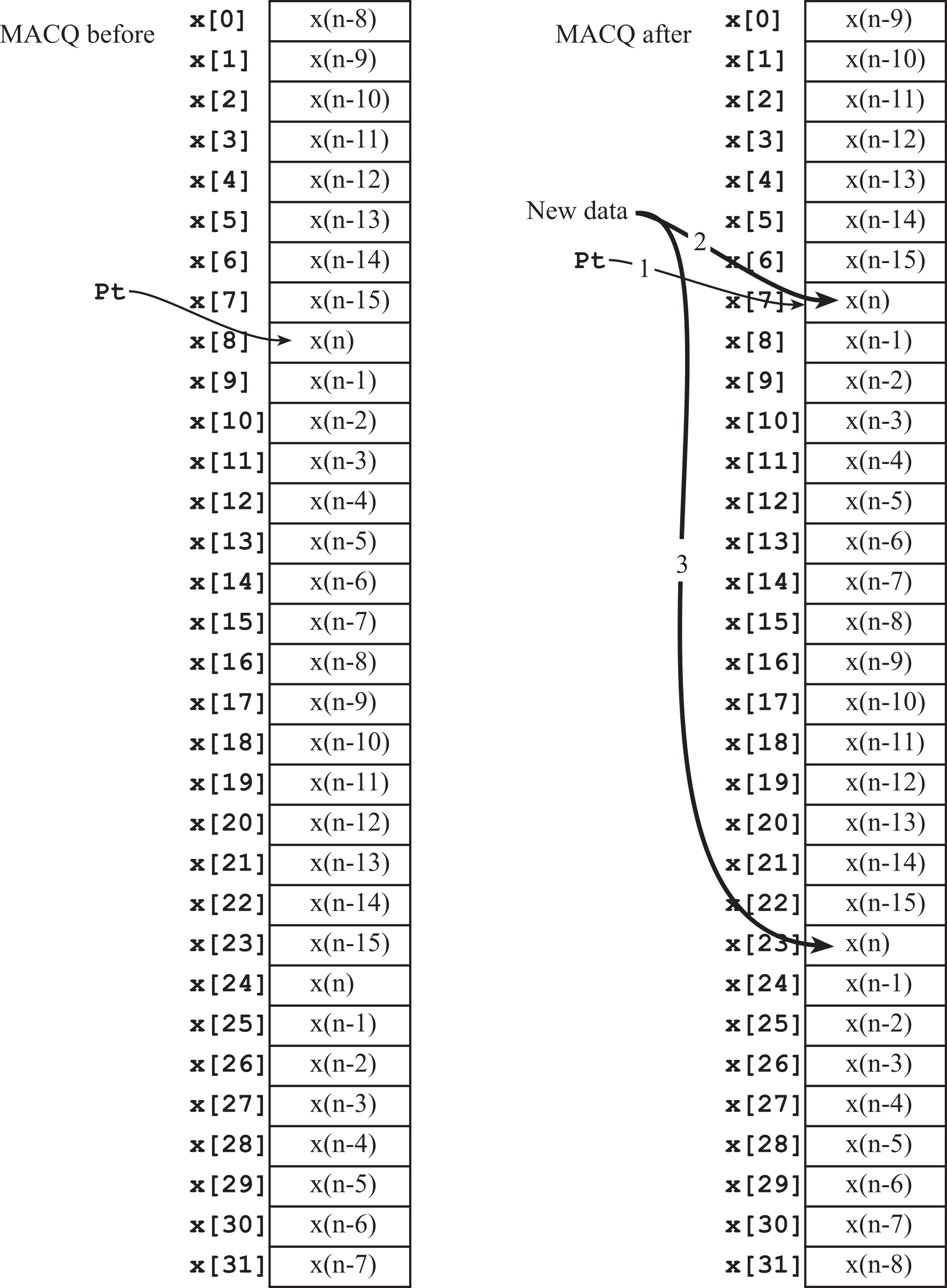
Figure 2.6.3. When data is put into a multiple access circular queue, the oldest data is lost.
Figure 2.6.3 shows the labels x(n), x(n-1),... moving from before to after. Notice however, the data itself does not move. What moves is the significance (or meaning) of the data. The data grows older as time passes. The passage of time is produced by decrementing the pointer. Having two copies of the data makes reading the data faster, because the operation *(Pt+m) never needs wrapping.
Observation: It is possible to implement a pointer-based MACQ that keeps just one copy of the data. Time to access data would be slower, but half as much storage would be needed.
uint32_t Data[32]; // two copies
uint32_t *Pt; // pointer to current
uint32_t Sum; // sum of the last 16 samples
uint32_t y; // output of digital filter
#define fs 1000 // sampling rate in Hz
void LPF_Init(void){
Pt = Data; Sum = 0;
}
// calculate one filter output
// called at sampling rate
// Input: new ADC data
// Output: filter output, DAC data
uint32_t LPF_Calc(uint32_t newdata){
Sum = Sum - *(Pt+16) + newdata; // subtract old, add new
if(Pt == &Data[0]){
Pt = &Data[16]; // wrap
} else{
Pt--; // make room for data
}
*Pt = *(Pt+16) = newdata; // two copies of the new data
return Sum>>4;
}
void SysTick_Handler(void){ uint32_t data;
Debug_HeartBeat0(); // toggle GPIO output pin
Debug_HeartBeat0(); // toggle GPIO output pin
data = ADC0_In()
y = LPF_Calc(data);
Debug_HeartBeat0(); // toggle GPIO output pin
}
Program 2.6.2. Digital low pass filter implemented by averaging the previous 16 samples (cutoff = fs/32).
: If you sample at 1000 Hz, how do you create a digital low pass filter with a cutoff of 10 Hz?
2.6.3. Discrete Derivative
Appendix M.4 develops the math assoiciated with discrete calculus. In this section we present a discrete derivative to illustration how the periodic interrupt, ADC, and MACQ are combined to implement a discrete derivative. The ADC sampling is triggered every 1 ms using a periodic interrupt. x(n) will refer to the current sample, and x(n-1) will be the sample 1 ms ago. There are a couple of ways to implement the discrete time derivative. The simple approach is
d(n) = ( x(n) - x(n-1) )/ Δt
In practice, this first order equation is quite susceptible to noise. An approach generating less noise calculates the derivative using a higher order equation like
d(n) = ( x(n) + 3x(n-1) - 3x(n-2) - x(n-3) )/(6 Δt)
The C implementation of this discrete derivative uses a MACQ. Since Δt is 1 ms, we simply consider the derivative to have units mV/ms and not actually execute the divide by Δt operation. Signed arithmetic is used because the slope may be negative.
int32_t x[4]; // MACQ (mV)
int32_t d; // derivative(mV/ms)
void SysTick_Handler(void){ // runs every 1ms
Debug_HeartBeat0(); // toggle GPIO output pin
Debug_HeartBeat0(); // toggle GPIO output pin
x[3] = x[2]; // shift data
x[2] = x[1]; // units of mV
x[1] = x[0];
x[0] = (3300*ADC0_In())>>12; // in mV
d = (x[0]+3*x[1]-3*x[2]-x[3])/6; // in mV/ms
Fifo_Put(d); // pass to foreground
Debug_HeartBeat0(); // toggle GPIO output pin
}
Program 2.6.3. Software implementation of first derivative using a multiple access circular queue.
Observation: We need to define the variables in Program 2.6.3 as signed because the derivative may be negative.
: Redesign Program 2.6.3 so we can replace the divide by 6 with a shift right by 3.
2.6.4. Sensor Integration
In this section we will discuss strategies for combining data from multiple sensors. For the purposes of this section we will consider three sensors that all measure the distance from the robot to the left wall:
• Tf Luna Time-of-flight sensor
• Sharp GP2Y0A41SK0F IR sensor
• Ping))) Ultrasonic sensor
If we have multiple sensors measuring essentially the same parameter, we can use statistics to combine them into a single value. This approach only works when the sensors yield values with the same units. For example, let d0 be the distance as measured by the time of flight sensor, in mm. Let d1 be the distance as measured by the ultrasonic distance sensor, in mm. Let d2 be the distance as measured by the IR analog distance sensor, in mm. If we had equal confidence in each sensor, we would invoke the Central Limit Theorem and average the three measurements:
d = (d0 + d1 + d2)/3
However, we can use statistics to combine data even when we do not have equal confidence. In statistics, the standard deviation is a measure of confidence. Let σ0, σ1, and σ2 be the standard deviations of the three sensors. In fact, if the probability distribution is normal, the value will be within ±2σ of the mean 95% of the time. In general, we have more confidence in signals with a low standard deviation. The Central Limit Theorem suggests using variance as a weighting factor. We will weight each sensor according to σ-2.
d = ((σ0-2d0 + σ1-2d1 + σ2-2d2)/(σ0-2 + σ1-2 + σ2-2)
Three other strategies will be presented later in the book that make decisions based on sensor measurements that do not necessarily have the same units:
• Finite state machines
• Fuzzy Logic or Buddy Follower Robot using Fuzzy Logic
• Autonomous Racing Robot using Performance Maps
2.7. First In First Out Queue
2.7.1. Classical definition of a FIFO
The first in first out circular queue (FIFO) is quite useful for implementing a buffered I/O interface (Figure 2.7.1). It can be used for both buffered input and buffered output. The order preserving data structure temporarily saves data created by the source (producer) before it is processed by the sink (consumer). The class of FIFOs studied in this section will be statically allocated global structures. Because they are global variables, it means they will exist permanently and can be carefully shared by more than one program. The advantage of using a FIFO structure for a data flow problem is that we can decouple the producer and consumer threads. Without the FIFO we would have to produce 1 piece of data, then process it, produce another piece of data, then process it. With the FIFO, the producer thread can continue to produce data without having to wait for the consumer to finish processing the previous data. This decoupling can significantly improve system performance.
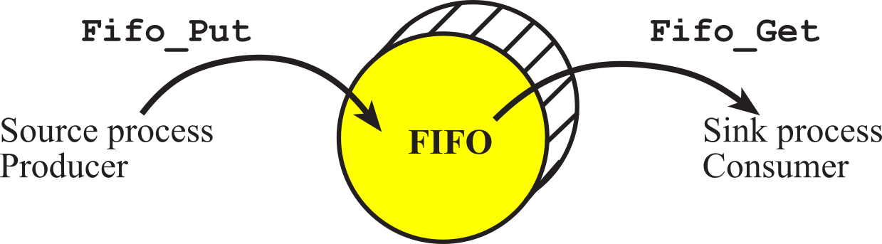
Figure 2.7.1. The FIFO is used to buffer data between the producer and consumer.
You have probably already experienced the convenience of FIFOs. For example, a FIFO is used while streaming audio from the Internet. As sound data are received from the Internet they are put (calls Fifo_Put) in a FIFO. When the sound board needs data it calls Fifo_Get. As long as the FIFO never comes full or empty, the sound is played in a continuous manner. A FIFO is also used when you ask the computer to print a file. Rather than waiting for the actual printing to occur character by character, the print command will put the data in a FIFO. Whenever the printer is free, it will get data from the FIFO. The advantage of the FIFO is it allows you to continue to use your computer while the printing occurs in the background. To implement this magic of background printing we will need interrupts. There are many producer/consumer applications. In Table 2.7.1 the processes on the left are producers that create or input data, while the processes on the right are consumers which process or output data.
|
Source/Producer |
Sink/Consumer |
|
Keyboard input |
Program that interprets |
|
Program with data |
Printer output |
|
Program sends message |
Program receives message |
|
Microphone and ADC |
Program that saves sound data |
|
Program that has sound data |
DAC and speaker |
Table 2.7.1. Producer consumer examples.
The producer puts data into the FIFO. The Fifo_Put operation does not discard information already in the FIFO. If the FIFO is full and the user calls Fifo_Put, the Fifo_Put routine will return a full error signifying the last (newest) data was not properly saved. The sink process removes data from the FIFO. The Fifo_Get routine will modify the FIFO. After a get, the particular information returned from the get routine is no longer saved on the FIFO. If the FIFO is empty and the user tries to get, the Fifo_Get routine will return an empty error signifying no data could be retrieved. The FIFO is order preserving, such that the information is returned by repeated calls to Fifo_Get in the same order as the data was previously saved by calls to Fifo_Put. The causality principle requires data to be put before it can be gotten.
There are many ways to implement a statically-allocated FIFO. We can use either a pointer or an index to access the data in the FIFO. We can use either two pointers (or two indices) or two pointers (or two indices) and a counter. The counter specifies how many entries are currently stored in the FIFO. There are even hardware implementations of FIFO queues. We begin with the two-pointer implementation. It is a little harder to implement, but it does have some advantages over the other implementations.
2.7.2. Two-pointer FIFO implementation
The two-pointer implementation has, of course, two pointers. If we were to have infinite memory, a FIFO implementation is easy (Figure 2.7.2). GetPt points to the data that will be removed by the next call to Fifo_Get, and PutPt points to the empty space where the data will stored by the next call to Fifo_Put, see Program 2.7.1.
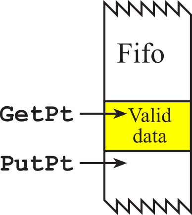
Figure 2.7.2. The FIFO implementation with infinite memory.
int8_t static volatile *PutPt; // put next
int8_t static volatile *GetPt; // get next
int Fifo_Put(int8_t data){ // call by value
*PutPt = data; // Put
PutPt++; // next
return(1); // true if success
}
int Fifo_Get(int8_t *datapt){
*datapt = *GetPt; // return by reference
GetPt++; // next
return(1); // true if success
}
Program 2.7.1. Code fragments showing the basic idea of a FIFO.
There are four modifications that are required to the above subroutines. If the FIFO is full when Fifo_Put is called then the function should return a full error. Similarly, if the FIFO is empty when Fifo_Get is called, then the function should return an empty error. PutPt must be wrapped back up to the top when it reaches the bottom (Figure 2.7.3).
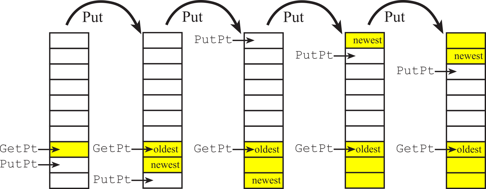
Figure 2.7.3. The FIFO Fifo_Put operation showing the pointer wrap.
The GetPt must also be wrapped back up to the top when it reaches the bottom (Figure 2.7.4).
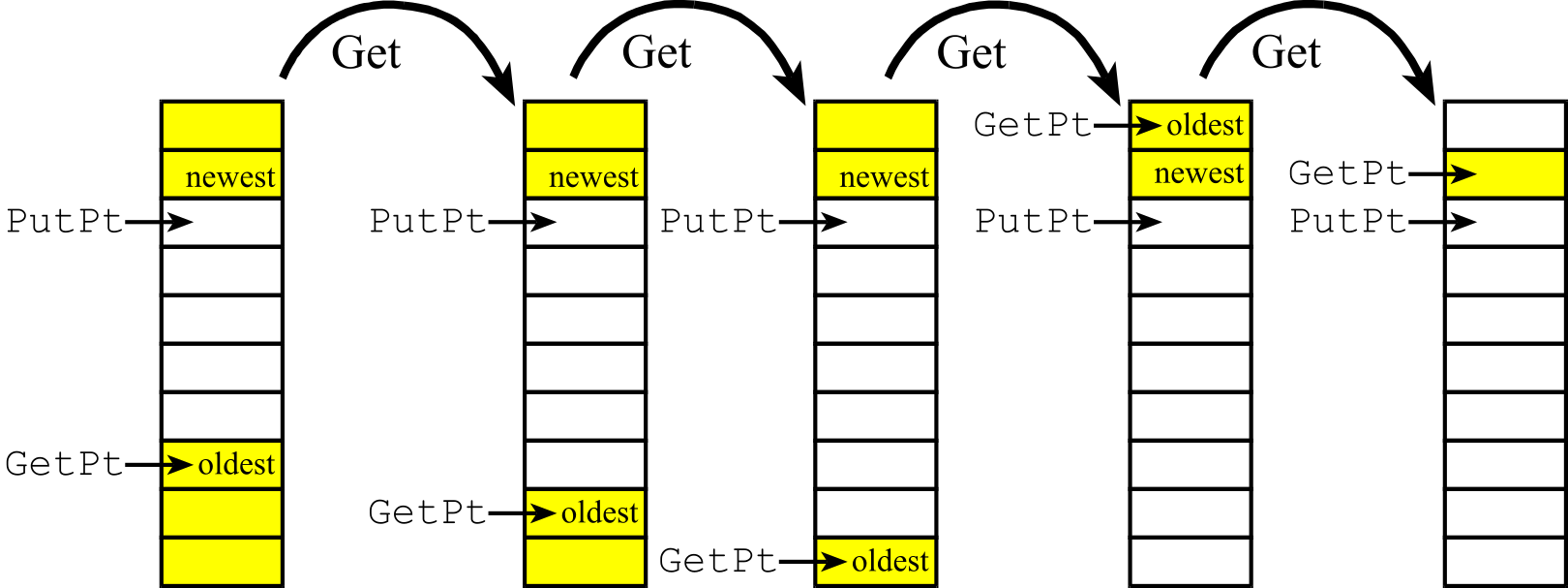
Figure 2.7.4. The FIFO Fifo_Get operation showing the pointer wrap.
There are two mechanisms to determine whether the FIFO is empty or full. A simple method is to implement a counter containing the number of bytes currently stored in the FIFO. Fifo_Get would decrement the counter and Fifo_Put would increment the counter. We will not implement a counter because incrementing and decrementing a counter causes a critical section, meaning the counter could become incorrect when shared in a multithreaded environment. Critical sections will be presented in Section 2.8.
The second method is to prevent the FIFO from being completely full. PutPt equaling GetPt will always mean the FIFO is empty. The implementation of this FIFO module is shown in Program 2.7.2.
#define FIFOSIZE 10 // can be any size
#define FIFOSUCCESS 1
#define FIFOFAIL 0
typedef int8_t Data_t;
Data_t volatile *PutPt; // put next
Data_t volatile *GetPt; // get next
Data_t static Fifo[FIFOSIZE];
// initialize FIFO
void Fifo_Init(void){
PutPt = GetPt = &Fifo[0]; // Empty
}
// add element to FIFO
int Fifo_Put(Data_t data){
Data_t volatile *nextPutPt;
nextPutPt = PutPt+1;
if(nextPutPt == &Fifo[FIFOSIZE]){
nextPutPt = &Fifo[0]; // wrap
}
if(nextPutPt == GetPt){
return(FIFOFAIL); // Failed, FIFO full
}
else{
*(PutPt) = data; // Put
PutPt = nextPutPt; // Success, update
return(FIFOSUCCESS);
}
}
// remove element from FIFO
int Fifo_Get(Data_t *datapt){
if(PutPt == GetPt){
return(FIFOFAIL); // Empty if PutPt=GetPt
}
*datapt = *(GetPt++);
if(GetPt == &Fifo[FIFOSIZE]){
GetPt = &Fifo[0]; // wrap
}
return(FIFOSUCCESS);
}
// number of elements in index FIFO
// 0 to FIFOSIZE-1
uint32_t Fifo_Size(void){
if(RxPutPt < RxGetPt){
return ((uint32_t)(PutPt-GetPt+(FIFOSIZE*sizeof(Data_t)))/sizeof(Data_t));
}
return
((uint32_t)(PutPt-GetPt)/sizeof(Data_t));
}
Program 2.7.2. Two-pointer implementation of a FIFO.
: If FIFOSIZE is 10, why can it only store 9 elements?
For example, if the FIFO had 10 bytes allocated, then the Fifo_Put subroutine would allow a maximum of 9 bytes to be stored. If there were already 9 bytes in the FIFO and another Fifo_Put were called, then the FIFO would not be modified and a full error would be returned. See Figure 2.7.5. In this way, if PutPt equals GetPt at the beginning of Fifo_Get, then the FIFO is empty. Similarly, if PutPt+1 equals GetPt at the beginning of Fifo_Put, then the FIFO is full. Be careful to wrap the PutPt+1 before comparing it to Fifo_Get. This method does not require the length to be stored.
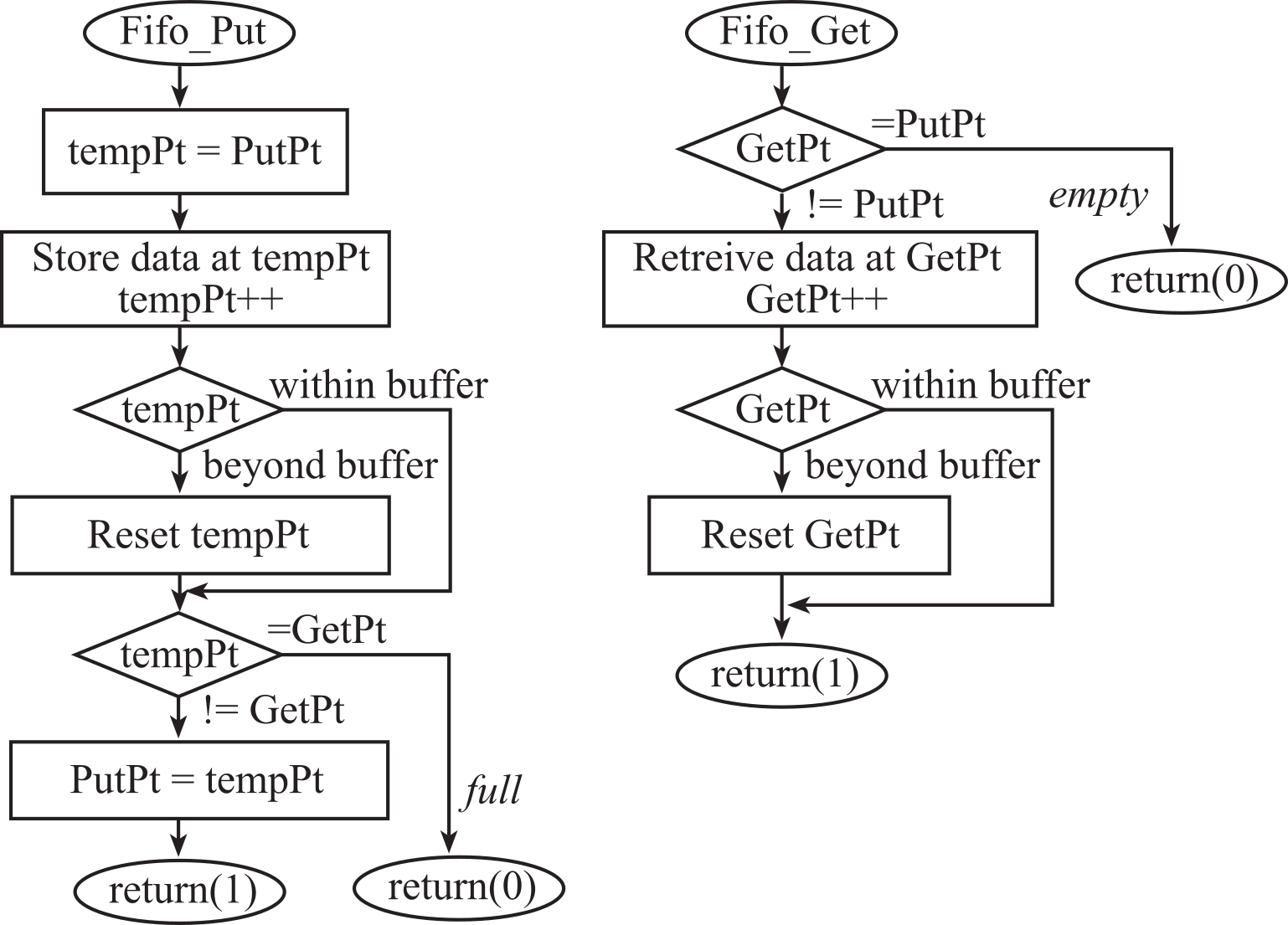
Figure 2.7.5. Flowcharts of the pointer implementation of the FIFO queue.
To check for FIFO full, the Fifo_Put routine creates a temporary put pointer (nextPutPt) to the next place to put. If putting would make the FIFO look empty, then the routine is exited without saving the data. This is why a FIFO with 10 allocated bytes can only hold 9 data bytes. If putting doesn't make the FIFO look empty, then data is saved and nextPutPt is stored into the actual PutPt.
To check for FIFO empty, the Fifo_Get routine in Program 2.7.2 simply checks to see if GetPt equals PutPt. If they match at the start of the routine, then Fifo_Get returns with the "empty" condition signified.
Since Fifo_Put and Fifo_Get have read modify write accesses to global variables they are themselves not reentrant. Similarly, Fifo_Init has a multiple step write access to global variables. Therefore, Fifo_Init is not reentrant.
However, it is safe for Fifo_Put to interrupt Fifo_Get, and it is safe for Fifo_Get to interrupt Fifo_Put. For example, if you have a single thread that calls the Fifo_Get (e.g., the main program) and a single thread that calls the Fifo_Put (e.g., the serial port receive interrupt handler), then this Fifo_Put function can interrupt this Fifo_Get function without loss of data. So in this particular situation, interrupts would not have to be disabled. It would also operate properly if there were a single interrupt thread calling Fifo_Get (e.g., the serial port transmit interrupt handler) and a single thread calling Fifo_Put (e.g., the main program.) On the other hand, if the situation is more general, and multiple threads could call Fifo_Put or multiple threads could call Fifo_Get, then the interrupts would have to be temporarily disabled.
2.7.3. Two index FIFO implementation
The other method to implement a FIFO is to use indices rather than pointers. This FIFO has the restriction that the size must be a power of 2. If FIFOSIZE is 16 and the logic PutI&(FIFOSIZE-1) returns the bottom four bits of the put index. Similarly, the logic GetI&(FIFOSIZE-1) returns the bottom four bits of the get index. Using the bottom bits of the index removes the necessary to check for out of bounds and wrapping.
For more information on this method, see ECE319K ebook Section 8.4
2.7.4. FIFO build macros
When we need multiple FIFOs in our system, we could switch over to C++ and define the FIFO as a class, and then instantiate multiple objects to create the FIFOs. A second approach would be to use a text editor, open the source code containing Program 2.7.2, copy/paste it, and then change names so the functions are unique. A third approach is shown in Programs 2.7.3 and 2.7.4, which defines macros allowing us to create as many FIFOs as we need.
// macro to create a pointer FIFO
#define AddPointerFifo(NAME,SIZE,TYPE,SUCCESS,FAIL) \
TYPE volatile *NAME ## PutPt; \
TYPE volatile *NAME ## GetPt; \
TYPE static NAME ## Fifo [SIZE]; \
void NAME ## Fifo_Init(void){ \
NAME ## PutPt = NAME ## GetPt = &NAME ## Fifo[0]; \
} \
int NAME ## Fifo_Put (TYPE data){ \
TYPE volatile *nextPutPt; \
nextPutPt = NAME ## PutPt + 1; \
if(nextPutPt == &NAME ## Fifo[SIZE]){ \
nextPutPt = &NAME ## Fifo[0]; \
} \
if(nextPutPt == NAME ## GetPt ){ \
return(FAIL); \
} \
else{ \
*( NAME ## PutPt ) = data; \
NAME ## PutPt = nextPutPt; \
return(SUCCESS); \
} \
} \
int NAME ## Fifo_Get (TYPE *datapt){ \
if( NAME ## PutPt == NAME ## GetPt ){ \
return(FAIL); \
} \
*datapt = *( NAME ## GetPt++); \
if( NAME ## GetPt == &NAME ## Fifo[SIZE]){ \
NAME ## GetPt = &NAME ## Fifo[0]; \
} \
return(SUCCESS); \
}
Program 2.7.3. Two-pointer macro implementation of a FIFO.
To create a 20-element FIFO storing unsigned 16-bit
numbers that returns 1 on success and 0 on failure we invoke
AddPointerFifo(Rx, 20, uint16_t, 1, 0)
creating the three functions RxFifo_Init(),
RxFifo_Get(), and RxFifo_Put().
Program 2.7.4 is a macro allowing us to create two-index FIFOs.
// macro to create an index FIFO
#define AddIndexFifo(NAME,SIZE,TYPE,SUCCESS,FAIL) \
uint32_t volatile NAME ## PutI; \
uint32_t volatile NAME ## GetI; \
TYPE static NAME ## Fifo [SIZE]; \
void NAME ## Fifo_Init(void){ \
NAME ## PutI = NAME ## GetI = 0; \
} \
int NAME ## Fifo_Put (TYPE data){ \
if(( NAME ## PutI - NAME ## GetI ) & ~(SIZE-1)){ \
return(FAIL); \
} \
NAME ## Fifo[ NAME ## PutI &(SIZE-1)] = data; \
NAME ## PutI ## ++; \
return(SUCCESS); \
} \
int NAME ## Fifo_Get (TYPE *datapt){ \
if( NAME ## PutI == NAME ## GetI ){ \
return(FAIL); \
} \
*datapt = NAME ## Fifo[ NAME ## GetI &(SIZE-1)]; \
NAME ## GetI++; \
return(SUCCESS); \
} \
uint16_t NAME ## Fifo_Size (void){ \
return ((uint16_t)( NAME ## PutI - NAME ## GetI )); \
}
Program 2.7.4. Macro implementation of a two-index FIFO. The size must be a power of two.
To create a 32-element FIFO storing signed 32-bit numbers
that returns 0 on success and 1 on failure we invoke
AddIndexFifo(Tx, 32, int32_t, 0, 1)
creating the three functions TxFifo_Init(),
TxFifo_Get(), and TxFifo_Put().
: Show C code to create a FIFO called CAN1. It stores 8-bit unsigned bytes and must be able to store up to 99 elements.
: Show C code to create a FIFO called F1. It stores 16-bit signed halfwords and must be able to store up to 255 elements.
2.7.5. Little's Theorem
In this section we introduce some general theory about queues. Let N be the average number of data packets in the queue plus the one data packet currently being processed by the consumer. Basically, N is the average number of packets in the system. Let l be the average arrival rate in packets per second (pps). Let R be the average response time of a packet, which includes the time waiting in the queue plus the time for the consumer to process the packet. Little's Theorem states
N = lR
As long as the system is stable, this result is not influenced by the probability distribution of the producer, the probability distribution of the consumer or the service order. Let S be the mean service time for a packet. Thus, C=1/S is defined as the system capacity (pps). Stable in this context means the packet arrival rate is less than the system capacity (l<C). This means, in most cases, the queue length can be chosen so the queue never fills, and no data are lost. In this case, the arrival rate l is equal to the output rate T, or throughput of the system. We can use Little's Theorem to estimate average response time,
R = N/T
In general, we want T to be high and R to be low. To handle these two conflicting goals, we develop the concept of a power metric for the queue. We can define utilization factor as the throughput divided by the capacity, which is a normalized throughput,
U = T/C
U defines the loading of the queue, because it is the ratio of throughput divided by capacity. We can define normalized mean response time, R/S. We next define power metric P as utilization factor divided by normalized mean response time,
P = U/(R/S) = (T*S)/(R/S)
Substituting Little's Theorem (R=N/T), we can write
P = U2/N
The goal of the operating system is to maximize P.
2.8. Critical Sections
In general, if two threads access the same global memory and one of the accesses is a write, then there is a causal dependency between the threads. This means, the execution order may affect the outcome. Shared global variables are very important in multithreaded systems because they are required to pass data between threads, but they exhibit complex behavior, and it is hard to find bugs that result with their use.
A program segment is reentrant if it can be concurrently executed by two (or more) threads. To implement reentrant software, we place variables in registers or on the stack and avoid storing into global memory variables. When writing in assembly, we use registers, or the stack for parameter passing to create reentrant subroutines. Typically, each thread will have its own set of registers and stack. A nonreentrant subroutine will have a section of code called a vulnerable window or critical section. An error occurs if
1) One thread calls the
function in question
2) It is executing in the
critical section when interrupted by a second thread
3) The second thread calls
the same function.
There are several scenarios that can happen next. In the most common scenario, the second thread is allowed to complete the execution of the function, control is then returned to the first thread, and the first thread finishes the function. This first scenario is the usual case with interrupt programming. In the second scenario, the second thread executes part of the critical section, is interrupted and then re-entered by a third thread, the third thread finishes, the control is returned to the second thread and it finishes, lastly the control is returned to the first thread and it finishes. This second scenario can happen in interrupt programming if the second interrupt has higher priority than the first. A critical section may exist when two different functions that access and modify the same memory-resident data structure.
Program 2.8.1 shows a C function, and the assembly code generated by the ARM Keil uVision compiler. The function is nonreentrant because of the read-modify-write nonatomic access to the global variable, num. The "could be bad" mark spots in the code that might cause an error if the interrupt were to occur here. These three spots are defined as the critical section.
|
num SPACE 4 Count LDR r0,[pc,#116] ; R0= &num LDR r0,[r0,#0x00] ; R0=num ;could be bad if interrupt occurs here ADDS r0,r0,#1 ;could be bad if interrupt occurs here LDR r1,[pc,#108] ; R1=&num ;could be bad if interrupt occurs here STR r0,[r1,#0x00] ; update num ;*******end of critical section*** BX lr ptr DCD num |
uint32_t volatile num; void Count(void){ num = num + 1; } |
Program 2.8.1. This function is nonreentrant because of the read-modify-write access to a global.
Assume there are two concurrent threads (the main program and a background ISR) that both call this function. Concurrent means that both threads are ready to run. Because there is only one computer, exactly one thread will be running at a time. Typically, the operating system switches execution control back and forth using interrupts. There are three places marked "could be bad" in the assembly code at which if an interrupt were to occur and the ISR called the same function, the end result would be num would be incremented only once, even though the function was called twice. Assume for this example num is initially 100. An error occurs if:
1. The main program
calls Count
2. The main executes LDR r0,[r0,#0x00] making R0 = 100
3. Main program is halted by an interrupt and starts the ISR
4. The ISR calls Count Executes num=num+1; making num equal to 101
5. The returns back to the main program
R0 is back to its
original value of 100
6. The main program
finished the function (adding 1 to R0),
making num
equal to 101
An atomic operation is one that once started is guaranteed to finish. In most computers, once an instruction has begun, the instruction must be finished before the computer can process an interrupt. Nonreentrant code has the following required properties
1) nonatomic sequences,
2) writes and
3) global variables.
We will classify I/O ports as global variables for the consideration of critical sections. We will group registers into the same category as local variables because each thread will have its own registers and stack.
The first critical section is the read-modify-write sequence:
1) The software reads the global variable producing a copy of the data
2) The software modifies the copy (original variable is still unmodified)
3) The software writes the modification back into the global variable.
In the second critical section, we have a write followed by read, where the global variable is used for temporary storage:
1) The software writes to the global variable (only copy of the information)
2) The software reads from the global variable expecting the original data to be there.
In the third critical section, we have a non-atomic multi-step write to a global variable:
1) The software writes part of the new value to a global variable
2) The software writes the rest of the new value to a global variable.
Observation: When considering reentrant software and vulnerable windows we classify accesses to I/O ports the same as accesses to global variables.
Observation: Sometimes we store temporary information in global variables out of laziness. This practice is to be discouraged because it wastes memory and may cause a critical section.
Sometimes, we can have a critical section between two different software functions (one function called by one thread, and another function called by a different thread). In addition to above three cases, a non-atomic multi-step read will be critical when paired with a multi-step write. For example, assume a data structure has multiple components (e.g., hours, minutes, and seconds). In this case, the write to the data structure will be atomic because it occurs in a high priority ISR. The critical section exists in the foreground between steps 1 and 3. In this case, a critical section exists even though no software has been reentered.
|
Foreground thread 1) The main reads some of the data
3) The main reads the rest of the data |
Background thread
2) ISR writes to the data structure |
In a similar case, a non-atomic multi-step write will be critical when paired with a multi-step read. Again, assume a data structure has multiple components. In this case, the read from the data structure will be atomic because it occurs in a high priority ISR. The critical section exists in the foreground between steps 1 and 3.
|
Foreground thread 1) The main writes some of the data
3) The main writes the rest of the data |
Background thread
2) ISR reads from the data structure |
If critical sections do exist, we can either eliminate it by removing the access to the global variable or implement mutual exclusion, which simply means only one thread at a time is allowed to execute in the critical section. In general, if we can eliminate the global variables, then the subroutine becomes reentrant. Without global variables there are no "vulnerable" windows because each thread has its own registers and stack. Sometimes one must access global memory to implement the desired function. Remember that all I/O ports are considered global. Furthermore, global variables are necessary to pass data between threads. Software in Program 2.8.2 can be used to disable and enable interrupts
|
// TM4C123 |
// MSPM0G3507 |
Program 2.8.2. Assembly functions needed for interrupt enabling and disabling.
A simple way to implement mutual exclusion is to disable interrupts while executing the critical section. It is important to disable interrupts for as short a time as possible, to minimize the effect on the dynamic performance of the other threads. While we are running with interrupts disabled, time-critical events like power failure and danger warnings cannot be processed. We will add the assembly code of Program 2.8.2 to the Startup.s file in our projects that use interrupts. Program 5.4 illustrates how to implement mutual exclusion and eliminate the critical section.
uint32_t volatile num;
void Count(void){
DisableInterrupts(); // make it atomic
num = num + 1;
EnableInterrupts();
}
Program 2.8.3. This function is reentrant because of the read-modify-write access to the global is atomic.
: There is a bug in the approach of Program 2.8.3 when critical sections are nested. For example, one function with a critical section calls a second function that also has a critical section. What bug would happen if you added disable interrupt at the beginning and a reenable interrupt at the end of each critical section?
Another category of timing-dependent bugs, like critical sections, is called a race condition. A race condition occurs in a multi-threaded environment when there is a causal dependency between two or more threads. In other words, different behavior occurs depending on the order of execution of two threads.
Example 1) Thread-1 initializes Port B bits 3-0 by writing 0x0F to the enable register. Thread-2 initializes Port B bits 6- 4 by writing 0x70 to the same enable register. If Thread-1 runs first, and Thread-2 runs second, then Port B bits 3-0 will be disabled. Conversely, if Thread-2 runs first, and Thread-1 runs second, then Port B bits 6-4 will be disabled. This is a race condition caused by unfriendly code. The solution to this problem is to write the two initializations in a friendly manner, and make both initializations atomic. Initializations should be run at the beginning of the program before interrupts are enabled, this way all initializations are atomic.
|
Thread-1 Sets Port B enable to 0x0F
|
Thread-2 Sets Port B enable to 0x70
|
Example 2) Assume two threads are trying to get data from the same input device. Both call the function UART_InChar. When data arrives at the input, the thread that executes first will capture the data. The thread that executes second will not get this data, but will have to wait for the next UART input.
|
Thread-1 Data1 = UART_InChar();
|
Thread-2 Data2 = UART_InChar();
|
2.9. Lab 2
Lab 2 for this course can be downloaded from this link Lab02.docx
Each lab also has a report Lab02Report.docx
This work is based on the course ECE445L
taught at the University of Texas at Austin. This course was developed by Jonathan Valvano, Mark McDermott, and Bill Bard.
Reprinted with approval from Embedded Systems: Real-Time Interfacing to ARM Cortex-M Microcontrollers, ISBN-13: 978-1463590154

Embedded Systems: Real-Time Interfacing to ARM Cortex-M Microcontrollers by Jonathan Valvano is
licensed under a Creative
Commons
Attribution-NonCommercial-NoDerivatives 4.0 International License.