Chapter 7. System Design
Table of Contents:
- 7.1. I/O Device Drivers
- 7.1.1. Layered Software
- 7.1.2. Board Support Package
- 7.1.3. Serial Port Driver
- 7.1.4. Abstract Output Device Driver
- 7.2. Design Paradigms
- 7.3. Design for Manufacturability
- 7.4. Low-Power Design
- 7.5. Design for Testability
- 7.6. Lab 7. System Design
Chapters 1 to 6 of this book have presented embedded systems from an interfacing or component level. The remaining chapters will focus on systems level design.
7.1. I/O Device Drivers
In this section we demonstrate modular programming as an effective way to organize our I/O software. There are three reasons for forming modules. First, functional abstraction allows us to reuse a software module from multiple locations. Second, complexity abstraction allows us to divide a highly complex system into smaller less complicated components. The third reason is portability. If we create modules for the I/O devices then we can isolate the rest of the system from the hardware details. Portability will be enhanced when we create a device driver or board support package.
7.1.1. Layered Software
As the size and complexity of our software systems increase, we learn to anticipate the changes that our software must undergo in the future. We can expect to redesign our system to run on new and more powerful hardware platforms. A similar expectation is that better algorithms may become available. The objective of this section is to use a layered software approach to facilitate these types of changes.
Figure 7.1.1 shows two ways to draw a call graph that visualizes software layers. Figure 7.1.1 shows only one module at each layer, but a complex system might have multiple modules at each layer. A function in a layer can call a function within the same module, or it can call a public function in a module of the same or lower layer. Some layered systems restrict the calls only to modules in the most adjacent layer below it. If we place all the functions that access the I/O hardware in the bottom most layer, we can call this layer a hardware abstraction layer (HAL). This bottom-most layer can also be called a board support package (BSP) if I/O devices are referenced in an abstract manner. Each middle layer of modules only calls lower-level modules, but not modules at a higher level. Usually, the top layer consists of the main program. In a multi-threaded environment, there can be multiple main programs at the top-most level, but for now assume there is only one main program.
An example of a layered system is Transmission Control Protocol/Internet Protocol (TCP/IP), which consists of at least four distinct layers: application (http, telnet, SMTP, FTP), transport (UDP, TCP), internet (IP, ICMP, IGMP), and network layers (Ethernet).
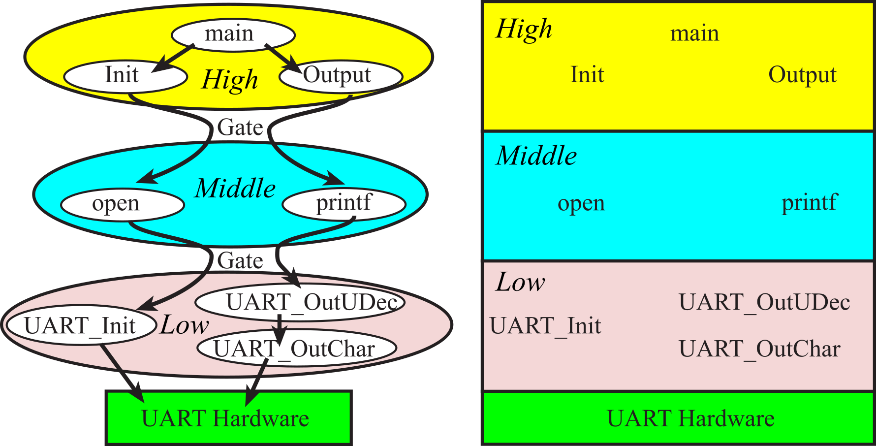
Figure 7.1.1. A layered approach to interfacing a printer. The bottom layer is the BSP.
To develop a layered software system we begin with a modular system. The main advantage of layered software is the ability to separate the modules into groups or layers such that one layer may be replaced without affecting the other layers. For example, you could change which microcontroller you are using, by modifying the low level without any changes to the other levels. Figure 7.1.1 depicts a layered implementation of a printer interface. In a similar way, you could replace the printer with a solid-state disk by replacing just the middle and lower layers. If we were to employ buffering and/or data compression to enhance communication bandwidth, then these algorithms would be added to the middle level. A layered system should allow you to change the implementation of one layer without requiring redesign of the other layers.
A gate is used to connect one layer to the next. Another name for this gate is application program interface or API. The gates provide a mechanism to link the layers. Because the size of the software on an embedded system is small, it is possible and appropriate to implement a layered system using standard function calls by simply compiling and linking all software together. We create a header file with prototypes to public functions. The following rules apply to layered software systems:
1. A module may make a simple call to other modules in the same layer.
2. A module may make a call to a lower level module only by using the gate.
3. A module may not directly access any function or variable in another layer without going through the gate.
4. A module may not call a higher level routine.
5. A module may not modify the vector address of another level's handler(s).
6. (optional) A module may not call farther down than the immediately adjacent lower level.
7. (optional) All I/O hardware access is grouped in the lowest level.
8. (optional) All user interface I/O is grouped in the highest level
unless it is the purpose of the module itself to do such I/O.
The purpose of rule 6 is to allow modifications at the low layer to not affect operation at the highest layer. On the other hand, for efficiency reasons you may wish to allow module calls further down than the immediately adjacent lower layer. To get the full advantage of layered software, it is critical to design functionally complete interfaces between the layers. The interface should support all current functions as well as provide for future expansions.
7.1.2. Board Support Package
A device driver or firmware consists of software routines that provide the functionality of an I/O device. A device driver usually does not hide what type of I/O module it is. For example, in Section 7.1.3, we consider a device driver for a serial port. A board support package is like a device driver, except that there is more of an attempt to hide the details of the I/O device. A board support package provides a higher level of abstraction than a regular device driver. The driver consists of the interface routines that the operating system or software developer's program calls to perform I/O operations as well as the low-level routines that configure the I/O device and perform the actual input/output. The issue of the separation of policies from mechanisms is very important in device driver design. The policies of a driver include the list of functions and the overall expected results. In particular, the policies can be summarized by the interface routines that the OS or software developer can call to access the device. The mechanisms of the device driver include the specific hardware and low-level software that perform the I/O. As an example, consider the wide variety of mass storage devices that are available. Flash EEPROM hard drive, battery-backed RAM hard drive, magnetic hard drive, optical hard drive, ferroelectric RAM hard drive, and even a network can be used to save and recall data files. A simple mass storage system might have the following C-level interface functions, as explained in the following prototypes (in each case the functions return 0 if successful and an error code if the operation fails:
int eFile_Init(void); // initialize file system
int eFile_Create(char name[]); // create new file, make it empty
int eFile_WOpen(char name[]); // open a file for writing
int eFile_Write(int8_t data); // stream data into open file
int eFile_WClose(void); // close the file for writing
int eFile_ROpen(char name[]); // open a file for reading
int eFile_ReadNext(int8_t *pt); // stream data out of open file
int eFile_RClose(void); // close the file for reading
int eFile_Delete(char name[]); // remove this file
Building a hardware abstraction layer (HAL) is the same idea as separation of policies from mechanisms. In the above file example, a HAL or BSP would treat all the potential mass storage devices through the same software interface. Another example of this abstraction is the way some computers treat pictures on the video screen and pictures printed on the printer. With the abstraction layer, the software developer's program draws lines and colors by passing the data in a standard format to the device driver, and the OS redirects the information to the video graphics board or color printer as appropriate. This layered approach allows one to mix and match hardware and software components but does suffer some overhead and inefficiency.
Low-level device drivers normally exist in the Basic Input/Output System (BIOS) ROM and have direct access to the hardware. They provide the interface between the hardware and the rest of the software. Good low-level device drivers allow:
1. New hardware to be installed;
2. New algorithms to be implemented
a. Synchronization with busy wait, interrupts, or DMA,
b. Error detection and recovery methods
c. Enhancements like automatic data compression
3. Higher level features to be built on top of the low level
a. OS features like blocking semaphores
b. Additional features like function keys
and still maintain the same software interface. In larger systems like the personal computer (PC), the low-level I/O software is compiled and burned in ROM separate from the code that will call it, it makes sense to implement the device drivers as software interrupts or traps, e.g., the SVC instruction, and specify the calling sequence language-independent according to AAPCS. We define the "client programmer" as the software developer that will use the device driver. In embedded systems like we use, it is appropriate to provide device.h and device.c files that the client programmer can compile with their application. In a commercial setting, you may be able to deliver to the client only the device.h together with the object file. Linking is the process of resolving addresses to code and programs that have been complied separately. In this way, the routines can be called from any program without requiring complicated linking. In other words, when the device driver is implemented with a software interrupt, the linking occurs at run time through the vector address of the software interrupt. In our embedded system however, the linking will be static occurring at the time of compilation.
7.1.3. Serial Port Driver
The concept of a device driver can be illustrated with the following design of a serial port device driver. In this section, the contents of the header file (UART.h) will be presented, and the implementations can be found in the starter projects for the book. and explained in Appendix T.4. The device driver software is grouped into four categories. Protected items can only be directly accessed by the device driver itself, and public items can be accessed by other modules.
1. Data structures: static (permanently allocated with private scope) The first component of a device driver includes data structures. To be static means only programs within the driver itself may directly access these variables. If the user of the device driver (e.g., a client) needs to read or write to these variables, then the driver will include public functions that allow appropriate read/write functions. One example of a static variable might be an OpenFlag, which is true if the serial port has been properly initialized. static used in this way makes the variable private to the file, but does have permanent allocation. If the implementation uses interrupts, then it will need a FIFO queue, defined with private scope.
int static OpenFlag = 0; // true if
driver has been initialized
2. Initialization routines (public, called by the client once in the beginning) The second component of a device driver includes the public functions used to initialize the device. To be public means the user of this driver can call these functions directly. A prototype to public functions will be included in the header file (UART.h). The names of public functions will begin with UART_. The purpose of this function is to initialize the UART hardware.
//------------UART_Init------------
// Initialize Serial port UART
// Input: none
// Output: none
void UART_Init(void);
3. Regular I/O calls (public, called by client to perform I/O) The third component of a device driver consists of the public functions used to perform input/output with the device. Because these functions are public, prototypes will be included in the header file (UART.h). The input functions are grouped, followed by the output functions.
//------------UART_InChar------------
// Wait for new serial port input
// Input: none
// Output: ASCII code for key typed
char UART_InChar(void);
//------------UART_InString------------
// Wait for a sequence of serial port input
// Input: maxSize is the maximum number of characters to look for
// Output: Null-terminated string in buffer
void UART_InString(char *buffer, uint16_t maxSize);
//------------UART_InUDec------------
// InUDec accepts ASCII input in unsigned decimal format
// and converts to a 32-bit unsigned number (0 to 4294967295)
// Input: none
// Output: 32-bit unsigned number
uint32_t UART_InUDec(void);
//------------UART_OutChar------------
// Output 8-bit to serial port
// Input: letter is an 8-bit ASCII character to be transferred
// Output: none
void UART_OutChar(char letter);
//------------UART_OutString------------
// Output String (NULL termination)
// Input: pointer to a NULL-terminated string to be transferred
// Output: none
void UART_OutString(char *buffer);
//------------UART_OutUDec------------
// Output a 32-bit number in unsigned decimal format
// Input: 32-bit number to be transferred
// Output: none
// Variable format 1-10 digits with no space before or after
void UART_OutUDec(uint32_t number);
4. Support software (private) The last component of a device driver consists of private functions. Again, if interrupt synchronization were to be used, then a set of FIFO functions will be needed. Because these functions are private, prototypes will not be included in the header file (UART.h). We place helper functions and interrupt service routines in the category.
Notice that this UART example implements a layered approach, like Figure 7.1.1. The low-level functions provide the mechanisms and are protected (hidden) from the client programmer. The high-level functions provide the policies and are accessible (public) to the client. When the device driver software is separated into UART.h and UART.c files, you need to pay careful attention as to how many details you place in the UART.h file. A good device driver separates the policy (overall operation, how it is called, what it returns, what it does, etc.) from the implementation (access to hardware, how it works, etc.) In general, you place the policies in the UART.h file (to be read by the client) and the implementations in the UART.c file (to be read by you and your coworkers). Think of it this way: if you were to write commercial software that you wished to sell for profit and you delivered the UART.h file and its compiled object file, how little information could you place in the UART.h file and still have the software system be fully functional. In summary, the policies will be public, and the implementations will be private.
Observation: A layered approach to I/O programming makes it easier for you to upgrade to newer technology.
Observation: A layered approach to I/O programming allows you to do concurrent development.
7.1.4. Abstract Output Device Driver
In the UART driver shown in the previous section, the routines clearly involve a UART. Another approach to I/O is to provide a high-level abstraction in such a way that the I/O device itself is hidden from the user. One example of this abstraction is the standard printf feature to which most C programmers are accustomed. For the TM4C123 and MSPM0 LaunchPad boards, we can send output to the PC using UART0, to a ST7735 color graphics LCD using SPI, or to a low-cost SSD1306 OLED using I2C. Even though all these displays are quite different, they all behave in a similar fashion.
In C with the Keil compiler, we can specify the output stream used by printf by writing a fputc function. The fputc function is a private and implemented inside the driver. It sends characters to the display and manages the cursor, tab, line feed and carriage return functionalities. The user controls the display by calling the following five public functions.
void Output_Init(void); // Initializes the display interface.
void Output_Clear(void); // Clears the display
void Output_Off(void); // Turns off the display
void Output_On(void); // Turns on the display
void Output_Color(uint32_t newColor); // Set color
of future output
The user performs output by calling printf. This abstraction clearly separates what it does (output information) from how it works (sends pixel data to the display over UART, SSI, or I2C). In these examples all output is sent to the display; however, we could modify the fputc function and redirect the output stream to other devices such as the USB, Ethernet, or disk. For the TM4C boards, implementation of printf for both Keil and CCS can be found in projects ST7735_4C123, SSD1306_4C123, Printf_Nokia_4C123, and Printf_UART_4C123, see starter projects for the book
7.2. Design Paradigms
Abstraction is when we define a complex problem with a set of basic abstract principles. If we can construct our software system using these building blocks, then we have a better understanding of the problem. This is because we can separate what we are doing from the details of how we are getting it done. This separation also makes it easier to optimize. It provides proof of the correct function and simplifies both extensions and customization.
A well-defined model or framework is used to solve our problem. The three advantages of abstraction are 1) it can be faster to develop because a lot of the building blocks preexist; 2) it is easier to debug (prove correct) because it separates conceptual issues from implementation; and 3) it is easier to change.
7.2.1. Finite State Machines
A good example of abstraction is the Finite State Machine (FSM) implementations. The abstract principles of FSM development are the inputs, outputs, states, and state transitions. If we can take a complex problem and map it into an FSM model, then we can solve it with simple FSM software tools. Our FSM software implementation will be easy to understand, debug, and modify. Other examples of software abstraction include Proportional Integral Derivative digital controllers, fuzzy logic digital controllers, neural networks, and linear systems of differential equations (e.g., PSPICE.) In each case, the problem is mapped into a well-defined model with a set of abstract yet powerful rules. Then, the software solution is a matter of implementing the rules of the model.
Linked lists are lists or nodes where one or more of the entries is a (link) to other nodes of similar structure. We can have statically allocated fixed-size linked lists that are defined at assembly or compile time and exist throughout the life of the software. On the other hand, we implement dynamically allocated variable-size linked lists that are constructed at run time and can grow and shrink in size. We will use a data structure like a linked list called a linked structure to build a finite state machine controller. Linked structures are very flexible and provide a mechanism to implement abstractions.
An important factor when implementing finite state machines using linked structures is that there should be a clear and one-to-one mapping between the finite state machine and the linked structure. I.e., there should be one structure for each state.
We will present two types of finite state machines. The Moore FSM has an output that depends only on the state, and the next state depends on both the input and current state. We will use a Moore implementation if there is an association between a state and an output. There can be multiple states with the same output, but the output defines in part what it means to be in that state. For example, in a traffic light controller, the state of green light on the North road (red light on the East road) is caused by outputting a specific pattern to the traffic light.
On the other hand, the Mealy FSM has an output that depends on both the input and the state, and the next state also depends on input and current state. We will use a Mealy implementation if the output causes the state to change. In this situation, we do not need a specific output to be in that state; rather the outputs are required to cause the state transition. For example, to make a robot stand up, we perform a series of outputs causing the state to change from sitting to standing. Although we can rewrite any Mealy machine as a Moore machine and vice versa, it is better to implement the format that is more natural for the problem. In this way the state graph will be easier to understand.
: What are the differences between a Mealy and Moore finite state machine?
One of the common features in many finite state machines is a time delay. We will use timer interrupts so the FSM runs in the background. For simpler FSM implementations, see the ECE319K TM4C123 ebook Section 5.4 or the ECE319K MSPM0 ebook section 4.4.
Example 7.2.1. Design a line-tracking robot that has two drive wheels and two line-sensors using an FSM. The goal is to drive the robot along a line placed in the center of the road. The robot has two drive wheels and a third free turning balance wheel. Figure 7.2.1 shows that PF1 drives the left wheel and PF2 drives the right wheel. If both motors are on (PF2-1 = 11), the robot goes straight. If just the left motor is on (PF2-1 = 01), the robot will turn right. If just the right motor is on (PF2-1 = 10), the robot will turn left. The line sensors are under the robot and can detect whether they see the line. The two sensors are connected to Port F, such that:
PF4,PF0
equal to 0,0 means we are lost, way off to the right or way off to the left.
PF4,PF0
equal to 0,1 means we are off just a little bit to the right.
PF4,PF0
equal to 1,0 means we are off just a little bit to the left.
PF4,PF0
equal to 1,1 means we are on line.
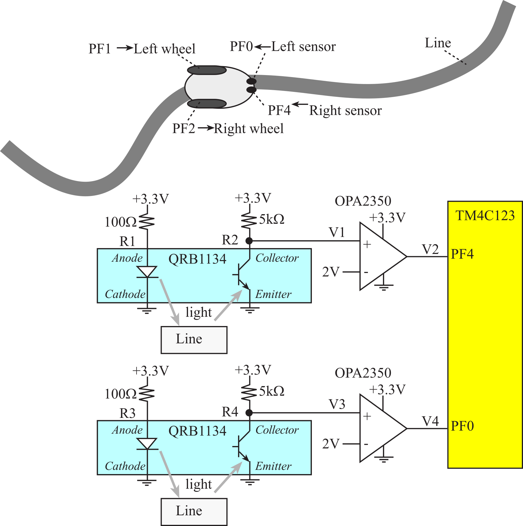
Figure 7.2.1. Robot with two drive wheels and two line-sensors.
Solution: The QRB1134 LED emits light, which may or may reflect of the surface of the robot track. The QRB1134 sensor voltages, V1 V3, will be high if no reflect light is received or low if the sensor sees a reflective surface. The op amps in open loop mode will create a clean digital signal on V2 and V4 (see section 6.4.6.) The DC motor interface will be described in Section 8.3. Binary Actuators.
To facilitate migration to other microcontrollers Program 7.2.1 presents a board support package, defining a low-level set of routines that perform input/output. For more information on configuring SysTick periodic interrupts see Section 1.9. The purpose of a board support package is to hide as much of the I/O details as possible. We implement a BSP when we expect the high-level system will be deployed onto many low-level platforms. The BSP in Program 7.2.1 can be adapted to any microcontroller, any bus speed, and any GPIO pins.
// TM4C123 specific code
#define BUS 80000000
#define PF21 (*((volatile unsigned long *)0x40025018))
#define PF4 (*((volatile unsigned long *)0x40025040))
#define PF0 (*((volatile unsigned long *)0x40025004))
void Robot_Init(void){
DisableInterrupts(); // disable during initialization
PLL_Init(Bus80MHz); // bus clock at 80 MHz
SYSCTL_RCGCGPIO_R |= 0x20; // 1) activate clock for Port F
SysTick_Init(T10ms,2); // initialize SysTick timer
GPIO_PORTF_LOCK_R = 0x4C4F434B; // 2) unlock GPIO Port F
GPIO_PORTF_CR_R = 0x1F; // allow changes to PF4-0
GPIO_PORTF_AMSEL_R = 0x00; // 3) disable analog on PF
GPIO_PORTF_PCTL_R = 0x00000000; // 4) PCTL GPIO on PF4-0
GPIO_PORTF_DIR_R = 0x0E; // 5) PF4,PF0 in, PF3-1 out
GPIO_PORTF_AFSEL_R = 0x00; // 6) disable alt funct on PF7-0
GPIO_PORTF_DEN_R = 0x1F; // 7) enable digital I/O on PF4-0
EnableInterrupts(); // enable after initialization
}
uint32_t Robot_Input(void){
return PF0+(PF4>>3); // read sensors
}
void Robot_Output(uint32_t out){
PF21 = out<<1;
}
void SysTick_Restart(uint32_t time){
NVIC_ST_RELOAD_R = time;
NVIC_ST_CURRENT_R = 0;
}
Program 7.2.1a. Board support package for the robot for TM4C123. Output pins on PF2 and PF1. Line sensor inputs on PF4 and PF0.
// MSPM0G3507 specific code
#define BUS 80000000
void Robot_Init(void){
__disable_irq();
Clock_Init80MHz(0);
LaunchPad_Init();
SysTick_Init(T10ms,2);
IOMUX->SECCFG.PINCM[PB7INDEX] = 0x00040081;
IOMUX->SECCFG.PINCM[PB6INDEX] = 0x00040081;
IOMUX->SECCFG.PINCM[PB1INDEX] = 0x00000081;
IOMUX->SECCFG.PINCM[PB0INDEX] = 0x00000081;
GPIOB->DOE31_0 |= 0x03;
__enable_irq();
}
void Robot_Output(uint32_t data){
GPIOB->DOUT31_0 = (GPIOB->DOUT31_0&(~0x03))|data;
}
uint32_t Robot_Input(void){
return (GPIO_PORTB_DATA_R&0xC0)>>6;
}
void SysTick_Restart(uint32_t time){
SysTick->LOAD = time;
SysTick->VAL = 0;
}
Program 7.2.1b. Board support package for the robot for MSPM0. Output pins on PB1 and PB0. Line sensor inputs on PB7 and PB6.
The first step in designing a FSM is to create some states. The outputs of a Moore FSM are only a function of the current state. A Moore implementation was chosen because we define our states by what believe to be true, and we will have one action (output) that depends on the state. Each state is given a symbolic name where the state name either describes "what we know" or "what we are doing". We could have differentiated between a little off to the left and way off to the left, but this solution creates a simple solution with 3 states. See Figure 7.2.2.
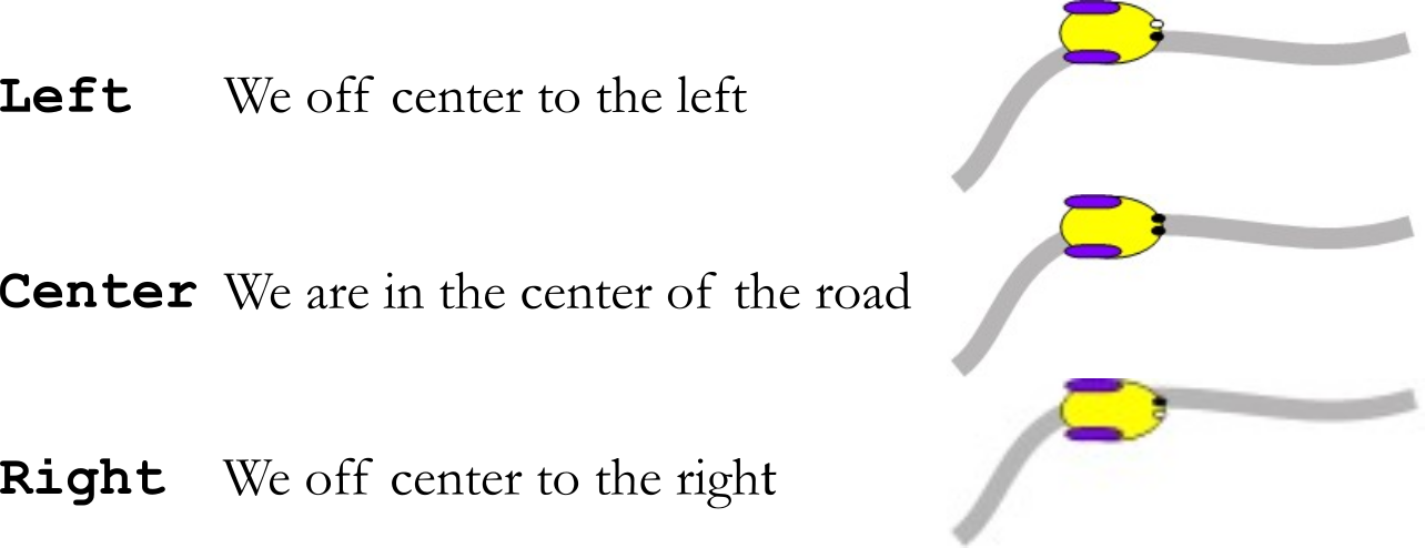
Figure 7.2.2. The sensor inputs for the three states.
The finite state machine implements this line-tracking algorithm. Each state has a 2-bit output value, and four next state pointers. The strategy will be to:
Go straight if we are on the line.
Turn right if we are off to the left.
Turn left if we are off to the right.
Finally, we implement the heuristics by defining the state transitions, as illustrated in Figure 7.2.3 and Table 7.2.1. If we used to be in the left state and completely lose the line (input 00), then we know we are left of the line. Similarly, if we used to be in the right state and completely lose the line (input 00), then we know we are right of the line. However, we used to be on the center of the line and then completely lose the line (input 00), we do not know we are right or left of the line. The machine will guess we went right of the line. In this implementation, we put a constant delay of 10ms in each state. Nevertheless, we put the time to wait into the machine as a parameter for each state to provide for clarity of how it works and simplify possible changes in the future. If we are off to the right (input 01), then it will oscillate between Center and Right states, making a slow turn left. If we are off to the left (input 10), then it will oscillate between Center and Left states, making a slow turn right.
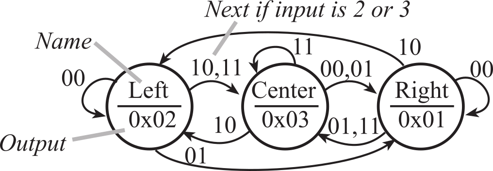
Figure 7.2.3. Graphical form of a Moore FSM that implements a line tracking robot.
|
|
|
|
Input |
|||
|
State |
Motor |
Delay |
00 |
01 |
10 |
11 |
|
Center |
1,1 |
1 |
Right |
Right |
Left |
Center |
|
Left |
1,0 |
1 |
Left |
Right |
Center |
Center |
|
Right |
0,1 |
1 |
Right |
Center |
Left |
Center |
Table 7.2.1. Tabular form of a Moore FSM that implements a line tracking robot.
The first step in designing the software is to decide on the sequence of operations. When running the controller in the main program, we perform output, delay, input, next. The delay step in this approach is inefficient because the software does not do any useful work. If there are no other tasks to perform, it should at least go into low-power sleep mode.
1) Initialize timer and
directions registers
2) Specify initial state
3) Perform FSM controller in the main loop
a) Output to DC
motors, which depends on the state
b) Delay, which
depends on the state
c) Input from line
sensors
d) Change states,
which depends on the state and the input
To allow the main to do other work, we can run the controller in an interrupt service routine. The main program initializes the timer and GPIO pins, and then the main loop can perform other tasks or sleep. The ISR performs input, next, output, delay. The delay step does not actually wait, but rather it configures the periodic timer for when the next interrupt should occur.
c) Input from line sensors
d) Change states,
which depends on the state and the input
a) Output to DC
motors, which depends on the state
b) Delay, which
depends on the state
The second step is to define the FSM graph using a data structure. Program 7.2.2 shows a table implementation of the Moore FSM. This implementation uses a table data structure, where each state is an entry in the table, and state transitions are defined as indices into this table. The four Next parameters define the input-dependent state transitions. The wait times are defined in the software as fixed-point decimal numbers with units of 0.01s. The label Center is more descriptive than the state number 0. Notice the 1-1 correspondence between the tabular form in Table 7.2.1 and the software specification of fsm[3]. This 1-1 correspondence makes it possible to prove the software exactly executes the FSM as described in the table.
struct State{
uint32_t Out; // 2-bit output
uint32_t Delay; // time in bus cycles
uint8_t Next[4];
};
typedef const struct State State_t;
#define Center 0
#define Left 1
#define Right 2
#define T10ms (BUS/100)
State_t fsm[3] = {
{0x03, T10ms, { Right, Right, Left, Center }}, // Center of line
{0x02, T10ms, { Left, Right, Center, Center }}, // Left of line
{0x01, T10ms, { Right, Center, Left, Center }} // Right of line
};
uint32_t S; // index to the current state
void SysTick_Handler(void){
uint32_t input, output; // state I/O
input = Robot_Input(); // read sensors
S = fsm[S].Next[input]; // next depends on input and state
output = fsm[S].Out; // set output from FSM
Robot_Output(output); // do output to two motors
SysTick_Restart(fsm[S].Delay); // set time for next interrupt
}
int main(void){
S = Center; // initial state
Robot_Init(); // Initialize GPIO, SysTick
while(1){
}
}
Program 7.2.2. Table implementation of a Moore FSM.
Program 7.2.3 uses a linked structure, where each state is a node, and state transitions are defined as pointers to other nodes. Again, notice the 1-1 correspondence between Table 7.2.1 and the software specification of fsm[3].
struct State {
uint32_t Out; // 2-bit output
uint32_t Delay; // time in bus cycles
const struct State *Next[4];
};
typedef const struct State State_t;
#define Center &fsm[0]
#define Left &fsm[1]
#define Right &fsm[2]
State_t *pt; // state pointer
State_t fsm[3] = {
{0x03, T10ms, { Right, Right, Left, Center }}, // Center of line
{0x02, T10ms, { Left, Right, Center, Center }}, // Left of line
{0x01, T10ms, { Right, Center, Left, Center }} // Right of line
};
void SysTick_Handler(void){
uint32_t input, output; // state I/O
input = Robot_Input(); // read sensors
pt = pt->Next[input]; // next depends on input and state
output = pt->Out; // set output from FSM
Robot_Output(output); // do output to two motors
SysTick_Restart(fsm[S].Delay); // set time for next interrupt
}
int main(void){
pt = Center; // initial state
Robot_Init(); // Initialize GPIO, SysTick
while(1){
}
}
Program 7.2.3. Pointer implementation of a Moore FSM.
Observation: The table implementation requires less memory space for the FSM data structure, but the pointer implementation will run faster.
To add more output signals, we simply increase the precision of the Out field. To add more input lines, we increase the size of the next field. If there are n input bits, then the size of the next field will be 2n. For example, if there are four input lines, then there are 16 possible combinations, where each input possibility requires a Next value specifying where to go if this combination occurs.
Example 7.2.2. The goal is to design a finite state machine robot controller, as illustrated in Figure 7.2.4. Because the outputs cause the robot to change states, we will use a Mealy implementation. The outputs of a Mealy FSM depend on both the input and the current state. This robot has mood sensors that are interfaced to PB7 and PB6. The robot has four possible conditions:
00 OK, the robot is feeling fine
01 Tired, the robot energy levels are low
10 Curious, the robot senses activity around it
11 Anxious, the robot senses danger
There are four actions this robot can perform, which are triggered by pulsing (make high, then make low) one of the four signals interfaced to Port B.
PB3 SitDown,
assuming it is standing, it will perform moves to sit down
PB2 StandUp,
assuming it is sitting, it will perform moves to stand up
PB1 LieDown,
assuming it is sitting, it will perform moves to lie down
PB0 SitUp, assuming
it is sleeping, it will perform moves to sit up
Solution: For this design we can list heuristics describing how the robot is to operate:
If the robot is OK, it will
stay in its current state.
If the robot's energy levels
are low, it will go to sleep.
If the robot senses activity
around it, it will awaken from sleep.
If the robot senses danger,
it will stand up.
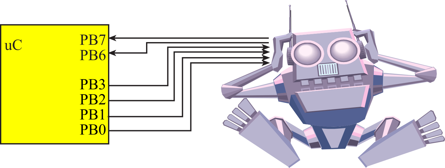
Figure 7.2.4. Robot interface.
These rules are converted into a finite state machine graph, as shown in Figure 7.2.5. Each arrow specifies both an input and an output. For example, the "Tired/SitDown" arrow from Stand to Sit states means if we are in the Stand state and the input is Tired, then we will output the SitDown command and go to the Sit state. Mealy machines can have time delays, but this example just didn't have time delays.
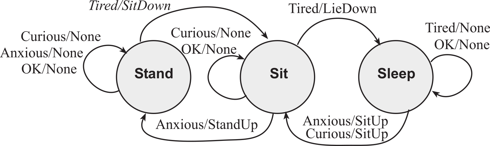
Figure 7.2.5. Mealy FSM for a robot controller.
The first step in designing the software is to decide on the sequence of operations.
1) Initialize directions
registers
2) Specify initial state
3) Perform FSM controller
a) Input from
sensors
b) Output to the
robot, which depends on the state and the input
c) Change states,
which depends on the state and the input
Program 7.2.4 presents the low-level software I/O functions for the robot. Separating low-level code into a board support package makes it easier to port this software to other microcontrollers.
|
// TM4C123 void Robot_Init(void){ volatile uint32_t delay; PLL_Init(Bus80MHz); SYSCTL_RCGCGPIO_R |= 0x02; delay = SYSCTL_RCGCGPIO_R; GPIO_PORTB_PCTL_R &= ~0xFF0000FF; GPIO_PORTB_DIR_R |= 0x03; GPIO_PORTB_DIR_R &= ~0xC0; GPIO_PORTB_AFSEL_R &= ~0xC3; GPIO_PORTB_DR8R_R |= 0x03; GPIO_PORTB_DEN_R |= 0xC3; } void Robot_Output(uint32_t data){ GPIO_PORTB_DATA_R = (GPIO_PORTB_DATA_R&(~0x03))|data; } uint32_t Robot_Input(void){ return (GPIO_PORTB_DATA_R&0xC0)>>6; } |
// MSPM0G3507 void Robot_Init(void){ Clock_Init80MHz(0); LaunchPad_Init(); IOMUX->SECCFG.PINCM[PB7INDEX] = 0x00040081; IOMUX->SECCFG.PINCM[PB6INDEX] = 0x00040081; IOMUX->SECCFG.PINCM[PB1INDEX] = 0x00000081; IOMUX->SECCFG.PINCM[PB0INDEX] = 0x00000081; GPIOB->DOE31_0 |= 0x03; }
void Robot_Output(uint32_t data){ GPIOB->DOUT31_0 = (GPIOB->DOUT31_0&(~0x03))|data; } uint32_t Robot_Input(void){ return (GPIOB->DIN31_0&0xC0)>>6; } |
Program 7.2.4. Low-level software for the robot.
The second step is to define the FSM graph using a linked data structure. Two possible implementations of the Mealy FSM are presented. The implementation in Program 7.2.5 defines the outputs as simple numbers, where each pulse is defined as the bit mask required to cause that action. The four Next parameters define the input-dependent state transitions.
struct State{
uint32_t Out[4]; // outputs
const struct State *Next[4]; // next
};
typedef const struct State State_t;
#define Stand &FSM[0]
#define Sit &FSM[1]
#define Sleep &FSM[2]
#define None 0x00
State_t FSM[3]={
{{None,SitDown,None,None}, //Standing
{Stand,Sit,Stand,Stand}},
{{None,LieDown,None,StandUp},//Sitting
{Sit,Sleep,Sit,Stand }},
{{None,None,SitUp,SitUp}, //Sleeping
{Sleep,Sleep,Sit,Sit}}
};
int main(void){ State_t *pt; // current state
uint32_t input;
Robot_Init(); // clock and GPIO initialization
pt = Stand; // initial state
while(1){
input = Robot_Input(); // input=0-3
Robot_Output(pt->Out[Input]);
// pulse
Robot_Output(None);
pt = pt->Next[Input]; // next state
}
}
Program 7.2.5. Outputs defined as numbers for a Mealy Finite State Machine.
Program 7.2.6 uses functions to affect the output. Although the functions in this solution perform simple output, this implementation could be used when the output operations are complex. Again proper memory allocation is required if we wish to implement a stand-alone or embedded system. The const qualifier is used to place the FSM data structure in flash ROM.
struct State{
void *CmdPt[4]; // outputs are function pointers
const struct State *Next[4]; // next
};
typedef const struct State State_t;
#define Stand &FSM[0]
#define Sit &FSM[1]
#define Sleep &FSM[2]
void doNone(void){};
void doSitDown(void){
Robot_Output(SitDown);
Robot_Output(None); // pulse
}
void doStandUp(void){
Robot_Output(StandUp);
Robot_Output(None); // pulse
}
void doLieDown(void){
Robot_Output(LieDown);
Robot_Output(None); // pulse
}
void doSitUp(void) {
Robot_Output(SitUp);
Robot_Output(None); // pulse
}
State_t FSM[3]={
{{(void*)&doNone,(void*)&doSitDown,(void*)&doNone,(void*)&doNone}, //Standing
{Stand,Sit,Stand,Stand}},
{{(void*)&doNone,(void*)doLieDown,(void*)&doNone,(void*)&doStandUp},//Sitting
{Sit,Sleep,Sit,Stand }},
{{(void*)&doNone,(void*)&doNone,(void*)&doSitUp,(void*)&doSitUp}, //Sleeping
{Sleep,Sleep,Sit,Sit}}
};
int main(void){ State_t *pt; // current state
uint32_t input;
Robot_Init(); // clock and GPIO initialization
pt = Stand; // initial state
while(1){
input = Robot_Input(); // input=0-3
((void(*)(void))pt->CmdPt[Input])(); // function
pt = pt->Next[input]; // next state
}
}
Program 7.2.6. Outputs defined as functions for a Mealy Finite State Machine.
Observation: To make the FSM respond quicker, we could implement a time delay function that returns immediately if an alarm condition occurs. If no alarm exists, it waits for the specified delay. Similarly, we could return from the time delay on a change in input.
: What happens if the robot is sleeping then becomes anxious?
We can expand the syntax of a finite state machine to support sensor integration. A finite state machine uses inputs to affect state changes. These state changes depend on input values being a specific value. However, there are natural ways to combine sensor data to make state changes. Figure 7.2.6 shows an RSLK robot with many sensors.
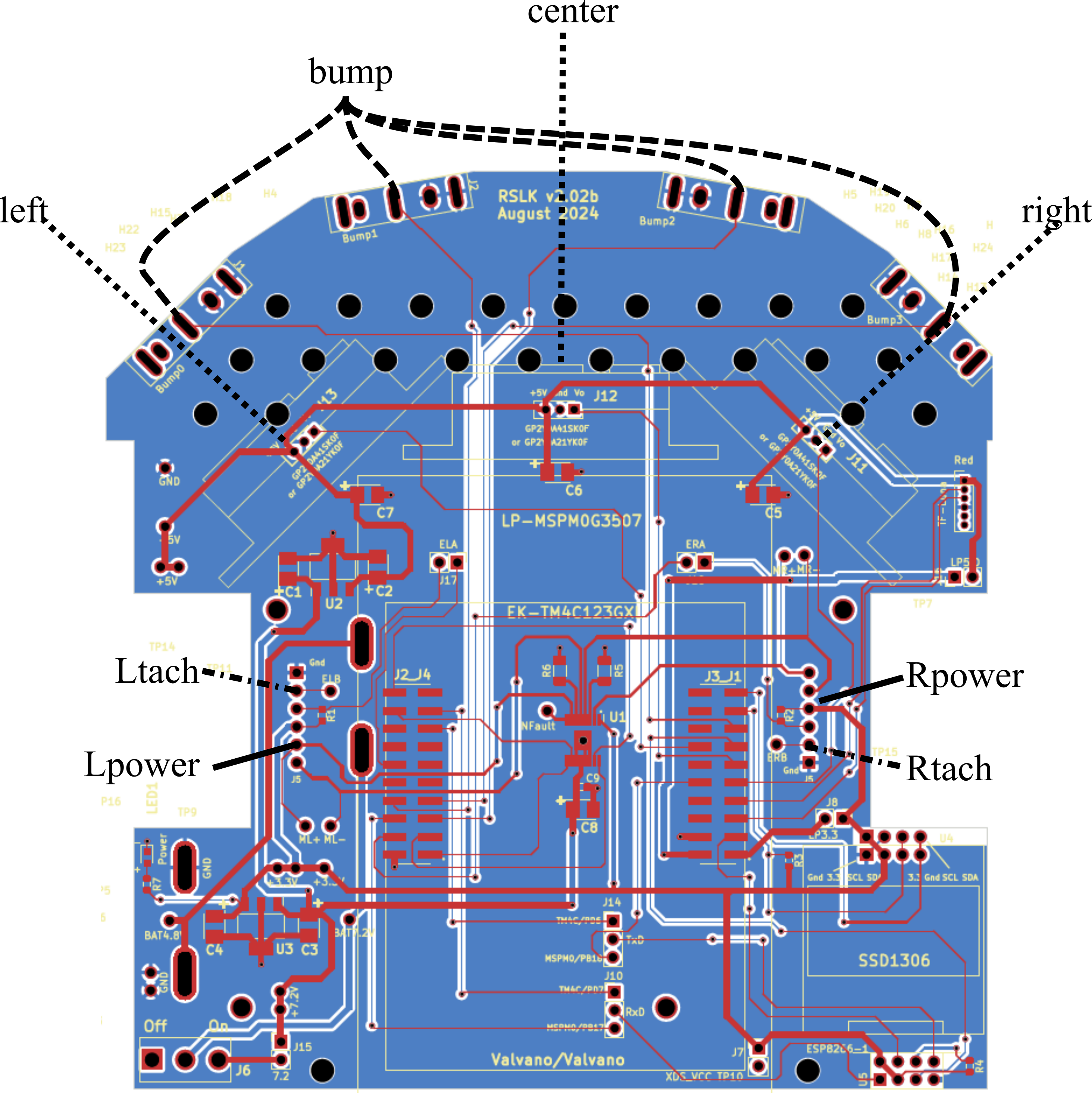
Figure 7.2.6. RSLK Robot with sensors and actuators
Let Ltach be the wheel speed measured by the left tachometer. Let bump be a four bit binary number read from the negative logic switches on the front of the robot. Let left be the distance to the left wall measured by the IR distance sensor. Let right be the distance to the right wall measured by another IR distance sensor. Let center be the distance to closest object in front of the robot measured by the TF Luna time of flight sensor Let Lpower be the actuator duty cycle value being delivered to the left motor. Let Rpower be the actuator duty cycle value being delivered to the right motor. First, consider state changes based on simultaneous sensor readings. Notice in each case the AND, signifying simultaneous condition. For example,
• Go to Collision state if Ltach used to be above 1rps AND bump is not 0x0F
• Go to OffLeft state if left is below 250mm AND center is above 200mm
• Go to Stalled state if Ltach is below 1rps, Lpower is above 1000, AND bump is 0x3F
Next, consider state changes based on alternative sensor readings. Notice in each case the OR, signifying either condition. For example,
• Go to Collision state if center is less than 10 mm OR bump is not 0x3F
• Go to TurnRight state if left is below 200mm OR right is above 300mm
One of the challenging design decisions will be to create a data structure to support this sensor integration. A very flexible approach is to create a set of functions to implement the logic. In the following structure, pOutput is a pointer to a function that performs the output operation based on the state number. pInput is a pointer to a function that performs input. If the input condition is true, it will return a state number to go to. If the input condition is false, it will return -1. The functions are sorted in priority order such that the first input condition to trigger will be executed and the remaining input conditions will be skipped. If none of the input conditions trigger, then the machine will stay in the current state.
struct State{
void (*pOutput)(void);
uint32_t NumInputFunctions;
int32_t (*pInput[10])(void);
};
typedef const struct State State_t;
Example 7.2.3. Redesign a traffic light controller orginally presented in Section 4.4.1 of Volume 1 using this function syntax. Figure 7.2.7 describes the state transition graph of this controller. Program 7.2.7 implements this traffic light controller.
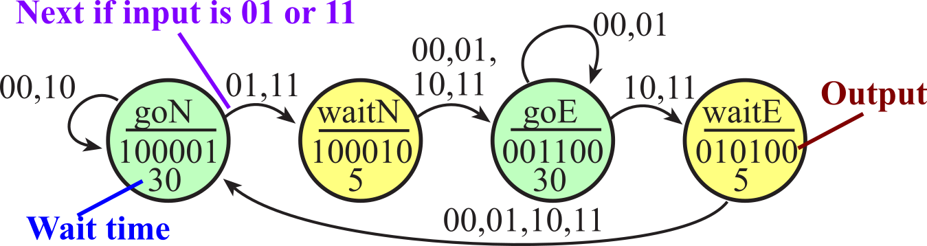
Figure 7.2.7. State transition graph for a simple traffic controller.
#define goN 0
#define waitN 1
#define goE 2
#define waitE 3
void GoNorth(void){
TrafficOutput(0x21); // lights green on north, red on east
SysTick_Wait10ms(3000); // 3 sec
}
void WaitNorth(void){
TrafficOutput(0x22); // lights yellow on north, red on east
SysTick_Wait10ms(500); // 0.5 sec
}
void GoEast(void){
TrafficOutput(0x0C); // lights green on east, red on north
SysTick_Wait10ms(3000); // 3 sec
}
void WaitEast(void){
TrafficOutput(0x22); // lights yellow on east, red on north
SysTick_Wait10ms(500); // 0.5 sec
}
uint32_t CS ; // Current State
int32_t CheckForEast(void){
if(TrafficInput()&1){
return waitN; // there are cars on east
}
return -1; // no cars on east
}
int32_t SwitchToEast(void){
return goE; // there are cars on east
}
int32_t CheckForNorth(void){
if(TrafficInput()&2){
return waitE; // there are cars on north
}
return -1; // no cars on north
}
int32_t SwitchToNorth(void){
return goN; // there are cars on north
}
State_t FSM[4]={
{&GoNorth, 1,{&CheckForEast}},
{&WaitNorth,1,{&SwitchToEast}},
{&GoEast, 1,{&CheckForNorth}},
{&WaitEast, 1,{&SwitchToNorth}}
};
int main(void){ int32_t next;
Clock_Init80MHz(0);
SysTick_Init();
Traffic_Init();
CS = goN;
while(1){
(*(FSM[CS].pOutput))(); // perform output
for(int i=0; i<FSM[CS].NumInputFunctions;i++){
next = (*(FSM[CS].pInput[i]))(); // Check input
if(next >= 0){
CS = next;
break;
}
}
}
}
Program 7.2.7. Table implementation of a Moore FSM using function pointers.
Observation
The simple solutions presented in Section 4.4.1 of Volume 1 are much better code for this simple problem.
This very complex solution to this very simple problem is includes to describe the process
of implementing sensor fusion using the FSM structure.
7.2.2. Petri Nets
In the last section, we presented finite state machines as a formal mechanism to describe systems with inputs and outputs. In this section, we present two methods to describe synchronization in complex systems: Petri Nets and Kahn Process Networks. Petri Nets can be used to study the dynamic concurrent behavior of network-based systems where there is discrete flow, such as packets of data. A Petri Net is comprised of Places, Transition, and Arcs. Places, drawn as circles in Figure 7.2.8, can contain zero, one, or more tokens. Consider places as variables (or buffers) and tokens as discrete packets of data. Tokens are drawn in the net as dots with each dot representing one token. Formally, the tokens need not comprise data and could simply represent the existence of an event. Transitions, drawn as vertical bars, represent synchronizing actions. Consider transitions as software that performs work for the system. From a formal perspective, a Petri Net does not model time delay. But, from a practical viewpoint we know executing software must consume time. The arcs, drawn as arrows, connect places to transitions. An arc from a place to a transition is an input to the transition, and an arc from a transition to a place is an output of the transition.
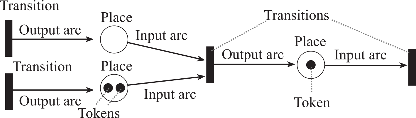
Figure 7.2.8. Petri Nets are built with places, transitions and arcs. Places can hold tokens.
For example, an input switch could be modeled as a device that inserts tokens into a place. The number of tokens would then represent the number of times the switch has been pressed. An alphanumeric keyboard could also be modeled as an input device that inserts tokens into a place. However, we might wish to assign an ASCII string to the token generated by a keyboard device. An output device in a Petri Net could be modeled as a transition with only input arcs but no output arcs. An output device consumes tokens (data) from the net.
Arcs are never drawn from place to place, nor from transition to transition. Transition node is ready to fire if and only if there is at least one token at each of its input places. Conversely, a transition will not fire if one or more input places is empty. Firing a transition produces software action (a task is performed). Formally, firing a transition will consume one token from each of its input places and generate one token for each of its output places. Figure 7.2.9 illustrates an example firing. In this case, the transition will wait for there to be at least one token in both its input places. When it fires it will consume two tokens and merge them into one token added to its output place. In general, once a transition is ready to fire, there is no guarantee when it will fire. One useful extension of the Petri Net assigns a minimum and maximum time delay from input to output for each transition that is ready to fire.
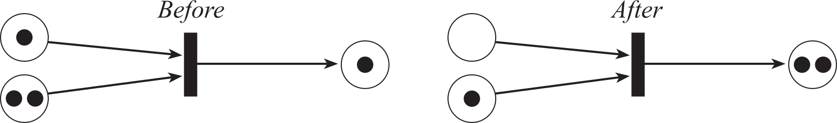
Figure 7.2.9. Firing a transition consumes one token at each input and produces one token at each output.
Figure 7.2.10 illustrates a sequential operation. The three transitions will fire in a strictly ordered sequence: first t1, next t2, and then t3.
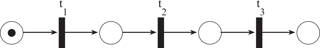
Figure 7.2.10. A Petri Net used to describe a sequential operation.
Figure 7.2.11 illustrates concurrent operation. Once transition t1 fires, transitions t2 and t3 are running at the same time. On a distributed system t2 and t3 may be running in parallel on separate computers. On a system with one processor, two operations are said to be running concurrently if they are both ready to run. Because there is a single processor, the tasks must run one at a time.
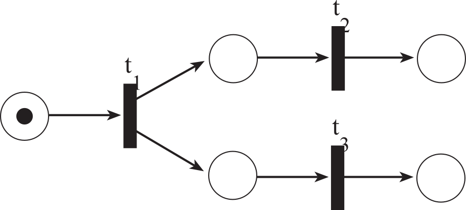
Figure 7.2.11. A Petri Net used to describe concurrent operations.
Figure 7.2.12 demonstrates a conflict or race condition. Both t1 and t2 are ready to fire, but the firing of one leads to the disabling of the other. It would be a mistake to fire them both. A good solution would be to take turns in some fair manner (flip a coin or alternate). A deterministic model will always produce the same output from a given starting condition or initial state. Because of the uncertainty when or if a transition will fire, a system described with a Petri Net is not deterministic.
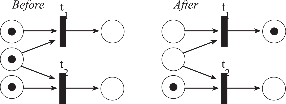
Figure 7.2.12. If t1 were to fire, it would disable t2. If t2 were to fire, it would disable t1.
Figure 7.2.13 describes an assembly line on a manufacturing plant. There are two robots. The first robot picks up one Part1 and one Part2, placing the parts together. After the robot places the two parts, it drills a hole through the combination, and then places the partial assembly into the Partial bin. The second robot first combines Part3 with the partial assembly and screws them together. The finished product is placed into the Done bin. The tokens represent the state of the system, and transitions are actions that cause the state to change.
The three supply transitions are input machines that place parts into their respective parts bins. The tokens in places Part1, Part2, Part3, Partial, and Done represent the number of components in their respective bins. The first robot performs two operations but can only perform one at a time. The Rdy-to-P&P place has a token if the first robot is idle and ready to pick and place. The Rdy-to-drill place has a token if the first robot is holding two parts and is ready to drill. The Pick&Place transition is the action caused by the first robot as it picks up two parts placing them together. The Drill transition is the action caused by the first robot as it drills a hole and places the partial assembly into the Partial bin.
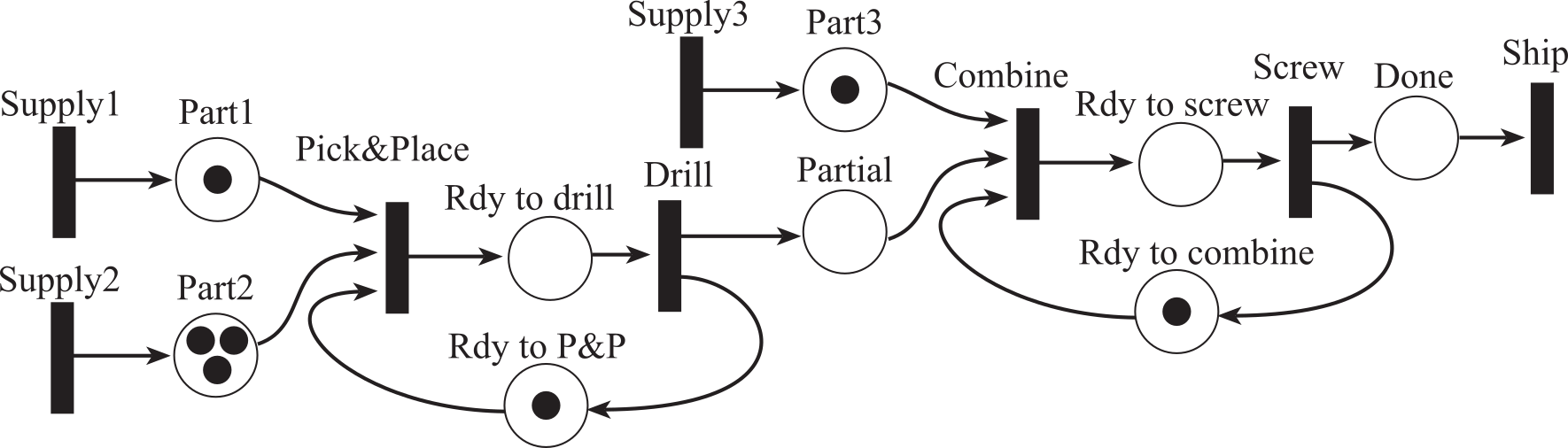
Figure 7.2.13. A Petri Net used to describe an assembly line.
The first robot performs two operations but can only perform one at a time. The Rdy-to-P&P place has a token if the first robot is idle and ready to pick and place. The Rdy-to-drill place has a token if the first robot is holding two parts and is ready to drill. The Pick&Place transition is the action caused by the first robot as it picks up two parts placing them together. The Drill transition is the action caused by the first robot as it drills a hole and places the partial assembly into the Partial bin.
The second robot performs two operations. The Rdy-to-combine place has a token if the second robot is idle and ready to combine. The Rdy-to-screw place has a token if the second robot is holding two parts and is ready to screw. The Combine transition is the action caused by the second robot as it picks up a Part3 and a Partial combining them together. The Screw transition is the action caused by the second robot as it screws it together and places the completed assembly into the Done bin. The Ship transition is an output machine that sends completed assemblies to their proper destination.
: Assuming no additional input machines are fired, run the Petri Net shown in Figure 7.2.13 until it stalls. How many competed assemblies are shipped?
7.2.3. Kahn Process Networks
Gilles Kahn first introduced the Kahn Process Network (KPN). We use KPNs to model distributed systems as well as signal processing systems. Each node represents a computation block communicating with other nodes through unbounded FIFO channels. The circles in Figure 7.2.14 are computational blocks and the arrows are FIFO queues. The resulting process network exhibits deterministic behavior that does not depend on the various computation or communication delays. As such, KPNs have found many applications in modeling embedded systems, high-performance computing systems, and computational tasks.
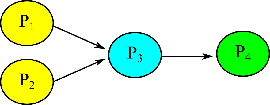
Figure 7.2.14. A Kahn Process Network consists of process nodes linked by unbounded FIFO queues.
For each FIFO, only one process puts, and only one process gets. Figure 7.2.14 shows a KPN with four processes and three edges (communication channels). Processes P1 and P2 are producers, generating data into channels A and B respectively. Process P3 consumes one token from channel A and another from channel B (in either order), and then Process P3 produces one token into channel C. Process P4 is a consumer because it consumes tokens.
We can use a KPN to describe signal processing systems where infinite streams of data are transformed by processes executing in sequence or parallel. Streaming data means we input/analyze/output one data packet at a time without the desire to see the entire collection of data all at once. Despite parallel processes, multitasking or parallelism are not required for executing this model. In a KPN, processes communicate via unbounded FIFO channels. Processes read and write atomic data elements, or alternatively called tokens, from and to channels. The read token is equivalent to a FIFO get and the write token is a FIFO put. In a KPN, writing to a channel is non-blocking. This means we expect the put FIFO command to always succeed. In other words, the FIFO never becomes full. From a practical perspective, we can use KPN modeling for situations where the FIFOs never actually do become full. Furthermore, the approximate behavior of a system can still be deemed for systems where FIFO full errors are infrequent. For these approximations we could discard data with the FIFO becomes full on a put instead of waiting for there to be free space in the FIFO.
On the other hand, reading from a channel requires blocking. A process that reads from an empty channel will stall and can only continue when the channel contains sufficient data items (tokens). Processes are not allowed to test an input channel for existence of tokens without consuming them. Given a specific input (token) history for a process, the process must be deterministic so that it always produces the same outputs (tokens). Timing or execution order of processes must not affect the result and therefore testing input channels for tokens is forbidden.
To optimize execution some KPNs do allow testing input channels for emptiness as long as it does not affect outputs. It can be beneficial and/or possible to do something in advance rather than wait for a channel. In the example shown in Figure 7.2.14, process P3 must get from both channel A and channel B. The left side of Program 7.2.8 shows the process stalls if the AFifo is empty (even if there is data in the BFifo). If the first FIFO is empty, it might be efficient to see if there is data in the other FIFO to save time (right side of Program 7.2.8).
|
void Process3(void){ int32_t inA, inB, out; while(1){ while(AFifo_Get(&inA)){}; while(BFifo_Get(&inB)){}; out = compute(inA,inB); CFifo_Put(out); } }
|
void Process3(void){ int32_t inA, inB, out; while(1){ if(AFifo_Size()==0){ while(BFifo_Get(&inB)){}; while(AFifo_Get(&inA)){}; } else{ while(AFifo_Get(&inA)){}; while(BFifo_Get(&inB)){}; } out = compute(inA,inB); CFifo_Put(out); } } |
Program 7.2.8. Two C implementations of a process on a KPN. The one on the right is optimized.
Processes of a KPN are deterministic. For the same input history, they must always produce the same output. Processes can be modeled as sequential programs that do reads and writes to ports in any order or quantity if the determinism property is preserved.
KPN processes are monotonic, which means that they only need partial information of the input stream to produce partial information of the output stream. Monotonicity allows parallelism. In a KPN there is a total order of events inside a signal. However, there is no order relation between events in different signals. Thus, KPNs are only partially ordered, which classifies them as an untimed model.
7.3. Design for Manufacturability
Using standard values for resistors and capacitors makes finding parts quicker. Standard values for 1% resistors range from 10 Ω to 2.2 MΩ. We can multiply a number in Tables 7.3.1, 7.3.2, 7.3.3, and 7.3.4 by powers of 10 to select a standard value resistor. For example, if we need a 5 kΩ 1% resistor, the closest number is 49.9*100, or 4.99 kΩ.
Sometimes we need a pair of resistors with a specific ratio. There are 19 pairs of resistors with a 2 to 1 ratio (e.g., 20/10). There is only one pair with a 3 to 1 ratio, 102/34. Similarly, there is only one pair with a 4 to 1 ratio, 102/25.5. There are 19 pairs of resistors with a 5 to 1 ratio (e.g., 100/20). There are 5 pairs of resistors with a 7 to 1 ratio (e.g., 93.1/13.3, 105/15, 140/20, 147/21, 196/28). There are no pairs with ratios of 6, 8, or 9.
Using standard values can greatly reduce manufacturing costs because parts are less expensive, and parts for one project can be used in other projects. Ceramic capacitors can be readily purchased as E6, E12, or E24 standards. Filters scale over a fairly wide range. If a resistor is increased by a factor of x and the capacitor is reduced by a factor of x, the filter response will remain unchanged. For example, the response of a filter that uses 100 kΩ and 0.1 µF will be the same as a filter with 20 kΩ and 0.5 µF. Resistors that are too low will increase power consumption in the circuit, and resistor values that are too high will increase noise. 1% resistors below 100 Ω and above 10 MΩ are hard to obtain. Precision capacitors below 10 pF and above 1 µF are hard to obtain. High-speed applications use lower values of resistors in the 100 Ω to 1 kΩ range, precision equipment operates best with resistors in the 100 kΩ to 1 MΩ range, while portable equipment uses higher values in the 100 kΩ to 10 MΩ range.
E12 standard values for 10% resistors range from 10 Ω to 22 MΩ. We can multiply a number in Table 7.3.1 by powers of 10 to select a standard value 10% resistor or capacitor. The E6 series is every other value and typically available in 20% tolerances.
|
10 |
12 |
15 |
18 |
22 |
27 |
33 |
39 |
47 |
56 |
68 |
82 |
Table 7.3.1. E12 Standard resistor and capacitor values for 10% tolerance.
E24 standard values for 5% resistors range from 10 Ω to 22 MΩ. We can multiply a number in Table 7.3.2 by powers of 10 to select a standard value 5% resistor. For example, if we need a 25 kΩ 5% resistor, the closest number is 24*1000, or 24 kΩ. Capacitors range from 10 pF to 10 µF, although ceramic capacitors above 1 µF can be quite large. The physical dimensions of a capacitor also depend on the rated voltage. You can also get 1% resistors and 1% capacitors in the E24 series. For example, if you need a 0.05 µF capacitor, you can choose an 0.047µF E12, or a 0.051µF E24 capacitor.
|
10 |
11 |
12 |
13 |
15 |
16 |
18 |
20 |
22 |
24 |
27 |
30 |
|
33 |
36 |
39 |
43 |
47 |
51 |
56 |
62 |
68 |
75 |
82 |
91 |
Table 7.3.2. E24 Standard resistor and capacitor values for 5% tolerance.
Table 7.3.3 shows the E96 standard resistance values for 1 % resistors. Table 7.3.4 shows E192 standard resistance values for 0.5, 0.25, 0.1% tolerances. Tables 7.3.1 and 7.3.2 refer to both resistors and capacitors, but the E96 and E192 standards refer only to resistors.
|
10.0 |
10.2 |
10.5 |
10.7 |
11.0 |
11.3 |
11.5 |
11.8 |
12.1 |
12.4 |
12.7 |
13.0 |
|
13.3 |
13.7 |
14.0 |
14.3 |
14.7 |
15.0 |
15.4 |
15.8 |
16.2 |
16.5 |
16.9 |
17.4 |
|
17.8 |
18.2 |
18.7 |
19.1 |
19.6 |
20.0 |
20.5 |
21.0 |
21.5 |
22.1 |
22.6 |
23.2 |
|
23.7 |
24.3 |
24.9 |
25.5 |
26.1 |
26.7 |
27.4 |
28.0 |
28.7 |
29.4 |
30.1 |
30.9 |
|
31.6 |
32.4 |
33.2 |
34.0 |
34.8 |
35.7 |
36.5 |
37.4 |
38.3 |
39.2 |
40.2 |
41.2 |
|
42.2 |
43.2 |
44.2 |
45.3 |
46.4 |
47.5 |
48.7 |
49.9 |
51.1 |
52.3 |
53.6 |
54.9 |
|
56.2 |
57.6 |
59.0 |
60.4 |
61.9 |
63.4 |
64.9 |
66.5 |
68.1 |
69.8 |
71.5 |
73.2 |
|
75.0 |
76.8 |
78.7 |
80.6 |
82.5 |
84.5 |
86.6 |
88.7 |
90.9 |
93.1 |
95.3 |
97.6 |
Table 7.3.3. E96 Standard resistor values for 1% tolerance(resistors only, not for capacitors).
: Let R = 100 kΩ. Find an E24 capacitor such that 1/(2πRC) is as close to 1000 Hz as possible.
: Rather than using an E96 resistor, find two E24 resistors such that the series combination is as close to 127 kΩ as possible.
|
10.0 |
10.1 |
10.2 |
10.4 |
10.5 |
10.6 |
10.7 |
10.9 |
11.0 |
11.1 |
11.3 |
11.4 |
|
11.5 |
11.7 |
11.8 |
12.0 |
12.1 |
12.3 |
12.4 |
12.6 |
12.7 |
12.9 |
13.0 |
13.2 |
|
13.3 |
13.5 |
13.7 |
13.8 |
14.0 |
14.2 |
14.3 |
14.5 |
14.7 |
14.9 |
15.0 |
15.2 |
|
15.4 |
15.6 |
15.8 |
16.0 |
16.2 |
16.4 |
16.5 |
16.7 |
16.9 |
17.2 |
17.4 |
17.6 |
|
17.8 |
18.0 |
18.2 |
18.4 |
18.7 |
18.9 |
19.1 |
19.3 |
19.6 |
19.8 |
20.0 |
20.3 |
|
20.5 |
20.8 |
21.0 |
21.3 |
21.5 |
21.8 |
22.1 |
22.3 |
22.6 |
22.9 |
23.2 |
23.4 |
|
23.7 |
24.0 |
24.3 |
24.6 |
24.9 |
25.2 |
25.5 |
25.8 |
26.1 |
26.4 |
26.7 |
27.1 |
|
27.4 |
27.7 |
28.0 |
28.4 |
28.7 |
29.1 |
29.4 |
29.8 |
30.1 |
30.5 |
30.9 |
31.2 |
|
31.6 |
32.0 |
32.4 |
32.8 |
33.2 |
33.6 |
34.0 |
34.4 |
34.8 |
35.2 |
35.7 |
36.1 |
|
36.5 |
37.0 |
37.4 |
37.9 |
38.3 |
38.8 |
39.2 |
39.7 |
40.2 |
40.7 |
41.2 |
41.7 |
|
42.2 |
42.7 |
43.2 |
43.7 |
44.2 |
44.8 |
45.3 |
45.9 |
46.4 |
47.0 |
47.5 |
48.1 |
|
48.7 |
49.3 |
49.9 |
50.5 |
51.1 |
51.7 |
52.3 |
53.0 |
53.6 |
54.2 |
54.9 |
55.6 |
|
56.2 |
56.9 |
57.6 |
58.3 |
59.0 |
59.7 |
60.4 |
61.2 |
61.9 |
62.6 |
63.4 |
64.2 |
|
64.9 |
65.7 |
66.5 |
67.3 |
68.1 |
69.0 |
69.8 |
70.6 |
71.5 |
72.3 |
73.2 |
74.1 |
|
75.0 |
75.9 |
76.8 |
77.7 |
78.7 |
79.6 |
80.6 |
81.6 |
82.5 |
83.5 |
84.5 |
85.6 |
|
86.6 |
87.6 |
88.7 |
89.8 |
90.9 |
92.0 |
93.1 |
94.2 |
95.3 |
96.5 |
97.6 |
98.8 |
Table 7.3.4. E192 Standard resistor values for tolerances better than 1% (resistors only, not for capacitors).
7.4. Low-Power Design
To save energy, our parents taught us to "turn off the light when you leave the room." We can use this same approach to conserve energy in our embedded system. There are many ways to place analog circuits in low power mode. Some analog circuits have a low-power mode that the software can select. For example, the MAX5353 12-bit DAC requires 280 µA for normal operation, but the software can place it into shut-down mode, reducing the supply current to 2 µA. Some analog circuits have a digital input that the microcontroller can control placing the circuit in active or low-power mode. For example, the TPA731 audio amplifier has a CD pin, see Figure 7.4.1. When this pin is low, the amplifier operates normally with a supply current of 3 mA. However, when CD pin is above 2 V, the supply current drops down to 65 µA. So, when the software wishes to output sound, it sends a command to the MAX5353 to turn on and makes PB0 equal to 0. Conversely, when the software wishes to save power, it sends a shutdown command to the MAX5353 and makes PB0 high.
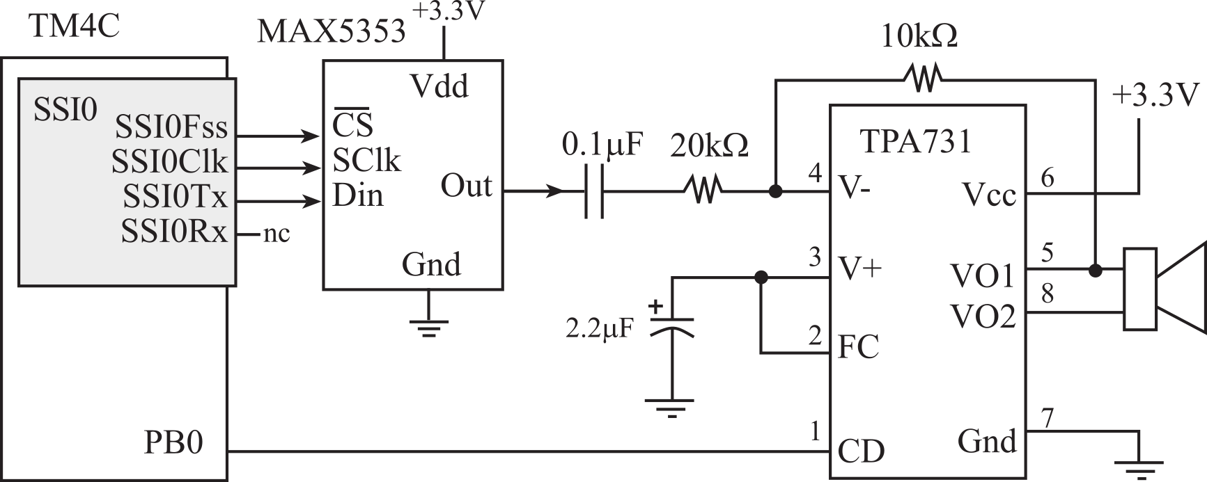
Figure 7.4.1. Audio amplifier that can be placed into low-power mode.
The most effective way to place analog circuit in a low-power state is to shut off its power. Some regulators have a digital signal the microcontroller can control to apply or remove power to the analog circuit. For example, when the OFF pin of the MAX604 regulator is high, the voltage output is regulated to +3.3 V, as shown in Figure 7.4.2. Conversely, when the OFF pin is low, the regulator goes into shut-down mode, and no current is supplied to the analog circuit. When the software wishes to turn off power to the analog circuit, it makes PB0 equal to 0. Conversely, when the software wishes enable the analog circuit, it makes PB0 high. The microcontroller itself always will be powered. However, most microcontrollers can put themselves into a low-power state.
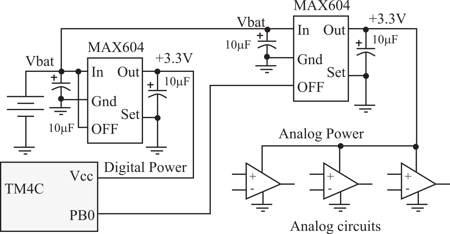
Figure 7.4.2. Power to analog circuits can be controlled by switching on/off the regulator.
We can save power by designing with low-power components. Many analog circuits require a small amount of current, even when active. The MAX494 requires only 200 µA per amplifier. If there are ten op amps in the circuit, the total supply current will be 2 mA. For currents less than 8 mA, we can use the output port itself to power the analog circuit, as shown in Figure 7.4.3. To activate the analog circuit, the microcontroller makes the PB0 high. To turn the power to the analog circuit off, the microcontroller makes PB0 low.
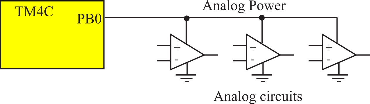
Figure 7.4.3. Power to analog circuits can be delivered from a port output pin.
Considerable power can be saved by reducing the supply voltage. A microcontroller operating at 3.3 V requires less than half the power for an equivalent +5 V system. Power can be saved by turning off modules (like the timer, ADC, UART, and SSI) when not in use. Whenever possible, slowing down the bus clock with the PLL will save power. Many microcontrollers can put themselves into a low-power sleep mode to be awakened by a timer or external event.
: Why is running at 3.3V half the power of running at 5V?
There are many factors that affect the supply current to a microcontroller. The first important factor is bus frequency, as power increases linearly with bus frequency. A second important factor is activating sleep mode when there are no software tasks to perform. The TM4C has a sleep mode, a deep sleep mode, and a hibernate mode. Hibernate mode on the TM4C123 requires 5 µA. The MSPM0G3507 has many low power modes.
SLEEP: 458 µA at 4 MHz
STOP: 47 µA at 32 kHz
STANDBY: 1.5 µA with RTC and SRAM retention
SHUTDOWN: 78 nA with I/O wakeup capability
Hypothesis: Microcontroller power is linearly related to bus frequency.
Assumptions: Supply voltage (Vdd) is constant, independent of frequency. Almost no current flows into or out of the gate. Even though the input resistance is huge, there is a non-neglible effective capacitance, Ceff, which each output must drive.
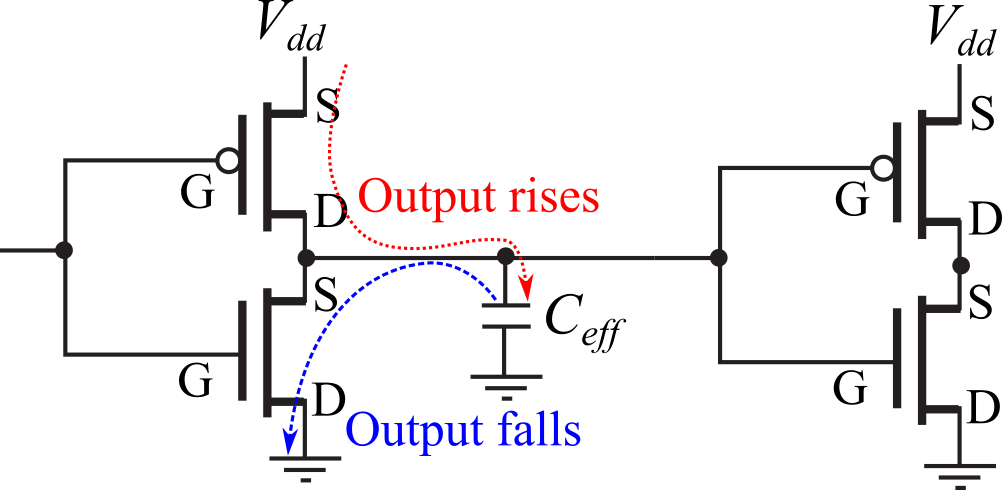
Figure 7.4.4. Digital logic is made with P-channel and N-channel MOSFETs.
Proof: CMOS logic uses a totem pole configuration of P-channel on top of N-channel, see Figure 7.4.4. Since the gate currents are neglected, the current flow from Vdd to ground is determined by the drain-source currents. When the logic level is constant, one transistor is on, and the other is off. So, almost no current flows from Vdd to ground. When the output is low, there is no charge on Ceff. However, when the output changes from low to high, charge is loaded onto Ceff. Current flows from Vdd source to drain through the P channel MOSFET to charge Ceff. The energy stored in the capacitor is U=½Ceff*Vdd2. Unfortunately, when the output changes from high to low, Ceff is discharged, current flowing from drain to source across the N-channel MOSFET. The total energy lost is linearly related to the total number of transitions in the digital circuit. Therefore, the average power is linearly related to the bus frequency
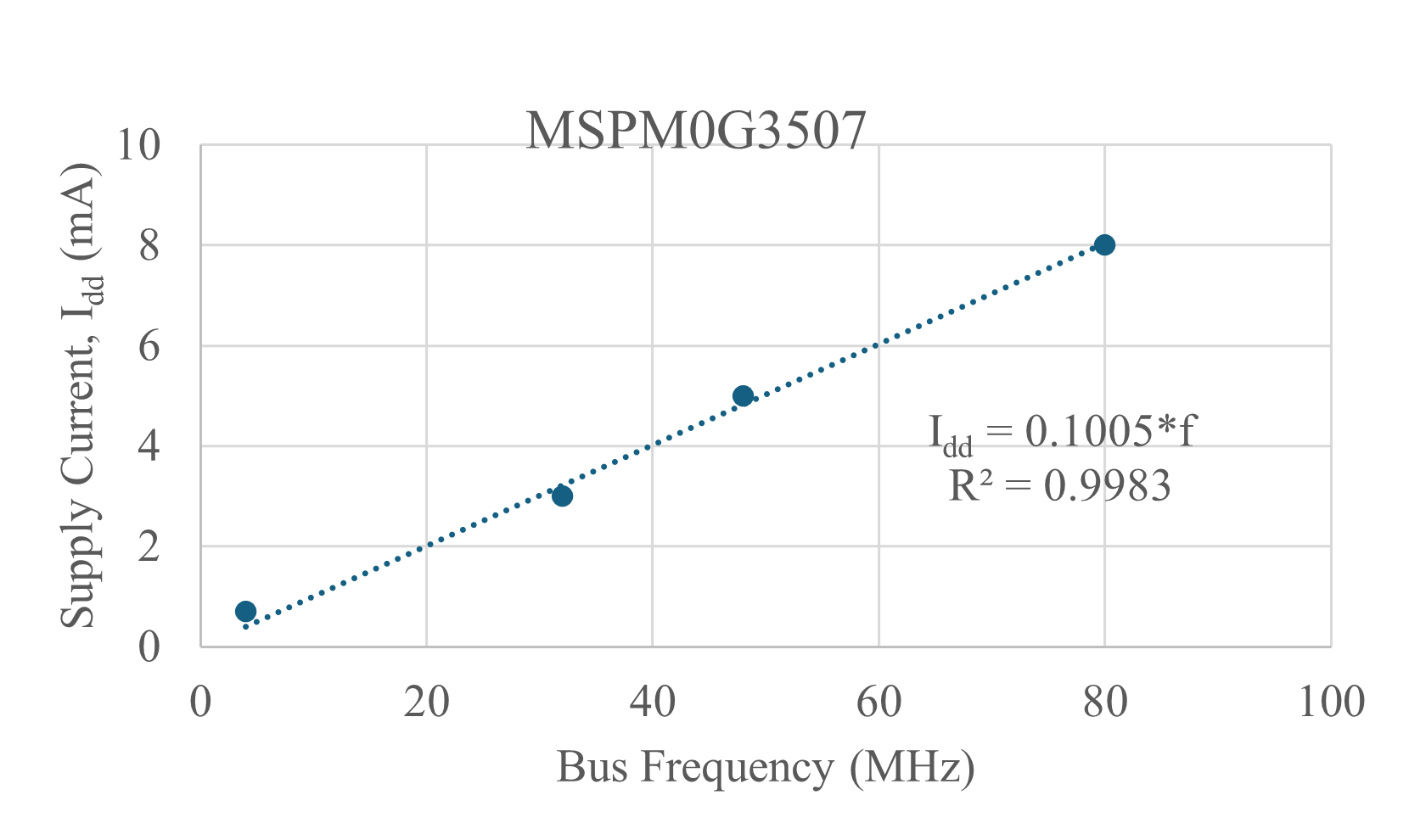
Figure 7.4.5. Supply current versus bus frequency for an MSPM0G3507.