Chapter 1. Introduction
Table of Contents:
- 1.1.
Introduction to Computers
- 1.1.1. von Neumann architecture
- 1.1.2. Harvard architecture
- 1.1.3. Microcontrollers
- 1.1.4. Types of Input/Output
- 1.2. Cortex M Architecture
- 1.2.1. Busses
- 1.2.2. Registers
- 1.2.3. Memory and Bit banding
- 1.2.4. Stack
- 1.2.5. Operating modes
- 1.2.6. Reset
- 1.3.
Embedded Systems
- 1.3.1. Definition and Characteristics
- 1.3.2. Abstraction
- 1.3.3. Interfaces
- 1.3.4. Examples
- 1.3.5. Internet of Things
- 1.4. The Design Process
- 1.4.1. Requirements document
- 1.4.2. Top-down design
- 1.4.3. Flowcharts
- 1.4.4. Parallel, distributed, and concurrent programming
- 1.4.5. Creative discovery using bottom-up design
- 1.5.
Fixed and Floating Point Numbers
- 1.6.
Introduction to Input/Output
- 1.6.1. General Purpose Input/Output (GPIO)
- 1.6.2. TM4C123 pins
- 1.6.3. EK-TM4C123GXL LaunchPad
- 1.6.4. MSPM0G3507 pins
- 1.6.5. LP-MSPM0G3507 LaunchPad
- 1.7.
Digital Logic
- 1.8.
Switch and LED Interfaces
- 1.9.
SysTick Periodic Interrupts
- 1.10.
Ethics
- 1.11.
Introduction to Debugging
- 1.11.1. Debugging Tools
- 1.11.2. Debugging Theory
- 1.11.3. Functional Debugging
- 1.11.4. Performance Debugging
- 1.11.5. Profiling
- 1.12.
Lab 1
The overall objective of this book is to teach the design
of embedded systems. It is effective to learn new techniques by doing them. But
the dilemma in teaching a laboratory-based topic like embedded systems is that
there is a tremendous volume of details that first must be mastered before
hardware and software systems can be designed. The approach taken in this book
is to learn by doing, starting with very simple problems and building up to
more complex systems later in the book.
In this chapter we begin by introducing some terminology and basic components of a computer system. To understand the context of our designs, we will overview the general characteristics of embedded systems. It is in these discussions that we develop a feel for the range of possible embedded applications. Next, we will present a template to guide us in design. We begin a project with a requirements document. Embedded systems interact with physical devices. Often, we can describe the physical world with mathematical models. If a model is available, we can then use it to predict how the embedded system will interface with the real world. When we write software, we mistakenly think of it as one dimensional, because the code looks sequential on the computer screen. Data flow graphs, call graphs, and flow charts are multidimensional graphical tools to understand complex behaviors. Because courses taught using this book typically have a lab component, we will review some practical aspects of digital logic and interfacing signals to the microcontroller.
Next, we show multiple ways to represent data in the computer. Choosing the correct format for data is necessary to implement efficient and correct solutions. Fixed-point numbers are the typical way embedded systems represent non-integer values. Floating-point numbers, typically used to represent non-integer values on a general-purpose computer, will also be presented.
Because embedded systems can be employed in safety critical applications, it is important for engineers be both effective and ethical. Throughout the book we will present ways to verify the system is operating within specifications.
1.1. Introduction to Computers
1.1.1. von Neumann architecture
A computer combines a processor, random access memory (RAM), read only memory (ROM), and input/output (I/O) ports. A bus is defined as a collection of signals, which are grouped for a common purpose. The bus has three types of signals: address, data, and control. Together, the bus directs the data transfer between the various modules in the computer. The common bus in Figure 1.1.1 defines the von Neumann architecture, where instructions are fetched from ROM on the same bus as data fetched from RAM. Software is an ordered sequence of very specific instructions that are stored in memory, defining exactly what and when certain tasks are to be performed. The processor executes the software by retrieving and interpreting these instructions one at a time. A microprocessor is a small processor, where small refers to size (i.e., it fits in your hand) and not computational ability. For example, Intel Xeon, AMD FX and Sun SPARC are microprocessors. A microcomputer is a small computer, where again small refers to size (i.e., you can carry it) and not computational ability. For example, a desktop PC is a microcomputer. ARM Cortex M0+ processors deploy a von Neumann architecture.
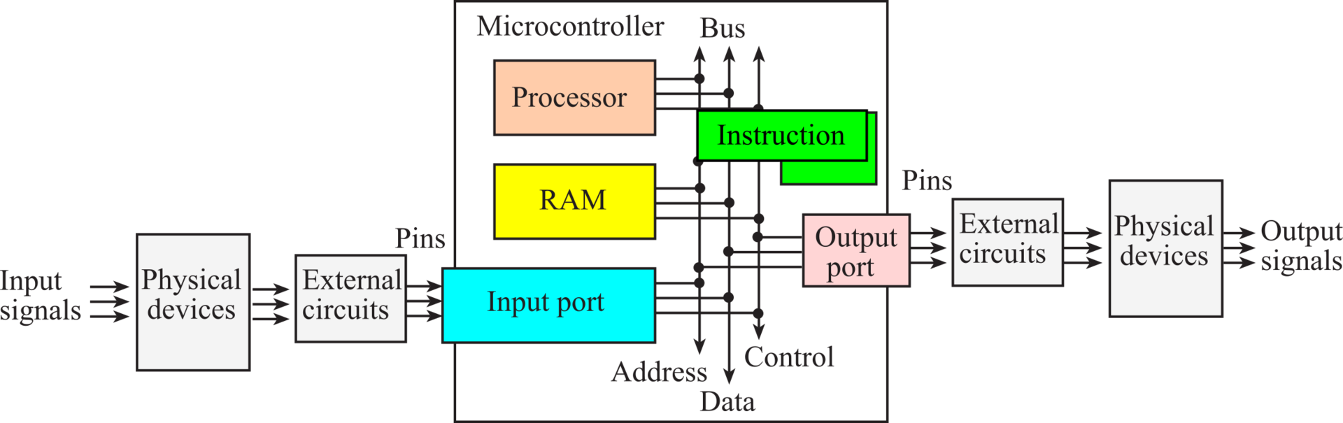
Figure 1.1.1. The basic components of a von Neumann computer including processor, memory and I/O connected with by a single bus.
1.1.2. Harvard architecture
There are five buses on ARM Cortex-M4 processor, as illustrated in Figure 1.1.2. The address specifies which module is being accessed, and the data contains the information being transferred. The control signals specify the direction of transfer, the size of the data, and timing information. The ICode bus is used to fetch instructions from flash ROM. All ICode bus fetches contain 32 bits of data, which may be one or two instructions. The DCode bus can fetch data or debug information from flash ROM. The system bus can read/write data from RAM or I/O ports. The private peripheral bus (PPB) can access some of the common peripherals like the interrupt controller. The multiple-bus architecture allows simultaneous bus activity, greatly improving performance over single-bus architectures. For example, the processor can simultaneously fetch an instruction out of flash ROM using the ICode bus while it writes data into RAM using the system bus. From a software development perspective, the fact that there are multiple buses is transparent. This means we write code like we would on any computer, and the parallel operations occur automatically.
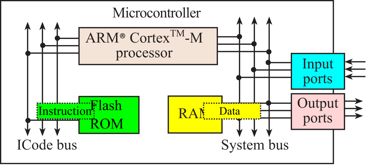
Figure 1.1.2. Harvard architecture of an ARM Cortex-M4. The three signals on each bus are address, data, control. If all these components exist on a single chip, it is called a microcontroller.
The Cortex-M4 series includes an additional bus called the Advanced High-Performance Bus (AHB or AHPB). This bus improves performance when communicating with high-speed I/O devices like USB. In general, the more operations that can be performed in parallel, the faster the processor will execute. In summary:
ICode bus Fetch opcodes from ROM
DCode bus Read constant data from ROM
System bus Read/write data from RAM or I/O, fetch opcode from RAM
PPB Read/write data from internal peripherals like the NVIC
AHB Read/write data from high-speed I/O and parallel ports
Instructions and data are accessed the same way on a von Neumann machine. Conversely, the Cortex-M processor is a Harvard architecture because instructions are fetched on the ICode bus and data accessed on the system bus. The address signals on the ARM Cortex-M processor include 32 lines, which together specify the memory address (0x00000000 to 0xFFFFFFFF) that is currently being accessed. The address specifies both which module (input, output, RAM, or ROM) as well as which cell within the module will communicate with the processor. The data signals contain the information that is being transferred and include 32 bits. However, on the system bus, it can also transfer 8-bit or 16-bit data. The control signals specify the timing, the size, and the direction of the transfer. We call a complete data transfer a bus cycle. Two types of transfers are allowed, as shown in Table 1.1.1. In most systems, the processor always controls the address (where to access), the direction (read or write), and the control (when to access.)
|
Type |
Address Driven by |
Data Driven by |
Transfer |
|
Read Cycle |
Processor |
RAM, ROM or Input |
Data copied to processor |
|
Write Cycle |
Processor |
Processor |
Data copied to output or RAM |
Table 1.1.1. Simple computers generate two types of bus cycles.
: What is the difference between von Neumann and Harvard architectures?
A read cycle is used to transfer data into the processor. During a read cycle the processor first places the address on the address signals, and then the processor issues a read command on the control signals. The slave module (RAM, ROM, or I/O) will respond by placing the contents at that address on the data signals, and lastly the processor will accept the data and disable the read command.
The processor uses a write cycle to store data into memory or I/O. During a write cycle the processor also begins by placing the address on the address signals. Next, the processor places the information it wishes to store on the data signals, and then the processor issues a write command on the control signals. The memory or I/O will respond by storing the information into the proper place, and after the processor is sure the data has been captured, it will disable the write command.
The bandwidth of an I/O interface is the number of bytes/sec that can be transferred. If we wish to transfer data from an input device into RAM, the software must first transfer the data from input to the processor, then from the processor into RAM. On the ARM, it will take multiple instructions to perform this transfer. The bandwidth depends both on the speed of the I/O hardware and the software performing the transfer. In some microcontrollers like the TM4C123, we will be able to transfer data directly from input to RAM or RAM to output using direct memory access (DMA). When using DMA the software time is removed, so the bandwidth only depends on the speed of the I/O hardware. Because DMA is faster, we will use this method to interface high bandwidth devices like disks and networks. During a DMA read cycle data flows directly from RAM memory to the output device. During a DMA write cycle data flows directly from the input device to RAM memory. The TM4C123 also supports DMA transfer from RAM memory to RAM memory.
: Why do you suppose the TM4C123 does not support DMA with its ROM?
1.1.3. Microcontrollers
A microcontroller contains all the components of a computer (processor, memory, I/O) on a single chip. As shown in Figure 1.1.3, the Atmel ATtiny, the Texas Instruments MSP430, and the Texas Instruments TM4C123 are examples of microcontrollers. Because a microcomputer is a small computer, this term can be confusing because it is used to describe a wide range of systems from a 6-pin ATtiny4 running at 1 MHz with 512 bytes of program memory to a personal computer with state-of-the-art 64-bit multi-core processor running at multi-GHz speeds having terabytes of storage.
The computer can store information in RAM by writing to it, or it can retrieve previously stored data by reading from it. Most RAMs are volatile; meaning if power is interrupted and restored the information in the RAM is lost. Most microcontrollers have static RAM (SRAM) using six metal-oxide-semiconductor field-effect transistors (MOSFET) to create each memory bit. Four transistors are used to create two cross-coupled inverters that store the binary information, and the other two are used to read and write the bit.
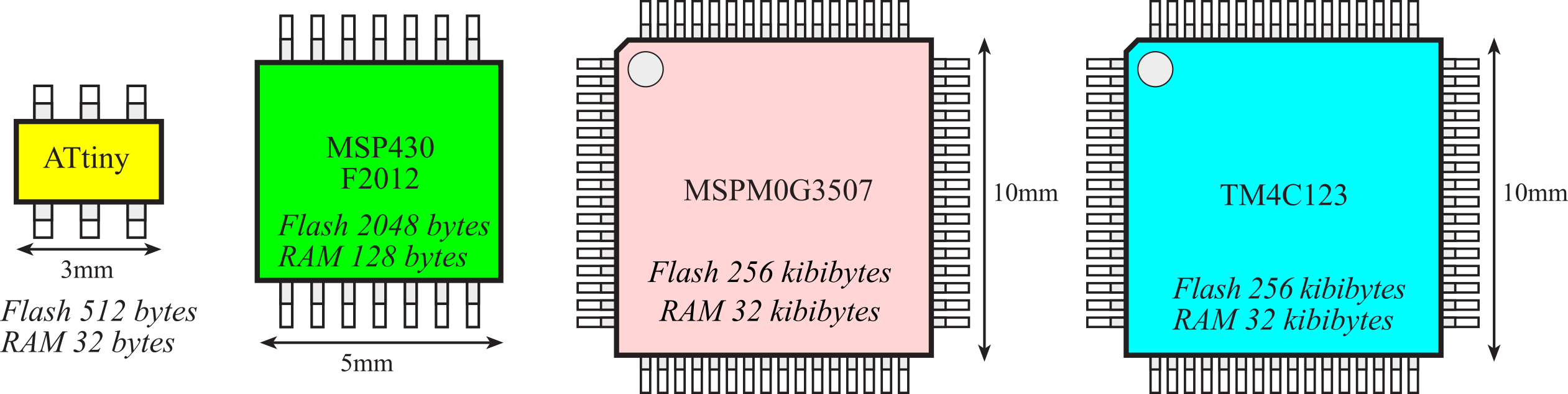
Figure 1.1.3. A microcontroller is a complete computer on a single chip.
Information is programmed into ROM using techniques more complicated than writing to RAM. From a programming viewpoint, retrieving data from a ROM is identical to retrieving data from RAM. ROMs are nonvolatile; meaning if power is interrupted and restored the information in the ROM is retained. Some ROMs are programmed at the factory and can never be changed. A Programmable ROM (PROM) can be erased and reprogrammed by the user, but the erase/program sequence is typically 10000 times slower than the time to write data into a RAM. PROMs used to need ultraviolet light to erase, and then we programmed them with voltages. Now, most PROMs now are electrically erasable (EEPROM), which means they can be both erased and programmed with voltages. We cannot program ones into the ROM. We first erase the ROM, which puts ones into its storage memory, and then we program the zeros as needed. Flash ROM is a popular type of EEPROM. Each flash bit requires only two MOSFET transistors. The input (gate) of one transistor is electrically isolated, so if we trap charge on this input, it will remain there for years. The other transistor is used to read the bit by sensing whether or not the other transistor has trapped charge. Flash ROM must be erased in large blocks. On the TM4C and MSPM0 microcontrollers, we can erase the entire ROM or just one 1024-byte sector. For all the systems in this book, we will store instructions and constants in flash ROM, and we will place variables and temporary data in static RAM.
: What are the differences between a microcomputer, a microprocessor and a microcontroller?
: Which has a higher information density on the chip in bits per mm2: static RAM or flash ROM? Assume all MOSFETs are approximately the same size in mm2.
Observation: Memory is an object that can transport information across time.
Observation: Bits in memory are stored as energy in J.
1.1.4. Types of Input/Output
Input/output devices are important in all computers, but they are especially significant in an embedded system. Connecting external devices to the microcontroller creating an embedded system will be the focus of this book. An input port is hardware on the microcontroller that allows information about the external world to be entered into the computer. The microcontroller also has hardware called an output port to send information out to the external world. Most of the pins shown in Figure 1.1.3 are input/output ports.
An interface is defined as the collection of the I/O port, external electronics, physical devices, and the software, which combines to allow the computer to communicate with the external world. An example of an input interface is a switch, where the operator toggles the switch, and the software can recognize the switch position. An example of an output interface is a light-emitting diode (LED), where the software can turn the light on and off, and the operator can see whether the light is shining. There is a wide range of possible inputs and outputs, which can exist in either digital or analog form. In general, we can classify I/O interfaces into four categories
Parallel - binary data are available simultaneously on a group of lines
Serial - binary data are available one bit at a time on a single line
Analog - data are encoded as an electrical voltage, current, or power
Time - data are encoded as a period, frequency, pulse width, or phase shift
Observation: The use of time as an input and an output has made a significant impact on the growth of embedded systems. Time is both less expensive and has higher performance than I/O based on voltage or current.
: What are the differences between an input port and an input interface?
The MSPM0G3507 has 2 ports: A and B. The TM4C123 has 6 ports: A, B, C, D, E, and F. However, both microcontrollers have 1000's of I/O registers used to configure and perform input output. See Appendix M. MSPM0 I/O and Appendix T. TM4C I/O. In a system with memory mapped I/O, as shown in Figures 1.1.1 and 1.1.2, the I/O registers are connected to the processor in a manner like memory. I/O registers are assigned addresses, and the software accesses I/O using reads and writes to the specific I/O addresses. The software inputs from an input port using the same instructions as it would if it were reading from memory. Similarly, the software outputs from an output port using the same instructions as it would if it were writing to memory.
Observation: Just to be clear, I/O registers are not memory. Some I/O bits are read only and some bits are write only. Please read the data sheets carefully to see how an I/O port acts.
In a computer system with I/O-mapped I/O, the control bus signals that activate the I/O are separate from those that activate the memory devices. These systems have a separate address space and separate instructions to access the I/O devices. The original Intel 8086 had four control bus signals MEMR, MEMW, IOR, and IOW. MEMR and MEMW were used to read and write memory, while IOR and IOW were used to read and write I/O. The Intel x86 refers to any of the processors that Intel has developed based on this original architecture. The Intel x86 processors continue to implement this separation between memory and I/O. Rather than use the regular memory access instructions, the Intel x86 processor uses special in and out instructions to access the I/O devices. The advantages of I/O-mapped I/O are that software cannot inadvertently access I/O when it thinks it is accessing memory. In other words, it protects I/O devices from common software bugs, such as bad pointers, stack overflow, and buffer overflows. In contrast, systems with memory-mapped I/O are easier to design, and the software is easier to write.
Observation: Most computers use memory-mapped I/O.
1.2. Cortex-M Architecture
1.2.1. Busses
The ARM Cortex-M processor has four major components, as illustrated in Figure 1.2.1. There are four bus interface units (BIU) that read data from the bus during a read cycle and write data onto the bus during a write cycle. Both the MSPM0 and TM4C123 microcontrollers support DMA. The BIU always drives the address bus and the control signals of the bus. The effective address register (EAR) contains the memory address used to fetch the data needed for the current instruction. Cortex-M microcontrollers execute Thumb instructions extended with Thumb-2 technology. Overviews of these instructions are presented in Cortex M4 Assembly and Cortex M0+ Assembly. The Cortex-M4F microcontrollers include a floating-point processor. However, in this book we will focus on integer and fixed-point arithmetic.

Figure 1.2.1. The four basic components of a processor.
The control unit (CU) orchestrates the sequence of operations in the processor. The CU issues commands to the other three components. The instruction register (IR) contains the operation code (or op code) for the current instruction. When extended with Thumb-2 technology, op codes are either 16 or 32 bits wide. In an embedded system the software is converted to machine code, which is a list of instructions, and stored in nonvolatile flash ROM. As instructions are fetched, they are placed in a pipeline. This allows instruction fetching to run ahead of execution. Instructions are fetched in order and executed in order. However, it can execute one instruction while fetching the next.
The registers are high-speed storage devices located in the processor (e.g., R0 to R15). Registers do not have addresses like regular memory, but rather they have specific functions explicitly defined by each instruction. Registers can contain data or addresses. The program counter (PC) points to the memory containing the instruction to execute next. On the ARM Cortex-M processor, the PC is register 15 (R15). In an embedded system, the PC usually points into nonvolatile memory like flash ROM. The information stored in nonvolatile memory (e.g., the instructions) is not lost when power is removed. The stack pointer (SP) points to the RAM, and defines the top of the stack. The stack implements last in first out (LIFO) storage. On the ARM Cortex-M processor, the SP is register 13 (R13). The stack is an extremely important component of software development, which can be used to pass parameters, save temporary information, and implement local variables. The program status register (PSR) contains the status of the previous operation, as well as some operating mode flags such as the interrupt enable bit.
The arithmetic logic unit (ALU) performs arithmetic and logic operations. Addition, subtraction, multiplication and division are examples of arithmetic operations. And, or, exclusive or, and shift are examples of logical operations.
: What do the acronyms CU DMA BIU ALU stand for?
In general, the execution of an instruction goes through four phases, see Table 1.2.1. First, the computer fetches the machine code for the instruction by reading the value in memory pointed to by the program counter (PC). Some instructions are 16 bits, while others are 32 bits. After each instruction is fetched, the PC is incremented to the next instruction. At this time, the instruction is decoded, and the effective address is determined (EAR). Many instructions require additional data, and during phase 2 the data is retrieved from memory at the effective address. Next, the actual function for this instruction is performed. During the last phase, the results are written back to memory. All instructions have a phase 1, but the other three phases may or may not occur for any specific instruction.
|
Phase |
Function |
Bus |
Address |
Comment |
|
1 |
Instruction fetch |
Read |
PC++ |
Put into IR |
|
2 |
Data read |
Read |
EAR |
Data passes through ALU |
|
3 |
Operation |
- |
- |
ALU operations, set PSR |
|
4 |
Data store |
Write |
EAR |
Results stored in memory |
Table 1.2.1. Four phases of execution.
On the ARM Cortex-M processor, an instruction may read memory or write memory, but it does not both read and write memory in the same instruction. Each of the phases may require one or more bus cycles to complete. Each bus cycle reads or writes one piece of data. Because of the multiple bus architecture, most instructions execute in one or two cycles. For more information on the time to execute instructions, see Table 3.1 in the Cortex-M Technical Reference Manual.
The Cortex M processor is a reduced instruction set computer (RISC), which achieves high performance by implementing very simple instructions that run extremely fast. An instruction on a RISC processor does not have both a phase 2 data read cycle and a phase 4 data write cycle. In general, a RISC processor has a small number of instructions, instructions have fixed lengths, instructions execute in 1 or 2 bus cycles, there are only a few instructions (e.g., load and store) that can access memory, no one instruction can both read and write memory in the same instruction, there are many identical general purpose registers, and there are a limited number of addressing modes.
Conversely, processors are classified as complex instruction set computers (CISC), because one instruction can perform multiple memory operations. For example, CISC processors have instructions that can both read and write memory in the same instruction. Assume Data is an 8-bit memory variable. The following Intel 8080 instruction will increment the 8-bit variable, requiring a read memory cycle, ALU operation, and then a write memory cycle.
INR Data ; Intel 8080
Other CISC processors like the 6800, 9S12, 8051, and Pentium also have memory increment instructions requiring both a phase 2 data read cycle and a phase 4 data write cycle. In general, a CISC processor has a large number of instructions, instructions have varying lengths, instructions execute in varying times, there are many instructions that can access memory, the processor can both read and write memory in one instruction, the processor has fewer and more specialized registers, and the processor has many addressing modes.
: What is the difference between CISC and RISC?
1.2.2. Registers
The registers are depicted in Figure 1.2.2. R0 to R12 are general purpose registers and contain either data or addresses. Register R13 (also called the stack pointer, SP) points to the top element of the stack. Actually, there are two stack pointers: the main stack pointer (MSP) and the process stack pointer (PSP). Only one stack pointer is active at a time. In a high-reliability operating system, we could activate the PSP for user software and the MSP for operating system software. This way the user program could crash without disturbing the operating system. Because of the simple and dedicated nature of the embedded systems developed in this book, we will exclusively use the main stack pointer. Register R14 (also called the link register, LR) is used to store the return location for functions. The LR is also used in a special way during exceptions, such as interrupts. Periodic interrupts will be presented in 1.9. SysTick Periodic Interrupts. Register R15 (also called the program counter, PC) points to the next instruction to be fetched from memory. The processor fetches an instruction using the PC and then increments the PC by 2 or 4.
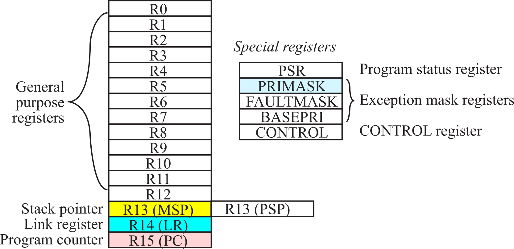
Figure 1.2.2. Registers on the ARM Cortex-M processor.
The ARM Architecture Procedure Call Standard, AAPCS, part of the ARM Application Binary Interface (ABI), uses registers R0, R1, R2, and R3 to pass input parameters into a C function. Also according to AAPCS we place the return parameter in Register R0.
There are three status registers named Application Program Status Register (APSR), the Interrupt Program Status Register (IPSR), and the Execution Program Status Register (EPSR) as shown in Figure 1.2.3. These registers can be accessed individually or in combination as the Program Status Register (PSR). The N, Z, V, C, and Q bits give information about the result of a previous ALU operation. In general, the N bit is set after an arithmetical or logical operation signifying whether or not the result is negative. Similarly, the Z bit is set if the result is zero. The C bit means carry and is set on an unsigned overflow, and the V bit signifies signed overflow. The Q bit is the sticky saturation flag, indicating that "saturation" has occurred, and is set by the SSAT and USAT instructions.
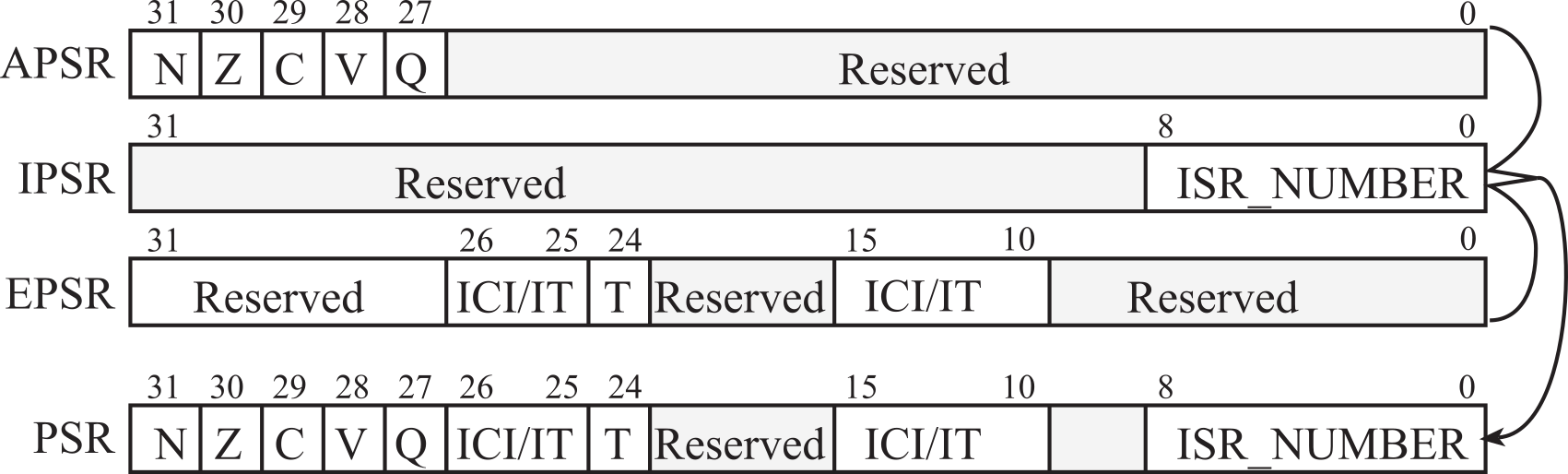
Figure 1.2.3. The program status register of the ARM Cortex-M processor.
The T bit will always be 1, indicating the ARM Cortex-M is executing Thumb instructions. The ICI/IT bits are used by interrupts and by the IF-THEN instructions. The ISR_NUMBER indicates which interrupt if any the processor is handling. Bit 0 of the special register PRIMASK is the interrupt mask bit. If this bit is 1 most interrupts and exceptions are not allowed. If the bit is 0, then interrupts are allowed. Bit 0 of the special register FAULTMASK is the fault mask bit. If this bit is 1 all interrupts and faults are not allowed. If the bit is 0, then interrupts and faults are allowed. The nonmaskable interrupt (NMI) is not affected by these mask bits. The BASEPRI register defines the priority of the executing software. It prevents interrupts with lower or equal priority but allows higher priority interrupts. For example if BASEPRI equals 3, then requests with level 0, 1, and 2 can interrupt, while requests at levels 3 and higher will be postponed. The details of interrupt processing will be presented in Chapter 5.
1.2.3. Memory and Bit banding
Microcontrollers within the same family differ by the amount of memory and by the types of I/O modules. All TM4C microcontrollers have a Cortex-M4 processor, floating point, CAN, DMA, USB, PWM, SysTick, RTC, timers, UART, I2C, SSI, and ADC. The TM4C1294NCPDT and MSP432E401Y also have Ethernet. There are hundreds of members in this family. The TM4C123 has 256 kibibytes (218 bytes) of flash ROM and 32 kibibytes (215 bytes) of RAM. The MSPM0G3507 has a CortexM0+ processor has 128 kibibytes (217 bytes) of flash ROM and 32 kibibytes (215 bytes) of RAM.
The memory map of TM4C123 is illustrated in Figure 1.2.4. All ARM Cortex-M microcontrollers have similar memory maps. In general, Flash ROM begins at address 0x00000000, RAM begins at 0x20000000, the peripheral I/O space is from 0x40000000 to 0x5FFFFFFF, and I/O modules on the private peripheral bus exist from 0xE0000000 to 0xE00FFFFF. In particular, the only differences in the memory map for the various members of the TM4C families are the ending addresses of the flash and RAM. Having multiple buses means the processor can perform multiple tasks in parallel. The following is some of the tasks that can occur in parallel
ICode bus Fetch opcode from ROM
DCode bus Read constant data from ROM
System bus Read/write data from RAM or I/O, fetch opcode from RAM
PPB Read/write data from internal peripherals like the NVIC
AHB Read/write data from high-speed I/O and parallel ports (M4 only)
The ARM Cortex-M4 uses bit-banding to allow read/write access to individual bits in RAM and some bits in the I/O space. There are two parameters that define bit-banding: the address and the bit you wish to access. Assume you wish to access bit b of RAM address 0x2000.0000+n, where b is a number 0 to 7. The aliased address for this bit will be
0x2200.0000 + 32*n + 4*b
Reading this address will return a 0 or a 1. Writing a 0 or 1 to this address will perform an atomic read-modify-write modification to the bit.
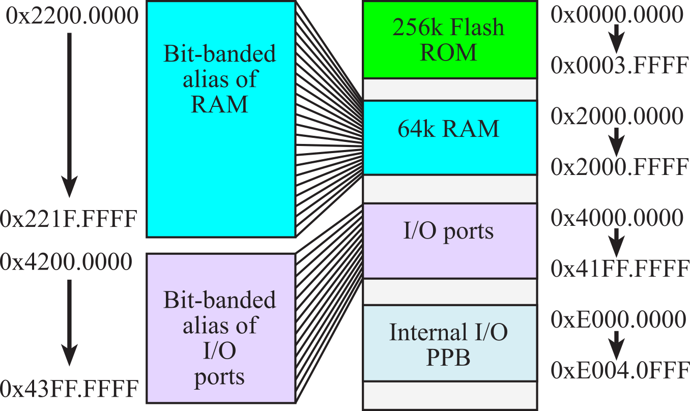
Figure 1.2.4a. Memory map of the TM4C123.
If we consider 32-bit word-aligned data in RAM, the same bit-banding formula still applies. Let the word address be 0x20000000+n. n starts at 0 and increments by 4. In this case, we define b as the bit from 0 to 31. In little-endian format, bit 1 of the byte at 0x20000001 is the same as bit 9 of the word at 0x20000000. The aliased address for this bit will still be
0x22000000 + 32*n + 4*b
Examples of bit-banded addressing are listed in Table 1.2.2. Writing a 1 to location 0x22000018 will set bit 6 of RAM location 0x20000000. Reading location 0x22000024 will return a 0 or 1 depending on the value of bit 1 of RAM location 0x20000001.
|
RAM address |
Offset n |
Bit b |
Bit-banded alias |
|
0x20000000 |
0 |
0 |
0x22000000 |
|
0x20000000 |
0 |
1 |
0x22000004 |
|
0x20000000 |
0 |
2 |
0x22000008 |
|
0x20000000 |
0 |
3 |
0x2200000C |
|
0x20000000 |
0 |
4 |
0x22000010 |
|
0x20000000 |
0 |
5 |
0x22000014 |
|
0x20000000 |
0 |
6 |
0x22000018 |
|
0x20000000 |
0 |
7 |
0x2200001C |
|
0x20000001 |
1 |
0 |
0x22000020 |
|
0x20000001 |
1 |
1 |
0x22000024 |
Table 1.2.2. Examples of bit-banded addressing.
: What address do you use to access bit 5 of the byte at 0x20001003?
: What address do you use to access bit 20 of the word at 0x20001000?
The other bit-banding region is the I/O space from 0x40000000 through 0x400F.FFFF. In this region, let the I/O address be 0x40000000+n, and let b represent the bit 0 to 7. The aliased address for this bit will be
0x42000000 + 32*n + 4*b
: What address do you use to access bit 2 of the byte at 0x40000003?
The memory map of MSPM0G3507 is
illustrated in Figure 1.2.4b. All MSPM0 microcontrollers have similar memory
maps. In general, Flash ROM begins at address 0x00000000, RAM begins at
0x20200000, the peripheral I/O space begins at 0x40000000, and ARM specific I/O
begins at 0xE0000000. In
particular, the only differences in the memory map for the various members of
the MSPM0 families are the ending addresses of the flash and RAM.
The MSPM0 does not support bit-banding.

Figure 1.2.4b. Memory map of the MSPM0G3507.
1.2.4. Stack
The stack is a last-in-first-out temporary storage. To create a stack, a block of RAM is allocated for this temporary storage. On the ARM Cortex-M, the stack always operates on 32-bit data. The stack pointer (SP) points to the 32-bit data on the top of the stack. The stack grows downwards in memory as we push data on to it so, although we refer to the most recent item as the "top of the stack" it is actually the item stored at the lowest address! To push data on the stack, the stack pointer is first decremented by 4, and then the 32-bit information is stored at the address specified by SP. To pop data from the stack, the 32-bit information pointed to by SP is first retrieved, and then the stack pointer is incremented by 4. SP points to the last item pushed, which will also be the next item to be popped. The processor allows for two stacks, the main stack and the process stack, with two independent copies of the stack pointer. The boxes in Figure 1.2.5 represent 32-bit storage elements in RAM. The grey boxes in the figure refer to actual data stored on the stack, and the white boxes refer to locations in memory that do not contain stack data. This figure illustrates how the stack is used to push the contents of Registers R0, R1, and R2 in that order. Assume Register R0 initially contains the value 1, R1 contains 2 and R2 contains 3. The drawing on the left shows the initial stack. The software executes these six instructions
PUSH {R0}
PUSH {R1}
PUSH {R2}
POP {R3}
POP {R4}
POP {R5}
The instruction PUSH {R0} saves the value of R0 on the stack. It first decrements SP by 4, and then it stores the 32-bit contents of R0 into the memory location pointed to by SP. The four bytes are stored little endian. The right-most drawing shows the stack after the push occurs three times. The stack contains the numbers 1 2 and 3, with 3 on top.
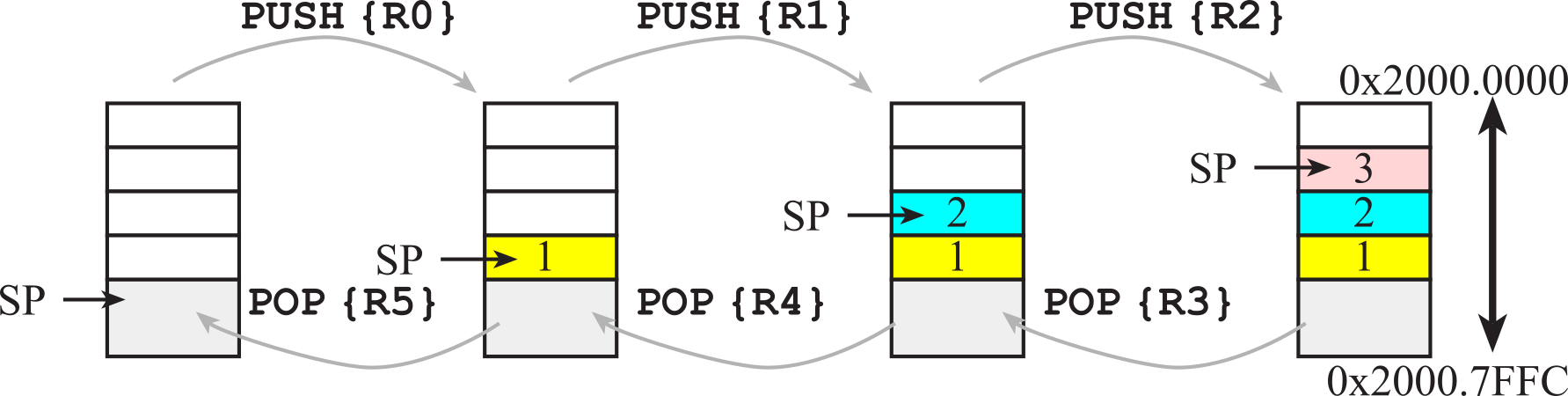
Figure 1.2.5. Stack picture showing three numbers first being pushed, then three numbers being popped.
The instruction POP
{R3} retrieves data from the stack. It first moves the value from
memory pointed to by SP into R3, and then it increments SP by 4. After the pop
occurs three times the stack reverts to its original state and registers R3, R4
and R5 contain 3 2 1 respectively. We define the 32-bit word pointed to by SP
as the top entry of the stack. If it exists, we define the 32-bit data
immediately below the top, at SP+4, as next to top. Proper use of the
stack requires following these important rules
- Functions should have an equal number of pushes and pops
- Stack accesses (push or pop) should not occur outside the allocated area
- Stack reads and writes should not be performed within the free area
- Stack push should first decrement SP, then store the data
- Stack pop should first read the data, and then increment SP
Functions that violate rule number 1 will probably crash when incorrect data are popped off at a later time. Violations of rule number 2 can be caused by a stack underflow or overflow. Overflow occurs when the number of elements becomes larger than the allocated space. Stack underflow is caused when there are more pops than pushes, and is always the result of a software bug. A stack overflow can be caused by two reasons. If the software mistakenly pushes more than it pops, then the stack pointer will eventually overflow its bounds. Even when there is exactly one pop for each push, a stack overflow can occur if the stack is not allocated large enough. The processor will generate a bus fault when the software tries read from or write to an address that doesn't exist. If valid RAM exists below the stack then pushing to an overflowed stack will corrupt data in this memory.
Executing an interrupt service routine will automatically push information on the stack. Since interrupts are triggered by hardware events, exactly when they occur is not under software control. Therefore, violations of rules 3, 4, and 5 will cause erratic behavior when operating with interrupts. Rules 4 and 5 are followed automatically by the PUSH and POP instructions.
1.2.5. Operating modes
The ARM Cortex-M has two privilege levels called privileged and unprivileged. Bit 0 of the CONTROL register is the thread mode privilege level (TPL). If TPL is 1 the processor level is privileged. If the bit is 0, then processor level is unprivileged. Running at the unprivileged level prevents access to various features, including the system timer and the interrupt controller. Bit 1 of the CONTROL register is the active stack pointer selection (ASPSEL). If ASPSEL is 1, the processor uses the PSP for its stack pointer. If ASPSEL is 0, the MSP is used. When designing a high-reliability operating system, we will run the user code at an unprivileged level using the PSP and the OS code at the privileged level using the MSP.
The processor knows whether it is running in the foreground (i.e., the main program) or in the background (i.e., an interrupt service routine). ARM defines the foreground as thread mode, and the background as handler mode. Switching from thread mode to handler mode occurs when an interrupt is triggered. The processor begins in thread mode, signified by ISR_NUMBER=0. Whenever it is servicing an interrupt it switches to handler mode, signified by setting ISR_NUMBER to specify which interrupt is being processed. All interrupt service routines run using the MSP. At the end of the interrupt service routine the processor is switched back to thread mode, and the main program continues from where it left off.
1.2.6. Reset
A reset occurs immediately after power is applied and can also occur by pushing the reset button available on most boards. After a reset, the processor is in thread mode, running at a privileged level, and using the MSP stack pointer. The 32-bit value at flash ROM location 0 is loaded into the SP. All stack accesses are word aligned. Thus, the least significant two bits of SP must be 0. A reset also loads the 32-bit value at location 4 into the PC. This value is called the reset vector. All instructions are halfword-aligned. Thus, the least significant bit of PC must be 0. However, the assembler will set the least significant bit in the reset vector, so the processor will properly initialize the thumb bit (T) in the PSR. On the ARM Cortex-M, the T bit should always be set to 1. On reset, the processor initializes the LR to 0xFFFFFFFF.
1.3. Embedded Systems
1.3.1. Definition and Characteristics
An embedded system is an electronic system that includes one or more microcontrollers that are configured to perform a specific dedicated application, drawn previously as Figure 1.1.2. To better understand the expression "embedded system", consider each word separately. In this context, the word embedded means "a computer is hidden inside so one can't see it." The word "system" refers to the fact that there are many components which act in concert achieving the common goal. When a user holds an embedded system they see it as a smart device, rather than a computer, allowing them to interact with the real world.
A user asks, "How does it do that?" The answer is, "It has a computer inside". The software that controls the system is programmed or fixed into flash ROM and is not accessible to the user of the device. Even so, software maintenance is still extremely important. Maintenance is verification of proper operation, updates, fixing bugs, adding features, and extending to new applications and end user configurations. Embedded systems have these four characteristics.
First, embedded systems typically solve a single objective. Consequently, they solve a limited range of problems. For example, the embedded system in a microwave oven may be reconfigured to control different versions of the oven within a similar product line. But, a microwave oven will always be a microwave oven, and you can't reprogram it to be a dishwasher. Embedded systems are unique because of the microcontroller's I/O ports to which the external devices are interfaced. This allows the system to interact with the real world.
Second, embedded systems are tightly constrained. Typically, system must operate within very specific performance parameters. If an embedded system cannot operate with specifications, it is considered a failure and will not be sold. For example, a cell-phone carrier typically gets 832 radio frequencies to use in a city, a hand-held video game must cost less than $50, an automotive cruise control system must operate the vehicle within 3 mph of the set-point speed, and a portable MP3 player must operate for 12 hours on one battery charge.
Third, many embedded systems must operate in real-time. In a real-time system, we can put an upper bound on the time required to perform the input-calculation-output sequence. A real-time system can guarantee a worst case upper bound on the response time between when the new input information becomes available and when that information is processed. Another real-time requirement that exists in many embedded systems is the execution of periodic tasks. A periodic task is one that must be performed at equal time intervals. A real-time system can put a small and bounded limit on the time error between when a task should be run and when it is actually run. Because of the real-time nature of these systems, microcontrollers in the TM4C family have a rich set of features to handle all aspects of time.
The fourth characteristic of embedded systems is their small memory requirements as compared to general purpose computers. There are exceptions to this rule, such as those which process video or audio, but most have memory requirements measured in thousands of bytes. Over the years, the memory in embedded systems has increased, but the gap in memory size between embedded systems and general-purpose computers remains. The original microcontrollers had thousands of bytes of memory, and the PC had millions. Now, microcontrollers can have millions of bytes, but the PC has billions.
1.3.2. Abstraction
There have been two trends in the microcontroller field. The first trend is to make microcontrollers smaller, cheaper, and lower power. The Atmel ATtiny, Microchip PIC, and Texas Instruments MSP430 families are good examples of this trend. Size, cost, and power are critical factors for high-volume products, where the products are often disposable. On the other end of the spectrum is the trend of larger RAM and ROM, faster processing, and increasing integration of complex I/O devices, such as Ethernet, radio, graphics, and audio. It is common for one device to have multiple microcontrollers, where the operational tasks are distributed, and the microcontrollers are connected in a local area network (LAN). These high-end features are critical for consumer electronics, medical devices, automotive controllers, and military hardware, where performance and reliability are more important than cost. However, small size and low power continue as important features for all embedded systems.
To deal with increasing complexity, embedded system design deploys abstraction, which is the process of hiding the physical/spatial/temporal details and focusing on high-level functionality. For example, we can learn to drive a car without knowing how a car works. The automobile manufacturer provides user interfaces (steering wheel, gas pedal, and brake) that we use to control the car. Underneath, the engineers design the system to convert high-level functionality into low-level inputs and outputs. There are many abstractive design methods presented in this book. Figure 1.3.1 shows four embedded system abstractions, with varying levels of functionality exposed to the user. Basic embedded systems hide all software and hardware (e.g., motor controller). Firmware is the low-level software that directly interacts with hardware. Another name for firmware is I/O drivers. An operating system (OS) is software that manages the resources (I/O, time, data) within the system. Embedded systems do no run Windows or MacOS, but may run specialized OSs like Linux, Windows IoT, Android OS or iOS. Real-time operating systems (RTOS), presented in Volume 3, guarantee important tasks will be performed on time. Complex embedded systems have multiple software layers: application software, operating system, and firmware (e.g., digital video recorder). Cellphones are a class of embedded systems that expose some software to the user. The iPhone only exposes application software. Conversely, an Android phone exposes more of the software to the user. In each case, the abstraction of each layer in Figure 1.3.1 defines what the layer does, hiding the details of how it works.
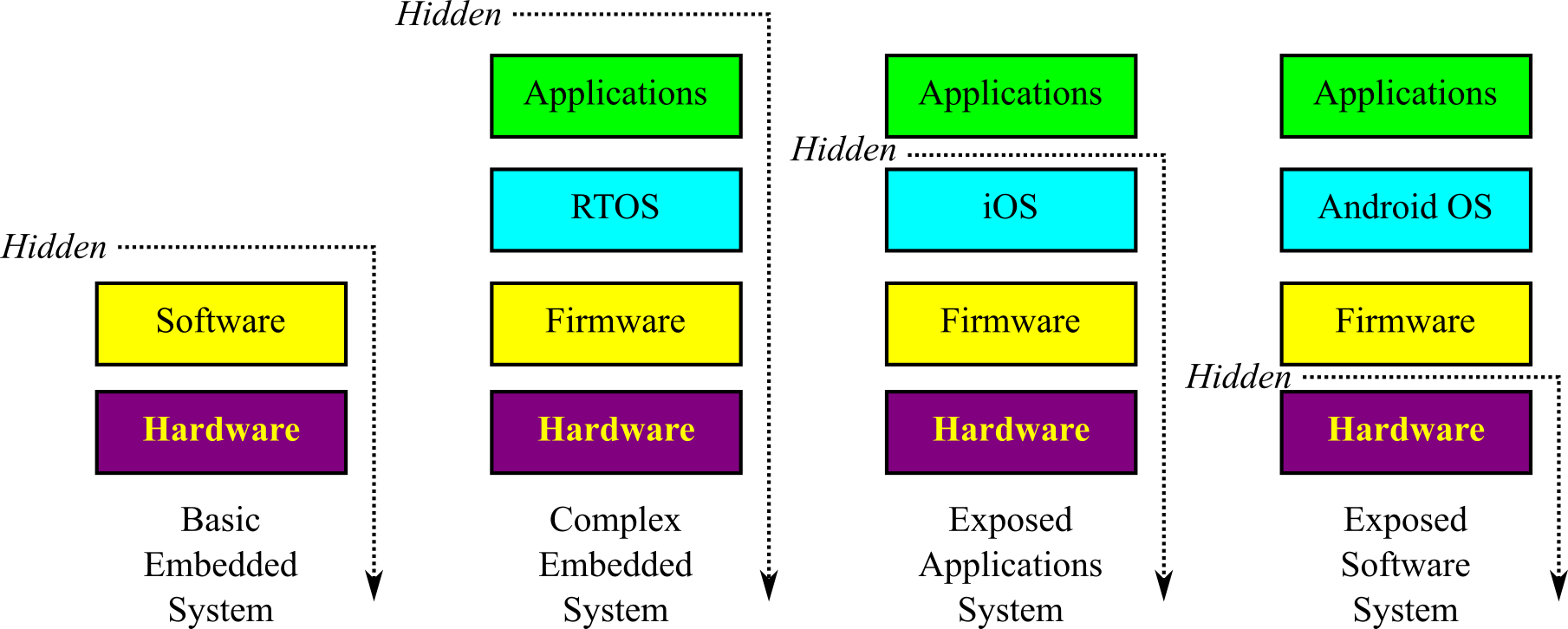
Figure 1.3.1. Embedded system abstractions.
Abstraction occurs both at the software level, like shown in Figure 1.3.1, and at the hardware level. All I/O devices presented in the book allow for hardware abstraction. In addition, the differentiation between hardware and software is blurry. The use of field programmable gate arrays (FPGA) creates components that have properties of both hardware and software.
1.3.3. Interfaces
Interfaces allow various hardware and software components of a system to interact with each other. Interface design, which is a major focus of this book, is a critical factor when developing complex systems.
The RAM is volatile memory, meaning its information is lost when power is removed. On some embedded systems a battery powers the microcontroller. When in the off mode, the microcontroller goes into low-power sleep mode, which means the information in RAM is maintained, but the processor is not executing. The MSPM0 requires less than one µA of current in sleep mode.
: What is an embedded system?
: What goes in the RAM on a smartphone?
: Why does your smartphone need so much flash ROM?
The computer engineer has many design choices to make when building a real-time embedded system. Often, defining the problem, specifying the objectives, and identifying the constraints are harder than actual implementations. In this book, we will develop computer engineering design processes by introducing fundamental methodologies for problem specification, prototyping, testing, and performance evaluation.
A typical automobile now contains an average of ten
microcontrollers. In fact, upscale homes may contain as many as 150
microcontrollers and the average consumer now interacts with microcontrollers
up to 300 times a day. The general areas that employ embedded systems encompass
every field of engineering:
- Consumer electronics, wearables
- Home
- Communications
- Automotive
- Military
- Industrial
- Business
- Shipping
- Medical
- Computer components
In general, embedded systems have inputs, perform calculations, make decisions, and then produce outputs. The microcontrollers often must communicate with each other. How the system interacts with humans is often called the human-computer interface (HCI) or man-machine interface (MMI).
There are over dozens of sensors in a cellphone, see Table 1.3.1.
|
Sensor |
Measurand |
|
Light |
Light intensity |
|
9-axis IMU |
Motion |
|
3+ Camera |
Images |
|
4+ Microphone |
Sounds |
|
Touch |
User input |
|
GPS |
Position |
|
Antennae |
Wi-fi, cellular, Bluetooth |
|
Coils |
NFC |
|
Fingerprint |
Identifies user |
|
Proximity |
Distance to object |
|
Pressure |
Atomspheric pressure |
|
Environmental |
Temperature, humidity |
Table 1.3.1. Sensors in a typical cellphone.
The I/O interfaces are a crucial part of an embedded system because they provide necessary functionality. Most personal computers have the same basic I/O devices (e.g., mouse, keyboard, video display, CD, USB, and hard drive.) In contrast, there is no common set of I/O that all embedded system have. The software together with the I/O ports and associated interface circuits give an embedded computer system its distinctive characteristics. A device driver is a set of software functions that facilitate the use of an I/O port. Another name for device driver is application programmer interface (API).
When designing embedded systems, we need to know how to
interface a wide range of signals that can exist in digital, analog, or time
formats. Parallel ports provide for digital input and outputs. Serial ports
employ a wide range of formats and synchronization protocols. The serial ports
can communicate with devices such as:
- Sensors
- Liquid Crystal Displays (LCD)
- Analog to digital converters (ADC)
- Digital to analog converters (DAC)
- Wireless devices like Bluetooth, ZigBee and Wifi.
Analog to digital converters convert analog voltages to
digital numbers. Digital to analog converters convert digital numbers to analog
voltages. The timer features include:
- Fixed rate periodic execution
- Square wave and Pulse Width Modulated outputs (PWM)
- Input capture used for period, frequency and pulse width measurement
: List three input interfaces available on a smart watch.
: List three output interfaces available on a smart thermostat.
1.3.4. Examples
Table 1.3.2 lists example products and the functions performed by their embedded systems. The microcontroller accepts inputs, performs calculations, and generates outputs.
Functions
performed by the microcontroller
Consumer/Home:
Washing machine Controls
the water and spin cycles, saving water and energy
Wearables Measures speed, distance, calories, heart rate,
wireless communication
Remote controls Accepts
key touches, sends infrared pulses, learns how to interact with user
Clocks and
watches Maintains the time, alarm, and display
Games and toys Entertains
the user, joystick input, video output
Audio/video Interacts
with the operator, enhances performance with sounds and pictures
Set-back
thermostats Adjusts day/night thresholds saving energy
Communication:
Answering
machines Plays outgoing messages and saves incoming messages
Telephone
system Switches signals and retrieves information
Cellular phones Interacts
with touch screen, microphone, accelerometer,
GPS, and speaker
Internet
of things Sends and receives messages with
other computers around the world
Automotive:
Automatic
braking Optimizes stopping on slippery surfaces
Noise
cancellation Improves sound quality, removing noise
Theft deterrent
devices Allows keyless entry, controls alarm
Electronic
ignition Controls sparks and fuel injectors
Windows and
seats Remembers preferred settings for each driver
Instrumentation Collects
and provides necessary information
Military:
Smart weapons Recognizes
friendly targets
Missile
guidance Directs ordnance at the desired target
Global
positioning Determines where you are on the planet, suggests paths,
coordinates troops
Surveillance Collects
information about enemy activities
Industrial/Business/Shipping:
Point-of-sale
systems Accepts inputs and manages money, keeps credit information secure
Temperature
control Adjusts heating and cooling to maintain temperature
Robot systems Inputs
from sensors, controls the motors improving productivity
Inventory
systems Reads and prints labels, maximizing profit, minimizing shipping
delay
Automatic
sprinklers Controls the wetness of the soil maximizing plant growth
Medical:
Infant apnea
monitors Detects breathing, alarms if stopped
Cardiac
monitors Measures heart function, alarms if problem
Cancer
treatments Controls doses of radiation, drugs, or heat
Prosthetic
devices Increases mobility for the handicapped
Medical records Collect,
organize, and present medical information
Computer
Components:
Mouse Translates
hand movements into commands for the main computer
USB flash drive Facilitates
the storage and retrieval of information
Keyboard Accepts
key strokes, decodes them, and transmits to the main computer
Table 1.3.2. Products involving embedded systems.
To get a sense of what "embedded system" means we will present brief descriptions of four example systems.
Example 1.3.1: The goal of a pacemaker is to regulate and improve heart function. To be successful the engineer must understand how the heart works and how disease states cause the heart to fail. Its inputs are sensors on the heart to detect electrical activity, and its outputs can deliver electrical pulses to stimulate the heart. Consider a simple pacemaker with two sensors, one in the right atrium and the other in the right ventricle. The sensor allows the pacemaker to know if the normal heart contraction is occurring. This pacemaker has one right ventricular stimulation output. The embedded system analyzes the status of the heart deciding where and when to send simulation pulses. If the pacemaker recognizes the normal behavior of atrial contraction followed shortly by ventricular contraction, then it will not stimulate. If the pacemaker recognizes atrial contraction without a following ventricular contraction, then is will pace the ventricle shortly after each atrial contraction. If the pacemaker senses no contractions or if the contractions are too slow, then it can pace the ventricle at a regular rate. A pacemaker can also communicate via radio with the doctor to download past performance and optimize parameters for future operation. Some pacemakers can call the doctor on the phone when it senses a critical problem. Pacemakers are real-time systems because the time delay between atrial sensing and ventricular triggering is critical. Low power and reliability are important.
Example 1.3.2: The goal of a smoke detector is to warn people in the event of a fire. It has two inputs. One is a chemical sensor that detects the presence of smoke, and the other is a button that the operator can push to test the battery. There are also two outputs: an LED and the alarm. Most of the time, the detector is in a low-power sleep mode. If the test button is pushed, the detector performs a self-diagnostic and issues a short sound if the sensor and battery are ok. Once every 30 seconds, it wakes up and checks to see if it senses smoke. If it senses smoke, it will alarm. Otherwise, it goes back to sleep. Advanced smoke detectors should be able to communicate with other devices in the home. If one sensor detects smoke, all alarms should sound. If multiple detectors in the house collectively agree there is really a fire, they could communicate with the fire department and with the neighboring houses. To design and deploy a collection of detectors, the engineer must understand how fires start and how they spread. Smoke detectors are not real-time systems. However, reliability and low power are important.
Example 1.3.3: The goal of a motor controller is to cause a motor to spin in a desired manner. Sometimes we control speed, as in the cruise control on an automobile. Sometimes we control position as in moving paper through a printer. In a complex robotics system, we may need to simultaneously control multiple motors and multiple parameters such as position, speed, and torque. Torque control is important for building a robot that walks. The engineer must understand the mechanics of how the motor interacts with its world and the behavior of the interface electronics. The motor controller uses sensors to measure the current state of the motor, such as position, speed, and torque. The controller accepts input commands defining the desired operation. The system uses actuators, which are outputs that affect the motor. A typical actuator allows the system to set the electrical power delivered to the motor. Periodically, the microcontroller senses the inputs and calculates the power needed to minimize the difference between measured and desired parameters. This needed power is output to the actuator. Motor controllers are real-time systems, because performance depends greatly on when and how fast the controller software runs. Accuracy, stability, and time are important.
Example 1.3.4: The goal of a traffic light controller is to minimize waiting time and to save energy. The engineer must understand the civil engineering of how city streets are laid out and the behavior of human drivers as they interact with traffic lights and other drivers. The controller uses sensors to know the number of cars traveling on each segment of the road. Pedestrians can also push walk buttons. The controller will accept input commands from the fire or police department to handle emergencies. The outputs are the traffic lights at each intersection. The controller collects sensor inputs and calculates the traffic pattern needed to minimize waiting time, while maintaining safety. Traffic controllers are not real-time systems, because human safety is not sacrificed if a request is delayed. In contrast, an air traffic controller must run in real time, because safety is compromised if a response to a request is delayed. The system must be able to operate under extreme conditions such as rain, snow, freezing temperature, and power outages. Computational speed and sensor/light reliability are important.
: There is a microcontroller embedded in an alarm clock. List three operations the software must perform.
1.3.5. Internet of Things
The internet of things (IoT)
can broadly be defined as multiple embedded systems (the things) connected
together (the internet), see Figure 1.3.2. The applications in Table 1.3.1
describe a single device with dedicated purpose. However, we can create a
distributed system by connecting them together via the internet. In
Chapter 4. Internet of Things, we will study protocols Ethernet, wifi, subGHz,
and Bluetooth Low Energy (BLE). Since 2014, IoT has experienced explosive
growth, and all projections predict this growth to continue. IoT has
transformed all sectors that utilize computer systems including:
- Industrial and manufacturing
- Consumer electronics
- Retail, finance, and marketing
- Healthcare
- Transportation and logistics
- Agriculture and environment
- Energy production, storage, distribution, and marketing
- Smart cities
- Military
- Government
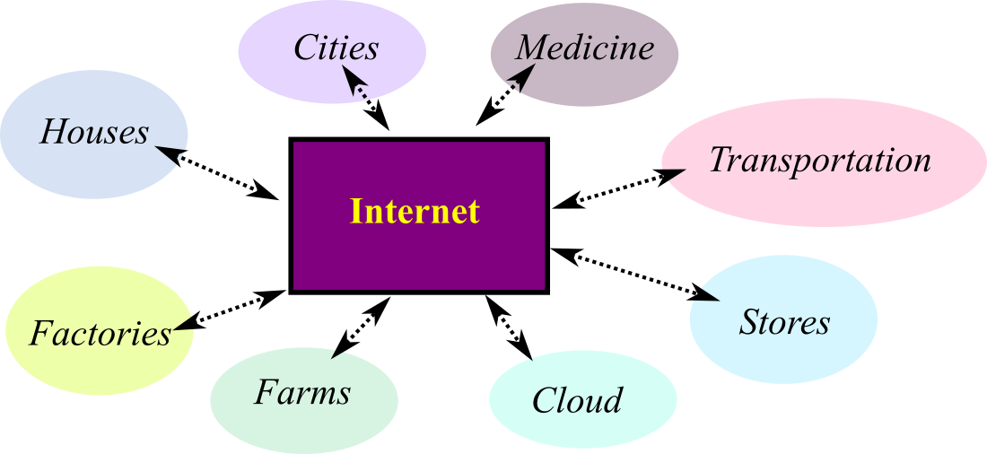
Figure 1.3.2. The internet of things connect devices together.
1.4. The Design Process
1.4.1. Requirements document
Before beginning any project, it is a good idea to have a plan. The following is one possible outline of a requirements document. Although originally proposed for software projects, it is appropriate to use when planning an embedded system, which includes software, electronics, and mechanical components. IEEE publishes a number of templates that can be used to define a project (IEEE STD 830-1998). A requirements document states what the system will do. It does not state how the system will do it. The main purpose of a requirements document is to serve as an agreement between you and your clients describing what the system will do. This agreement can become a legally binding contract. Write the document so that it is easy to read and understand by others. It should be unambiguous, complete, verifiable, and modifiable.
The requirements document should not include how the system will be designed. This allows the engineer to make choices during the design to minimize cost and maximize performance. Rather it should describe the problem being solved and what the system actually does. It can include some constraints placed on the development process. Ideally, it is co-written by both the engineers and the non-technical clients. However, it is imperative that both the engineers and the clients understand and agree on the specifics in the document.
1. Overview
1.1. Objectives: Why are we doing this
project? What is the purpose?
1.2. Process: How will the project be
developed?
1.3. Roles and Responsibilities: Who
will do what? Who are the clients?
1.4. Interactions with Existing
Systems: How will it fit in?
1.5. Terminology: Define terms used in
the document.
1.6. Security: How will intellectual
property be managed?
2. Function Description
2.1. Functionality: What will the
system do precisely?
2.2. Scope: List the phases and what
will be delivered in each phase.
2.3. Prototypes: How will intermediate
progress be demonstrated?
2.4. Performance: Define the measures
and describe how they will be determined.
2.5. Usability: Describe the
interfaces. Be quantitative if possible.
2.6. Safety: Explain any safety
requirements and how they will be measured.
3. Deliverables
3.1. Reports: How will the system be
described?
3.2. Audits: How will the clients
evaluate progress?
3.3. Outcomes: What are the
deliverables? How do we know when it is done?
Observation: To build a system without a requirements document means you are never wrong, but never done.
1.4.2. Top-down design
In this section, we will present the top-down design process. The process is called top-down, because we start with the high-level designs and work down to low-level implementations. The basic approach is introduced here, and the details of these concepts will be presented throughout the remaining chapters of the book. As we learn software/hardware development tools and techniques, we can place them into the framework presented in this section. As illustrated in Figure 1.4.1, the development of a product follows an analysis-design-implementation-testing cycle. For complex systems with long life-spans, we traverse multiple times around the development cycle. For simple systems, a one-time pass may suffice. Even after a system is deployed, it can reenter the life cycle to add features or correct mistakes.
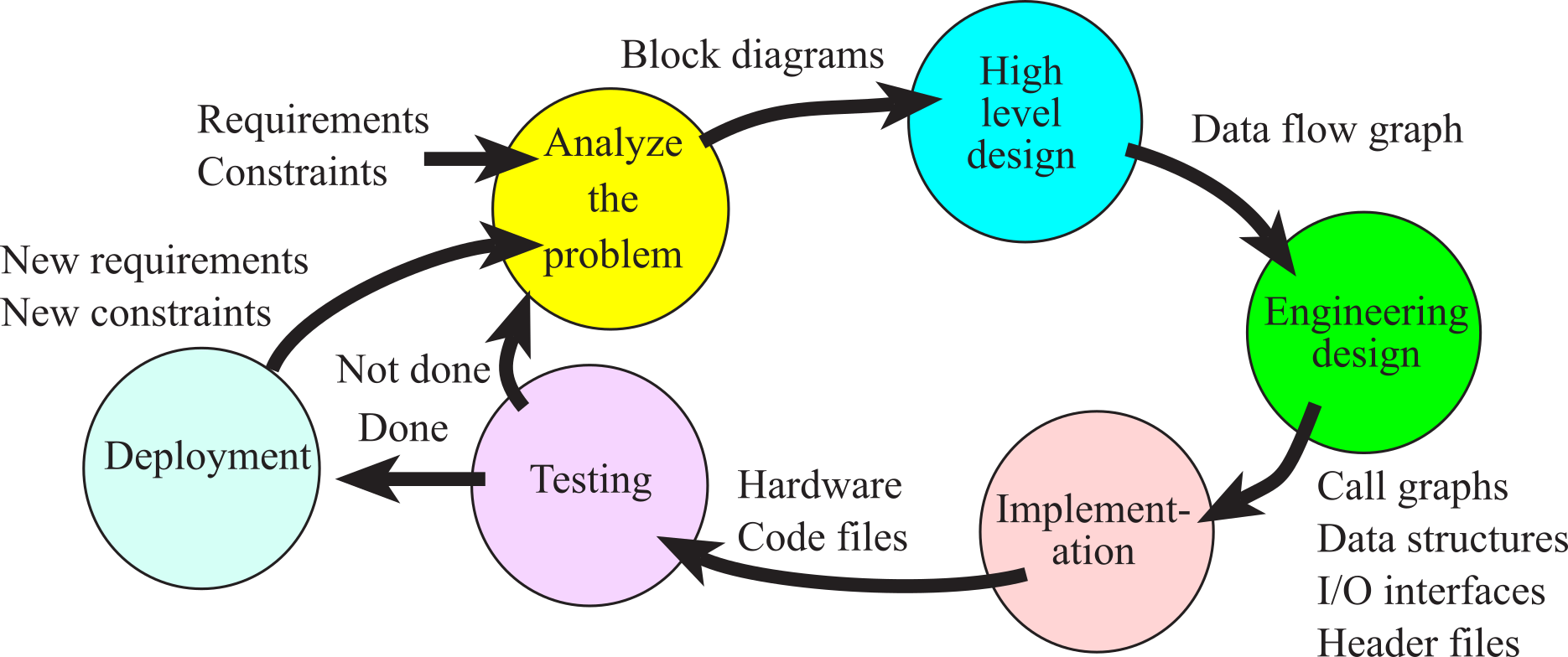
Figure 1.4.1. System development cycle or life-cycle. After the system is done it can be deployed.
During the analysis phase, we discover the
requirements and constraints for our proposed system. We can hire consultants
and interview potential customers in order to gather this critical information.
A requirement is a specific parameter that the system must satisfy,
describing what the system should do. We begin by rewriting the system
requirements, which are usually written as a requirements document. In general,
specifications are detailed parameters describing how the system should
work. For example, a requirement may state that the system should fit into a
pocket, whereas a specification would give the exact size and weight of the
device. For example, suppose we wish to build a motor controller. During the
analysis phase, we would determine obvious specifications such as range,
stability, accuracy, and response time. The following measures are often
considered during the analysis phase:
Safety: The risk to humans or the
environment
Accuracy: The difference between the
expected truth and the actual
parameter
Precision: The number of distinguishable
measurements
Resolution: The smallest change that can
be reliably detected
Response time: The time between a triggering event and the resulting action
Bandwidth: The amount of information
processed per time
Signal to noise ratio: The quotient of
the signal amplitude divided by the noise
Maintainability: The flexibility with
which the device can be modified
Testability: The ease with which proper
operation of the device can be verified
Compatibility: The conformance of the
device to existing standards
Mean time between failure: The
reliability of the device defining the life if a product
Size and weight: The physical space
required by the system and its mass
Power: The amount of energy it takes to
operate the system
Nonrecurring engineering cost (NRE cost):
The one-time cost to design and test
Unit cost: The cost required to
manufacture one additional product
Time-to-prototype: The time required to
design build and test an example system
Time-to-market: The time required to
deliver the product to the customer
Human factors: The degree to which our
customers enjoy/like/appreciate the product
There are many parameters to consider, and their relative importance may be difficult to ascertain. For example, in consumer electronics the human interface can be more important than bandwidth or signal to noise ratio. Often, improving performance on one parameter can be achieved only by decreasing the performance of another. This art of compromise defines the tradeoffs an engineer must make when designing a product. A constraint is a limitation, within which the system must operate. The system may be constrained to such factors as cost, safety, compatibility with other products, use of specific electronic and mechanical parts as other devices, interfaces with other instruments and test equipment, and development schedule.
: What's the difference between a requirement and a specification?
When you write a paper, you first decide on a theme, and next you write an outline. In the same manner, if you design an embedded system, you define its specification (what it does) and begin with an organizational plan. In this section, we will present three graphical tools to describe the organization of an embedded system: data flow graphs, call graphs, and flowcharts. You should draw all three for every system you design.
During the high-level design phase, we build a conceptual model of the hardware/software system. It is in this model that we exploit as much abstraction as appropriate. The project is broken in modules or subcomponents. Modular design will be presented in Chapter 7. System Design. During this phase, we estimate the cost, schedule, and expected performance of the system. At this point we can decide if the project has a high enough potential for profit. A data flow graph is a block diagram of the system, showing the flow of information. Arrows point from source to destination. It is good practice to label the arrows with the information type and bandwidth. The rectangles represent hardware components and the ovals are software modules. We use data flow graphs in the high-level design, because they describe the overall operation of the system while hiding the details of how it works. Issues such as safety (e.g., Isaac Asimov's first Law of Robotics "A robot may not harm a human being, or, through inaction, allow a human being to come to harm") and testing (e.g., we need to verify our system is operational) should be addressed during the high-level design.
An example data flow graph for a motor controller is shown in Figure 1.4.2. Notice that the arrows are labeled with data type and bandwidth. The requirement of the system is to deliver power to a motor so that the speed of the motor equals the desired value set by the operator using a keypad. In order to make the system easier to use and to assist in testing, a liquid crystal display (LCD) is added. The tachometer converts motor speed an electrical signal. The threshold detector converts this electrical signal into a digital signal with a frequency proportional to the motor speed. The timer capture hardware measures the period of this wave. The timer software, using mathematical functions, converts raw timing data into measured motor speed. The user will be able to select the desired speed using the keypad interface. The desired and measured speed data are passed to the controller software, which will adjust the power output in such a manner as to minimize the difference between the measured speed and the desired speed. Finally, the power commands are output to the actuator module. The actuator interface converts the digital control signals to power delivered to the motor. The measured speed and speed error will be sent to the LCD module.
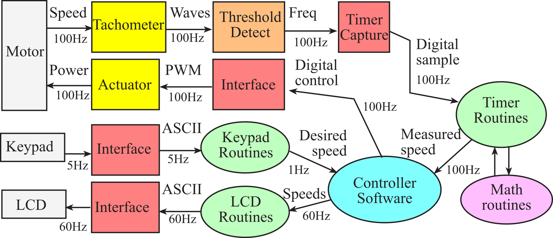
Figure 1.4.2. A data flow graph showing how signals pass through a motor controller.
The next phase is engineering design. We begin by constructing a preliminary design. This system includes the overall top-down hierarchical structure, the basic I/O signals, shared data structures and overall software scheme. At this stage there should be a simple and direct correlation between the hardware/software systems and the conceptual model developed in the high-level design. Next, we finish the top-down hierarchical structure, and build mock-ups of the mechanical parts (connectors, chassis, cables etc.) and user software interface. Sophisticated 3-D CAD systems can create realistic images of our system. Detailed hardware designs must include mechanical drawings. It is a good idea to have a second source, which is an alternative supplier that can sell our parts if the first source can't deliver on time. A call graph is a directed graph showing the calling relationships between software and hardware modules. If a function in module A calls a function in module B, then we draw an arrow from A to B. If a function in module A input/outputs data from hardware module C, then we draw an arrow from A to C. If hardware module C can cause an interrupt, resulting in software running in module A, then we draw an arrow from C to A. A hierarchical system will have a tree-structured call graph.
A call graph for this motor controller is shown in Figure 1.4.3. Again, rectangles represent hardware components and ovals show software modules. An arrow points from the calling routine to the module it calls. The I/O ports are organized into groups and placed at the bottom of the graph. A high-level call graph, like the one shown in Figure 1.4.3, shows only the high-level hardware/software modules. A detailed call graph would include each software function and I/O port. Normally, hardware is passive and the software initiates hardware/software communication, but with interrupts, it is possible for the hardware to interrupt the software and cause certain software modules to be run. In this system, the timer hardware will cause the timer software to collect data from the tachometer. The controller software calls the keypad routines to get the desired speed, calls the timer software to get the motor speed at that point, determines what power to deliver to the motor and updates the actuator by sending the power value to the actuator interface. The controller software calls the LCD routines to display the status of the system. Acquiring data, calculating parameters, outputting results at a regular rate is strategic when performing digital signal processing in embedded systems.
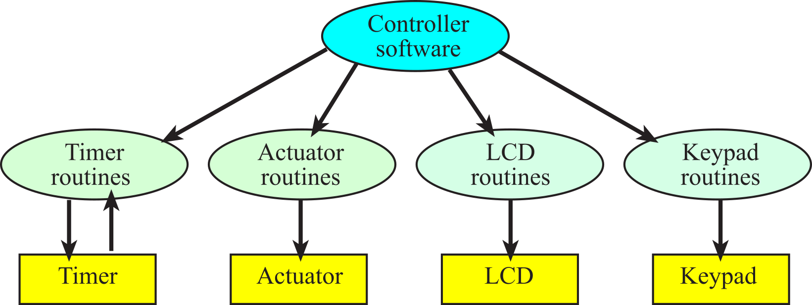
Figure 1.4.3. A call graph for a motor controller.
: What confusion could arise if two software modules were allowed to access the same I/O port? This situation would be evident on a call graph if the two software modules had arrows pointing to the same I/O port.
Observation: If module A calls module B, and B returns data, then a data flow graph will show an arrow from B to A, but a call graph will show an arrow from A to B.
Data structures include both the organization of information and mechanisms to access the data. Again, safety and testing should be addressed during this low-level design.
The next phase is implementation. An advantage of a top-down design is that implementation of subcomponents can occur concurrently. The most common approach to developing software for an embedded system is to use a cross-assembler or cross-compiler to convert source code into the machine code for the target system. The machine code can then be loaded into the target machine. Debugging embedded systems with this simple approach is very difficult for two reasons. First, the embedded system lacks the usual keyboard and display that assist us when we debug regular software. Second, the nature of embedded systems involves the complex and real-time interaction between the hardware and software. These real-time interactions make it impossible to test software with the usual single-stepping and print statements.
The next technological advancement that has greatly affected the way embedded systems are developed is simulation. Because of the high cost and long times required to create hardware prototypes, many preliminary feasibility designs are now performed using hardware/software simulations. A simulator is a software application that models the behavior of the hardware/software system. If both the external hardware and software program are simulated together, even although the simulated time is slower than the clock on the wall, the real-time hardware/software interactions can be studied.
During the initial iterations of the development cycle, it is quite efficient to implement the hardware/software using simulation. One major advantage of simulation is that it is usually quicker to implement an initial product on a simulator versus constructing a physical device out of actual components. Rapid prototyping is important in the early stages of product development. This allows for more loops around the analysis-design-implementation-testing cycle, which in turn leads to a more sophisticated product.
During the testing phase, we evaluate the performance of our system. First, we debug the system and validate basic functions. Next, we use careful measurements to optimize performance such as static efficiency (memory requirements), dynamic efficiency (execution speed), accuracy (difference between expected truth and measured), and stability (consistent operation.) Debugging techniques will be presented throughout the book. Testing is not performed at the end of project when we think we are done. Rather testing must be integrated into all phases of the design cycle. Once tested, the system can be deployed.
Maintenance is the process of correcting mistakes, adding new features, optimizing for execution speed or program size, porting to new computers or operating systems, and reconfiguring the system to solve a similar problem. No system is static. Customers may change or add requirements or constraints. To be profitable, we probably will wish to tailor each system to the individual needs of each customer. Maintenance is not really a separate phase, but rather involves additional loops around the development cycle.
1.4.3. Flowcharts
In this section, we introduce the flowchart syntax that will be used throughout the book. Programs themselves are written in a linear or one-dimensional fashion. In other words, we type one line of software after another in a sequential fashion. Writing programs this way is a natural process, because the computer itself usually executes the program in a top-to-bottom sequential fashion. This one-dimensional format is fine for simple programs, but conditional branching and function calls may create complex behaviors that are not easily observed in a linear fashion. Even the simple systems have multiple software tasks. Furthermore, a complex application will require multiple microcontrollers. Therefore, we need a multi-dimensional way to visualize software behavior. Flowcharts are one way to describe software in a two-dimensional format, specifically providing convenient mechanisms to visualize multi-tasking, branching, and function calls. Flowcharts are very useful in the initial design stage of a software system to define complex algorithms. Furthermore, flowcharts can be used in the final documentation stage of a project to assist in its use or modification.
Figures throughout this section illustrate the syntax used to draw flowcharts. The oval shapes define entry and exit points. The main entry point is the starting point of the software. Each function, or subroutine, also has an entry point, which is the place the function starts. If the function has input parameters, they are passed in at the entry point. The exit point returns the flow of control back to the place from which the function was called. If the function has return parameters, they are returned at the exit point. When the software runs continuously, as is typically the case in an embedded system, there will be no main exit point.
We use rectangles to specify process blocks. In a high-level flowchart, a process block might involve many operations, but in a low-level flowchart, the exact operation is defined in the rectangle. The parallelogram will be used to define an input/output operation. Some flowchart artists use rectangles for both processes and input/output. Since input/output operations are an important part of embedded systems, we will use the parallelogram format, which will make it easier to identify input/output in our flowcharts. The diamond-shaped objects define a branch point or decision block. The rectangle with double lines on the side specifies a call to a predefined function. In this book, functions, subroutines and procedures are terms that all refer to a well-defined section of code that performs a specific operation. Functions usually return a result parameter, while procedures usually do not. Functions and procedures are terms used when describing a high-level language, while subroutines often used when describing assembly language. When a function (or subroutine or procedure) is called, the software execution path jumps to the function, the specific operation is performed, and the execution path returns to the point immediately after the function call. Circles are used as connectors.
Common error: In general, it is bad programming style to develop software that requires a lot of connectors when drawing its flowchart.
Observation: It is good practice to draw flowcharts such that the entire algorithm can be seen on a single page. Sometimes it is better to leave the details out of the flowchart, and into the software itself, so the reader of the flowchart can see the big picture.
There are a seemingly unlimited number of tasks one can perform on a computer, and the key to developing great products is to select the correct ones. Just like hiking through the woods, we need to develop guidelines (like maps and trails) to keep us from getting lost. One of the fundamental issues when developing software, regardless whether it is a microcontroller with 1000 lines of assembly code or a large computer system with billions of lines is to maintain a consistent structure. One such framework is called structured programming. A good high-level language will force the programmer to write structured programs. Structured programs are built from three basic building blocks: the sequence, the conditional, and the while-loop. At the lowest level, the process block contains simple and well-defined commands. I/O functions are also low-level building blocks. Structured programming involves combining existing blocks into more complex structures, as shown in Figure 1.4.4.
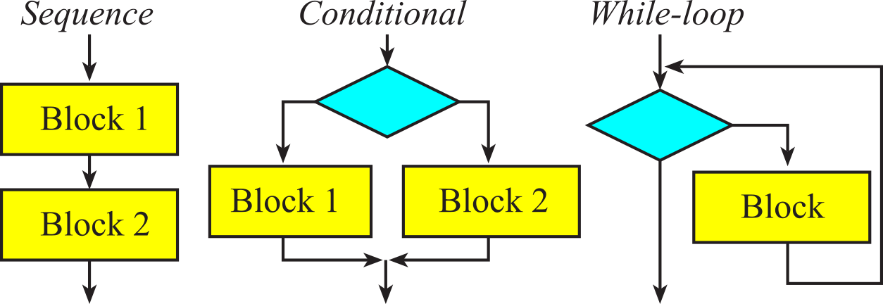
Figure 1.4.4. Flowchart showing the basic building blocks of structured programming.
Maintenance Tip: Remember to update the flowcharts as modifications are made to the software
Next, we will revisit the pacemaker example to illustrate the flowchart syntax. A thread is the sequence of actions caused by executing software. The flowchart in Figure 1.4.5 defines a single-threaded execution because there is one sequence.
Example 1.3.1 (continued): Use a flowchart to describe an algorithm that a pacemaker might use to regulate and improve heart function.
Solution: This example illustrates a common trait of an embedded system, that is, they perform the same set of tasks over and over forever. The program starts at main when power is applied, and the system behaves like a pacemaker until the battery runs out. Figure 1.4.5 shows a flowchart for a very simple algorithm. If the heart is beating normally with a rate greater than or equal to 1 beat/sec (60 BPM), then the atrial sensor will detect activity and the first decision will go right. Since this is normal beating, the ventricular activity will occur within the next 200 ms, and the ventricular sensor will also detect activity. In this situation, no output pulses will be issued. If the delay between atrial contraction and ventricular contract were longer than the normal 200 ms, then the pacemaker will activate the ventricles 200 ms after each atrial contraction. If the ventricle is beating faster than 60 BPM without any atrial contractions, then no ventricular stimulation will be issued. If there is no activity from either atrium or the ventricle (or if that rate is slower than 60 BPM), then the ventricles are paced at 60 BPM.
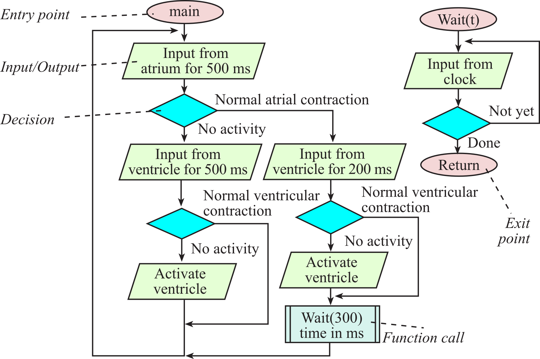
Figure 1.4.5. Flowchart illustrating a simple pacemaker algorithm.
: Assume you are given a simple watch that tells you the current time in hours, minutes, and seconds. Using this watch, define an algorithm to wait time t. The variable t is an input parameter to the algorithm with the same units of hours, minutes, seconds.
1.4.4. Parallel, distributed, and concurrent programming
Many problems cannot be implemented using the single-threaded execution pattern described in the previous section. Parallel programming allows the computer to execute multiple threads at the same time. State-of-the art multi-core processors can execute a separate program in each of its cores. Fork and join are the fundamental building blocks of parallel programming. After a fork, two or more software threads will be run in parallel. I.e., the threads will run simultaneously on separate processors.
Two or more simultaneous software threads can be combined into one using a join. The flowchart symbols for fork and join are shown in Figure 1.4.6. Software execution after the join will wait until all threads above the join are complete. As an analogy, if I want to dig a big hole in my backyard, I will invite three friends over and give everyone a shovel. The fork operation changes the situation from me working alone to four of us ready to dig. The four digging tasks are run in parallel. When the overall task is complete, the join operation causes the friends to go away, and I am working alone again. A complex system may employ multiple microcontrollers, each running its own software. We classify this configuration as parallel or distributed programming.
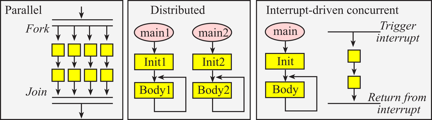
Figure 1.4.6. Flowchart symbols to describe parallel, distributed, and concurrent programming.
Concurrent programming allows the computer to execute multiple threads, but only one at a time. Interrupts are one mechanism to implement concurrency on real-time systems. Interrupts have a hardware trigger and a software action. An interrupt is a parameter-less subroutine call, triggered by a hardware event. The flowchart symbols for interrupts are also shown in Figure 1.4.6. The trigger is a hardware event signaling it is time to do something. Examples of interrupt triggers we will see in this book include new input data has arrived, output device is idle, and periodic event. The second component of an interrupt-driven system is the software action called an interrupt service routine (ISR). The foreground thread is defined as the execution of the main program, and the background threads are executions of the ISRs.
Consider the analogy of sitting in a comfy chair reading a book. Reading a book is like executing the main program in the foreground. Because there is only one of you, this scenario is analogous to a computer with one processor. You start reading at the beginning of the book and basically read one page at a time in a sequential fashion. You might jump to the back and look something up in the glossary, then jump back to where you were, which is analogous to a function call. Similarly, if you might read the same page a few times, which is analogous to a program loop. Even though you skip around a little, the order of pages you read follows a logical and well-defined sequence. Conversely, if the telephone rings, you place a bookmark in the book, and answer the phone. When you are finished with the phone conversation, you hang up the phone and continue reading in the book where you left off. The ringing phone is analogous to hardware trigger and the phone conversation is like executing the ISR.
Notice in this analogy that there is one person who does multiple tasks by doing one task, halting that task, doing a second task to completion, and returning to the original task. In the computer world we have one processor that does one task running the main program, halts that task, does a second task to completion running the ISR, and then returns to the main program.
Example 1.3.2 (continued): Use a flowchart to describe an algorithm that a stand-alone smoke detector might use to warn people in the event of a fire.
Solution: This example illustrates a common trait of a low-power embedded system. The system begins with a power on reset, causing it to start at main. The initialization enables the timer interrupts, and then it shuts off the alarm. In a low-power system the microcontroller goes to sleep when there are no tasks to perform. Every 30 seconds the timer interrupt wakens the microcontroller and executes the interrupt service routine. The first task is to read the smoke sensor. If there is no fire, it will flash the LED and return from interrupt. At this point, the main program will put the microcontroller back to sleep. The letters (A-K) in Figure 1.4.7 specify the software activities in this multithreaded example. Initially it executes A-B-C and goes to sleep. Every 30 seconds, assuming there is no fire, it executes <-D-E-F-G-J-K-J-K-...-J-K-H->C This sequence will execute in about 1 ms, dominated by the time it takes to flash the LED. This is a low-power solution because the microcontroller is powered for about 0.003% of the time, or 1 ms every 30 seconds. We could reduce power even more by sleeping during the 1ms the LED is on.
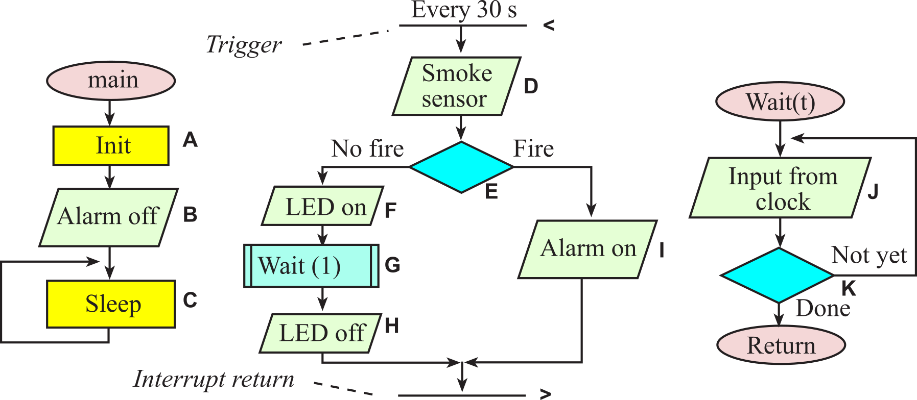
Figure 1.4.7. Flowchart illustrating a simple smoke detector algorithm.
To illustrate the concept of parallel programming, assume we have a multi-core computer with four processors. Consider the problem of finding the maximum value in a large buffer. First, we divide the buffer into four equal parts. Next, we execute a fork, as shown in the left-most flowchart in Figure 1.4.6, launching four parallel threads. The four processors run in parallel each finding the maximum of its subset. When all four threads are complete, they perform a join and combine the four results to find the overall maximum. It is important to distinguish parallel programming like this from multithreading implementing concurrent processing with interrupts. Because most microcontrollers have a single processor, this book with focus on concurrent processing with interrupts and distributed processing with a network involving multiple microcontrollers.
1.4.5. Creative discovery using bottom-up design
Figure 1.4.8 describes top-down design as a cyclic process, beginning with a problem statement and ending up with a solution. With a bottom-up design we begin with solutions and build up to a problem statement. Many innovations begin with an idea, "what if...?" In a bottom-up design, one begins with designing, building, and testing low-level components. Figure 1.4.8 illustrates a two-level process, combining three subcomponents to create the overall product. This hierarchical process could have more levels and/or more components at each level. The low-level designs can occur in parallel. The design of each component is cyclic, iterating through the design-build-test cycle until the performance is acceptable.
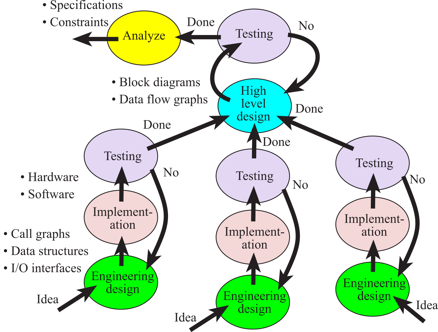
Figure 1.4.8. System development process illustrating bottom-up design.
Bottom-up design is inefficient because some subsystems are designed, built, and tested, but never used. Furthermore, in a truly creative environment most ideas cannot be successfully converted to operational subsystems. Creative laboratories are filled with finished, half-finished, and failed subcomponents. As the design progresses the components are fit together to make the system more and more complex. Only after the system is completely built and tested does one define its overall specifications.
The bottom-up design process allows creative ideas to drive the products a company develops. It also allows one to quickly test the feasibility of an idea. If one fully understands a problem area and the scope of potential solutions, then a top-down design will arrive at an effective solution most quickly. On the other hand, if one doesn't really understand the problem or the scope of its solutions, a bottom-up approach allows one to start off by learning about the problem.
Observation: A good engineer knows both bottom-up and top-down design methods, choosing the approach most appropriate for the situation at hand.
1.5. Fixed and Floating Point Numbers
1.5.1. Fixed-point numbers
We will use fixed-point numbers when we wish to express values in our computer that have noninteger values. A fixed-point number contains two parts. The first part is a variable integer, called I. The second part of a fixed-point number is a fixed constant, called the resolution Δ. The integer may be signed or unsigned. An unsigned fixed-point number is one that has an unsigned variable integer. A signed fixed-point number is one that has a signed variable integer. The precision of a number system is the total number of distinguishable values that can be represented. The precision of a fixed-point number is determined by the number of bits used to store the variable integer. On the ARM, we can use 8, 16 or 32 bits for the integer. Extended precision with more the 32 bits can be implemented, but the execution speed will be slower because the calculations will have to be performed using software algorithms rather than with hardware instructions. This integer part is saved in memory and is manipulated by software. These manipulations include but are not limited to add, subtract, multiply, divide, and square root. The resolution is fixed, and cannot be changed during execution of the program. The resolution is not stored in memory. Usually we specify the value of the resolution using software comments to explain our fixed-point algorithm. The value of the fixed-point number is defined as the product of the variable integer and the fixed constant:
Fixed-point value ≡ I * Δ
Observation: If the range of numbers is known and small, then the numbers can be represented in a fixed-point format.
We specify the range of a fixed-point number system by giving the smallest and largest possible value. The range depends on both the variable integer and the fixed constant. For example, if the system used a 16-bit unsigned variable, then the integer part can vary from 0 to 65535. Therefore, the range of an unsigned 16-bit fixed-point system is 0 to 65535*Δ. In general, the range of the fixed-point system is
Smallest fixed-point value = Imin * Δ, where Imin is the smallest integer value
Largest fixed-point value = Imax * Δ, where Imax is the largest integer value
: What is the range of values for a 16-bit signed fixed-point number with Δ = 0.001?
When interacting with a human operator, it is usually convenient to use decimal fixed-point. With decimal fixed-point the fixed constant is a power of 10.
Decimal fixed-point value ≡ I * 10m for some constant integer m
Again, the m is fixed and is not stored in memory. Decimal fixed-point will be easy to display, while binary fixed-point will be easier to use when performing mathematical calculations. The ARM processor is very efficient performing left and right shifts. With binary fixed-point the fixed constant is a power of 2. An example with a 16-bit integer and Δ=2-6 shown in Figure 1.5.1. Another name for this format is I10.Q6 because there are 10 bits to the left of the binary point and 6 bits to the right.
Binary fixed-point value ≡ I * 2n for some constant integer n
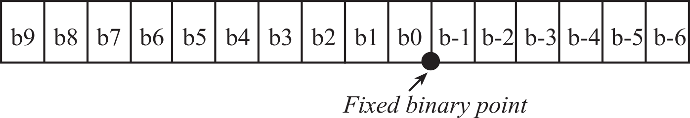
Figure 1.5.1. I10.Q6 16-bit binary fixed-point format with Δ=2-6.
Observation: I10.Q6 does not mean there are two integers, one for I and a second integer for Q. I10.Q6 means there is one 16-bit integer, and Δ=2-6.
: What is the range of values for an unsigned I13.Q3 fixed-point number?
It is good practice to express the fixed-point resolution with units. For example, a decimal fixed-point number with a resolution of 0.001 V is really the same thing as an integer with units of mV. Consider an analog to digital converter (ADC) that converts an analog voltage in the range of 0 to +5 V into a digital number between 0 and 255. This ADC has a precision of 8 bits because it has 256 distinct alternatives. ADC resolution is defined as the smallest difference in input voltage that can be reliably distinguished. Because the 256 alternatives are spread evenly across the 0 to +5V range, we expect the ADC resolution to be about 5V/256 or 0.02V. When we choose a fixed-point number system to represent the voltages we must satisfy two constraints. First, we want the resolution of the number format to be better than the ADC resolution (Δ < 0.02). Second, we want the range of the number system to encompass all the voltages in the range of the ADC (65535*Δ > 5). It would be appropriate to store voltages as 16-bit unsigned decimal fixed-point numbers with a resolution of 0.01V, 0.001V, or 0.0001V.
Using Δ=0.01V, we store 4.23 V by making the integer part equal to 423. If we wished to use binary fixed-point, then we could choose a resolution anywhere in the range of 2-6 to 2-13 V. In general, we want to choose the largest resolution that satisfies both constraints, so the integer parts have smaller values. Smaller numbers are less likely to cause overflow during calculations.
: Give an approximation of π using the decimal fixed-point with Δ = 0.001.
: Give an approximation of π using the binary fixed-point with Δ = 2-8.
Microcontrollers in the TM4C and MPSM0 families provide a 12-bit ADC with a range of 0 to +3.3 V. With a 12-bit ADC, the resolution is 3.3V/4096 or about 0.001V. It would be appropriate to store voltages as 16-bit unsigned fixed-point numbers with a resolution of either 10-3 or 2-10 V. Let Vin be the analog voltage in volts and N be the integer ADC output, then the analog to digital conversion is approximately
N = 4096 * Vin / 3.3
Assume we use a fixed-point resolution of 10-3 V. We use this equation to calculate the integer part of a fixed-point number given the ADC result N. The definition of the fixed-point is
Vin = I * 10-3
Combining the above two equations yields
I = (3300 * N)/ 4096
It is very important to carefully consider the order of operations when performing multiple integer calculations. There are two mistakes that can happen when we calculate 3300*N/4096. The first error is overflow, and it is easy to detect. Overflow occurs when the result of a calculation exceeds the range of the number system. In this example, if the multiply is implemented as 16-bit operation, then 3000*N can overflow the 0 to 65535 range. One solution of the overflow problem is promotion. Promotion is the action of increasing the inputs to a higher precision, performing the calculation at the higher precision, checking for overflow, then demoting the result back to the lower precision. In this example, the 3300, N, and 4096 are all converted to 32-bit unsigned numbers. (3300*N)/4096 is calculated in 32-bit precision. Because we know the range of N is 0 to 4095, we know the calculation of I will yield numbers between 0 and 3300, and therefore it will fit back in a 16-bit variable during demotion. The other error is called drop-out. Drop-out occurs during a right shift or a divide, and the consequence is that an intermediate result loses its ability to represent all of the values. To avoid drop-out, it is very important to divide last when performing multiple integer calculations. If we divided first, e.g., I=3300*(N/4096), then the values of I would always be 0. We could have calculated I=(3300*N+2048)/4096 to implement rounding to the closest integer. The value 2048 is selected because it is about one half of the denominator. Sometimes we can simplify the numbers in an attempt to prevent overflow. In this cause we could have calculated I=(825*N+256)/1024. However, this formulation could still overflow 16-bit math and requires promotion to 32 bits to operate correctly.
When adding or subtracting two fixed-point numbers with the same Δ, we simply add or subtract their integer parts. First, let x, y, and z be three fixed-point numbers with the same Δ. Let x=I*Δ, y=J*Δ, and z=K*Δ. To perform z=x+y, we simply calculate K=I+J. Similarly, to perform z=x-y, we simply calculate K=I-J.
When adding or subtracting fixed-point numbers with different fixed parts, then we must first convert the two inputs to the format of the result before adding or subtracting. This is where binary fixed-point is more efficient, because the conversion process involves shifting rather than multiplication/division. Many instructions on the ARM allow a data shift operation to be performed at no added execution time.
For multiplication, we have z=x*y. Again, we substitute the definitions of each fixed-point parameter and solve for the integer part of the result. If all three variables have the same resolution, then z=x*y becomes K*Δ= I*Δ* J*Δ yielding K = I*J*Δ. If the three variables have different resolutions, such as x=I*2n, y=J*2m, and z=K*2p, then z=x*y becomes K*2p = I*2n * J*2m yielding K = I*J*2n+m-p.
For division, we have z=x/y. Again, we substitute the definitions of each fixed-point parameter and solve for the integer part of the result. If all three variables have the same resolution, then z=x/y becomes K*Δ= (I*Δ)/(J*Δ) yielding K = I/J/Δ. If the three variables have different resolutions, such as x=I*2n, y=J*2m, and z=K*2p, then z=x/y becomes K*2p = (I*2n)/(J*2m) yielding K = (I/J)*2n-m-p. Again, it is very important to carefully consider the order of operations when performing multiple integer calculations. We must worry about overflow and drop-out. If (n-m-p) is positive, then the left shift (I*2n-m-p) should be performed before the divide (/J). Conversely, if (n-m-p) is negative then the right shift should be performed after the divide (/J).
We can approximate a non-integer constant as the quotient of two integers. For example, the difference between 41/29 and √2 is 0.00042. If we need a more accurate representation, we can increase the size of the integers; the difference between 239/169 and √2 is only 1.2E-05. Using a binary fixed-point approximation will be faster on the ARM because of the efficiency of the shift operation. For example, approximating √2 as 181/128 yields an error of 0.0002. Furthermore, approximating √2 as 11585/8192 yields an error of only 2.9E-05.
Observation: For most real numbers in the range of 0.5 to 2, we can find two 3-digit integers I and J such that the difference between the approximation I/J and truth is less than 1E-5. There are 1 million combinations of I and J in the range of 1 to 999. We simply search this space for the best approximation of our real number.
: What is the error in approximating sqrt(5) by 161/72? By 682/305?
We can use fixed-point numbers to perform complex operations using the integer functions of our microcontroller. For example, consider the following digital filter calculation.
y = x -0.0532672*x1 + x2 + 0.0506038*y1-0.9025*y2
In this case, the variables y, y1, y2, x, x1, and x2 are all integers, but the constants will be expressed in binary fixed-point format. The value -0.0532672 will be approximated by -14*2-8. The value 0.0506038 will be approximated by 13*2-8. Lastly, the value -0.9025 will be approximated by -231*2-8. The fixed-point implementation of this digital filter is
y = x + x2 + (-14*x1 + 13*y1 - 231*y2)>>8
Common Error: Lazy or incompetent programmers use floating-point in many situations where fixed-point would be preferable.
Example 1.5.1: Implement a function to calculate the surface area of a cylinder using fixed-point calculations. r is radius of the cylinder, which can vary from 0 to 1 cm. The radius is stored as a fixed-point number with resolution 0.001 cm. The software variable containing the integer part of the radius is n, which can vary from 0 to 1000. The height of the cylinder is 1 cm. The surface area is approximated by
s = 2π * (r2 + r*1cm)
Solution: The surface area can range from 0 to 12.566 cm2 (2π*(12 + 1)). The surface area is stored as a fixed-point number with resolution 0.001 cm2. The software variable containing the integer part of the surface area is m, which can vary from 0 to 12566. In order to better understand the problem, we make a table of expected results.
|
r |
n |
s |
m |
|
0.000 |
0 |
0.000 |
0 |
|
0.001 |
1 |
0.006 |
6 |
|
0.010 |
10 |
0.063 |
63 |
|
0.100 |
100 |
0.691 |
691 |
|
1.000 |
1000 |
12.566 |
12566 |
To solve this problem we use the definition of a fixed-point number. In this case, r is equal to n/1000 and s is equal to m/1000. We substitution these definitions into the desired equation.
s = (6.283)*(r2 + r)
m/1000 = 6.283*((n/1000)2 + (n /1000))
m = 6.283*(n2/1000 + n)
m = 6283*(n2 + 1000*n)/1000000
m = (6283*(n +1000)*n)/1000000
If we wish to round the result to the closest integer we can add ½ the divisor before dividing.
m = (6283*(n +1000)*n+500000)/1000000
One of the problems with this equation is the intermediate result can overflow a 32-bit calculation. One way to remove the overflow is to approximate 2π by 6.28. However, this introduces error. A better way to eliminate overflow is to approximate 2π by 710/113. In fact, 710/113 is a much better approximation of 2π than 6.283 (5.3E-7 versus 1.9E-4).
m = (710*(n +1000)*n+56500)/113000
If we set n to its largest value, n =1000, we calculate the largest value the numerator can be as (710*(1000 +1000)* 1000 +56500) = 1420000355, which fits in a 31-bit number.
Observation: As the fixed constant is made smaller, the accuracy of the fixed-point representation is improved, but the variable integer part also increases. Unfortunately, larger integers will require more bits for storage and calculations.
: Using a fixed constant of 10-3, rewrite the digital filter y = x+0.0532672*x1+x2+0.0506038*y1-0.9025*y2 in decimal fixed-point format.
1.5.2. Floating-point numbers
We can use fixed-point when the range of values is small and known. Therefore, we will not need floating-point operations for most embedded system applications because fixed-point is sufficient. Furthermore, if the processor does not have floating-point instructions then a floating-point implementation will run much slower than the corresponding fixed-point implementation. However, it is appropriate to know the definition of floating-point. NASA believes that there are on the order of 1021 stars in our Universe. Manipulating large numbers like these is not possible using integer or fixed-point formats. Another limitation with integer or fixed-point numbers is there are some situations where the range of values is not known at the time the software is being designed. In a Physics research project, you might be asked to count the rate at which particles strike a sensor. Since the experiment has never been performed before, you do not know in advance whether there will be 1 per second or 1 trillion per second. The applications with numbers of large or unknown range can be solved with floating-point numbers. Floating-point is similar in format to binary fixed-point, except the exponent is allowed to change at run time. Consequently, both the exponent and the mantissa will be stored. Just like with fixed-point numbers we will use binary exponents for internal calculations, and decimal exponents when interfacing with humans. This number system is called floating-point because as the exponent varies the binary point or decimal point moves.
Observation: If the range of numbers is unknown or large, then the numbers must be represented in a floating-point format.
Observation: Floating-point implementations on computers like the Cortex-M0+ that do not have hardware support are extremely long and very slow. So, if you really need floating point, a Cortex-M4F with floating point hardware support is highly desirable.
The IEEE Standard for Binary Floating-Point Arithmetic or ANSI/IEEE Std 754-1985 is the most widely used format for floating-point numbers. The single precision floating point operations on the TM4C microcontrollers are compatible with this standard. There are three common IEEE formats: single-precision (32-bit), double-precision (64-bit), and double-extended precision (80-bits). Only the 32-bit short real format is presented here. The floating-point format, f, for the single-precision data type is shown in Figure 1.5.2. Computers use binary floating-point because it is faster to shift than it is to multiply/divide by 10.
Bit 31 Mantissa sign, s=0 for positive, s=1 for negative
Bits 30:23 8-bit biased binary exponent 0 ≤ e ≤ 255
Bits 22:0 24-bit mantissa, m, expressed as a binary fraction,
A binary 1 as the most significant bit is implied.
m = 1.m1m2m3...m23

Figure 1.5.2. 32-bit single-precision floating-point format.
The value of a single-precision floating-point number is
f = (-1)s * 2e-127* m
The range of values that can be represented in the single-precision format is about ±10-38 to ±10+38. The 24-bit mantissa yields a precision of about 7 decimal digits. The floating-point value is zero if both e and m are zero. Because of the sign bit, there are two zeros, positive and negative, which behave the same during calculations. To illustrate floating-point, we will calculate the single-precision representation of the number 10. To find the binary representation of a floating-point number, first extract the sign.
10 = (-1)0 *10
Step 2, multiply or divide by two until the mantissa is greater than or equal to 1, but less than 2.
10 = (-1)0 *23* 1.25
Step 3, the exponent e is equal to the number of divide by twos plus 127.
10 = (-1)0 *2130-127* 1.25
Step 4, separate the 1 from the mantissa. Recall that the 1 will not be stored.
10 = (-1)0 *2130-127* (1+0.25)
Step 5, express the mantissa as a binary fixed-point number with a fixed constant of 2-23.
10 = (-1)0 *2130-127* (1+2097152*2-23)
Step 6, convert the exponent and mantissa components to hexadecimal.
10 = (-1)0 *2$82-127* (1+$200000*2-23)
Step 7, extract s, e, m terms, convert hexadecimal to binary
10 = (0,$82,$200000) = (0,10000010,01000000000000000000000)
Sometimes this conversion does not yield an exact representation, as in the case of 0.1. In particular, the fixed-point representation of 0.6 is only an approximation.
Step 1 0.1 = (-1)0 *0.1
Step 2 0.1 = (-1)0 *2-4* 1.6
Step 3 0.1 = (-1)0 *2123-127 * 1.6
Step 4 0.1 = (-1)0 *2123-127 * (1+0.6)
Step 5 0.1 ≈ (-1)0 *2123-127* (1+5033165*2-23)
Step 6 0.1 ≈ (-1)0 *2$7B-127* (1+$4CCCCD*2-23)
Step 7 0.1 ≈ (0,$7B,$4CCCCD) = (0,01111011,10011001100110011001101)
The following example shows the steps in finding the floating-point approximation for π.
Step 1 π = (-1)0 * π
Step 2 π ≈ (-1)0 *21* 1.570796327
Step 3 π ≈ (-1)0 *2128-127* 1.570796327
Step 4 π ≈ (-1)0 *2128-127* (1+0.570796327)
Step 5 π ≈ (-1)0 *2128-127* (1+4788187*2-23)
Step 6 π ≈ (-1)0 *2$80-127* (1+$490FDB*2-23)
Step 7 π ≈ (0,$80,$490FDB) = (0,10000000,10010010000111111011011)
There are some special cases for floating-point numbers. When e is 255, the number is considered as plus or minus infinity, which probably resulted from an overflow during calculation. When e is 0, the number is considered as denormalized. The value of the mantissa of a denormalized number is less than 1. A denormalized short result number has the value,
f = (-1)s * 2-126* m where m = 0.m1m2m3...m23
Observation: The floating-point zero is stored in denormalized format.
When two floating-point numbers are added or subtracted, the smaller one is first unnormalized. The mantissa of the smaller number is shifted right and its exponent is incremented until the two numbers have the same exponent. Then, the mantissas are added or subtracted. Lastly, the result is normalized. To illustrate the floating-point addition, consider the case of 10+0.1. First, we show the original numbers in floating-point format. The mantissa is shown in binary format.
10.0 = (-1)0 *23 * 1.01000000000000000000000
+ 0.1 = (-1)0 *2-4* 1.10011001100110011001101
Every time the exponent is incremented the mantissa is shifted to the right. Notice that 7 binary digits are lost. The 0.1 number is unnormalized, but now the two numbers have the same exponent. Often the result of the addition or subtraction will need to be normalized. In this case the sum did not need normalization.
10.0 = (-1)0 *23 * 1.01000000000000000000000
+ 0.1 = (-1)0 *23 * 0.00000011001100110011001 1001101
10.1 = (-1)0 *23 * 1.01000011001100110011001
When two floating-point numbers are multiplied, their mantissas are multiplied and their exponents are added. When dividing two floating-point numbers, their mantissas are divided and their exponents are subtracted. After multiplication and division, the result must be normalized. To illustrate the floating-point multiplication, consider the case of 10*0.1. Let m1, m2 be the values of the two mantissas. Since the range is 1 ≤ m1, m2 < 2, the product m1*m2 will vary from 1 ≤ m1*m2 < 4.
10.0 = (-1)0 *23 * 1.01000000000000000000000
* 0.1 = (-1)0 *2-4 * 1.10011001100110011001101
1.0 = (-1)0 *2-1 *10.00000000000000000000000
The result needs to be normalized.
1.0 = (-1)0 *20 * 1.00000000000000000000000
Roundoff is the error that occurs as a result of an arithmetic operation. For example, the multiplication of two 32-bit mantissas yields a 64-bit product. The final result is normalized into a normalized floating-point number with a 32-bit mantissa. Roundoff is the error caused by discarding the least significant bits of the product. Roundoff during addition and subtraction can occur in two places. First, an error can result when the smaller number is shifted right. Second, when two n-bit numbers are added the result is n+1 bits, so an error can occur as the n+1 sum is squeezed back into an n-bit result.
Truncation is the error that occurs when a number is converted from one format to another. For example, when an 80-bit floating-point number is converted to 32-bit floating-point format, 40 bits are lost as the 64-bit mantissa is truncated to fit into the 24-bit mantissa. Recall, the number 0.1 could not be exactly represented as a short real floating-point number. This is an example of truncation as the true fraction was truncated to fit into the finite number of bits.
If the range is known and small and a fixed-point system can be used, then a 32-bit fixed-point number system will have better resolution than a 32-bit floating-point system. For a fixed range of values (i.e., one with a constant exponent), a 32-bit floating-point system has only 23 bits of precision, while a 32-bit fixed-point system has 9 more bits of precision.
Performance Tip: The single precision floating-point programs written in assembly on the TM4C run much faster than equivalent C code because you can write assembly to perform operations in the native floating point assembly instructions.
1.6. Introduction to Input/Output
1.6.1. General Purpose Input/Output (GPIO)
The simplest I/O port on a microcontroller is the general purpose input/output (GPIO) or parallel port. A GPIO port is a simple mechanism that allows the software to interact with external devices. It is called parallel because multiple signals can be accessed all at once. An input port, which allows the software to read external digital signals, is read only. That means a read cycle access from the port address returns the values existing on the inputs at that time. In particular, the tristate driver (triangle shaped circuit in Figure 1.6.1) will drive the input signals onto the data bus during a read cycle from the port address. A write cycle access to an input port usually produces no effect. The digital values existing on the input pins are copied into the microcontroller when the software executes a read from the port address. There are no input-only ports on TM4C microcontrollers. All GPIO signals on the TM4C are 5-V tolerant when configured as inputs except for PD4, PD5, PB0 and PB1, which are limited to 3.6 V. Only PA1 and PA0 on the MSPM0 are 5-V tolerant, all other pins are limited to 3.6 V.
Observation: Many pins on 3.3-V microcontrollers are not 5-V tolerant. Always check the data sheet when interfacing 5V signals.
Figure 1.6.1. A read only input port allows the software to sense external digital signals.
: What happens if the software writes to an input port like Figure 1.6.1?
Common Error: Many program errors can be traced to confusion between I/O ports and regular memory. For example, you cannot write to an input port.
While an input device usually just involves the software reading the port, an output port can participate in both the read and write cycles very much like a regular memory. Figure 1.6.2 describes a readable output port. A write cycle to the port address will affect the values on the output pins. In particular, the microcontroller places information on the data bus and that information is clocked into the D flip flops. Since it is a readable output, a read cycle access from the port address returns the current values existing on the port pins. There are no output-only ports on TM4C microcontrollers.
Figure 1.6.2. A readable output port allows the software to generate external digital signals.
: What happens if the software reads from an output port like Figure 1.6.2?
To make the microcontroller more marketable, most ports can be software-specified to be either inputs or outputs. Microcontrollers use the concept of a direction register to determine whether a pin is an input (direction register bit is 0) or an output (direction register bit is 1), as shown in Figure 1.6.3. We define an initialization ritual as a program executed during start up that initializes hardware and software. If the ritual software makes direction bit zero, the port behaves like a simple input, and if it makes the direction bit one, it becomes a readable output port. Each digital port pin has a direction bit. This means some pins on a port may be inputs while others are outputs. The digital port pins on most microcontrollers are bidirectional, operating similar to Figure 1.6.3.
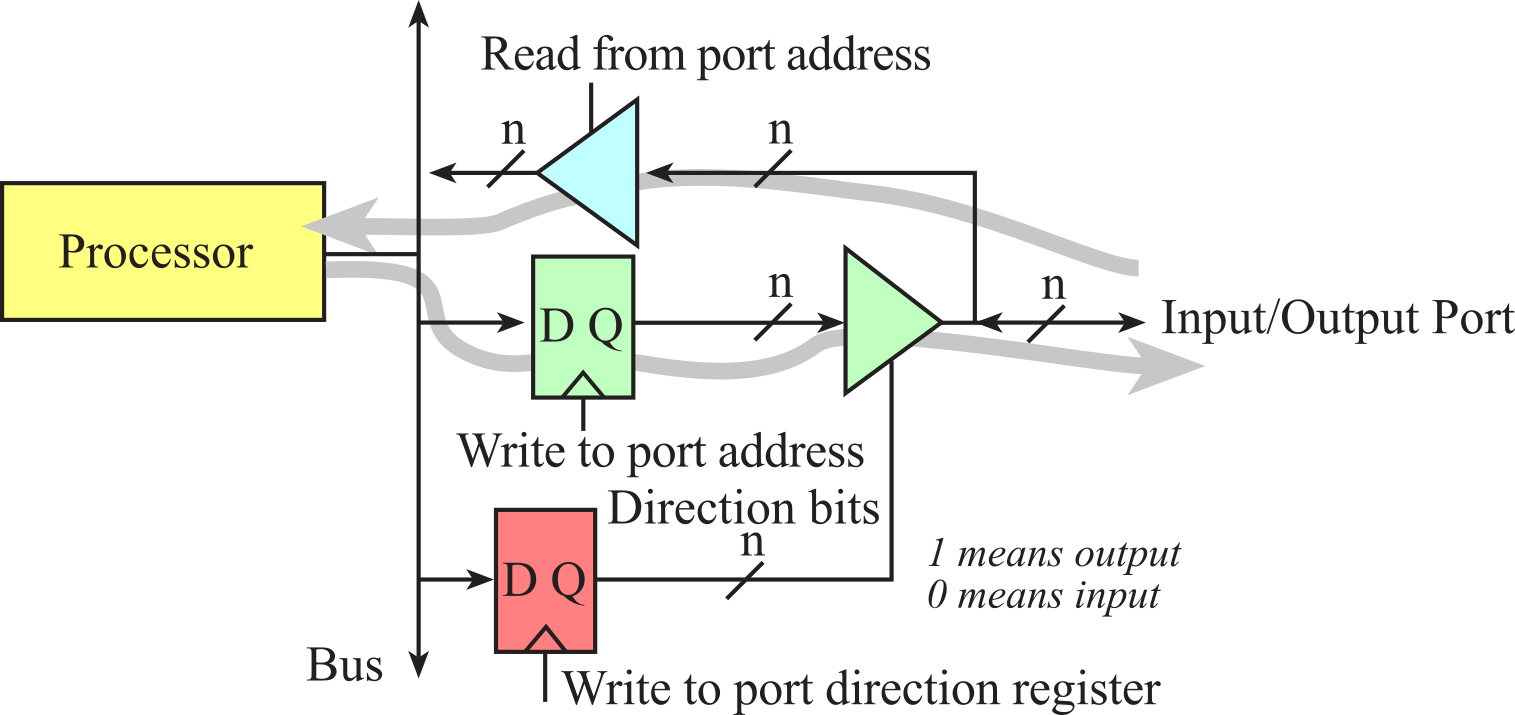
Figure 1.6.3. A bidirectional port can be configured as a read-only input port or a readable output port.
1.6.2. TM4C123 pins
The regular function of a pin is to perform GPIO. Most pins, however, have an alternative function. For a list of alternate functions see Table T.1.3. in the TM4C123 appendix. For example, port pins PA1 and PA0 can be either regular parallel port pins, or an asynchronous serial port called universal asynchronous receiver/transmitter (UART).
Figure 1.6.4 draws the I/O port structure for the TM4C123GH6PM. This microcontroller is used on the EK-TM4C123GXL LaunchPad. Pins on the TM4C family can be assigned to as many as eight different I/O functions. Pins can be configured for digital I/O, analog input, timer I/O, or serial I/O. For example, PD3 can be digital, analog, SSI, I2C, PWM, or timer. There are two buses used for I/O. The digital I/O ports are connected to both the advanced peripheral bus and the advanced high-performance bus. Because of the multiple buses, the microcontroller can simultaneously perform I/O bus cycles with instruction fetches from flash ROM. The TM4C123GH6PM has eight UART ports, four SSI ports, four I2C ports, two 12-bit ADCs, twelve timers, a CAN port, a USB interface, and 16 PWM outputs. There are 43 I/O lines. There are twelve ADC inputs; each ADC can convert up to 1 million samples per second. Section T.1 in Appendix TM4C123 presents the details of how to program the GPIO functionality.
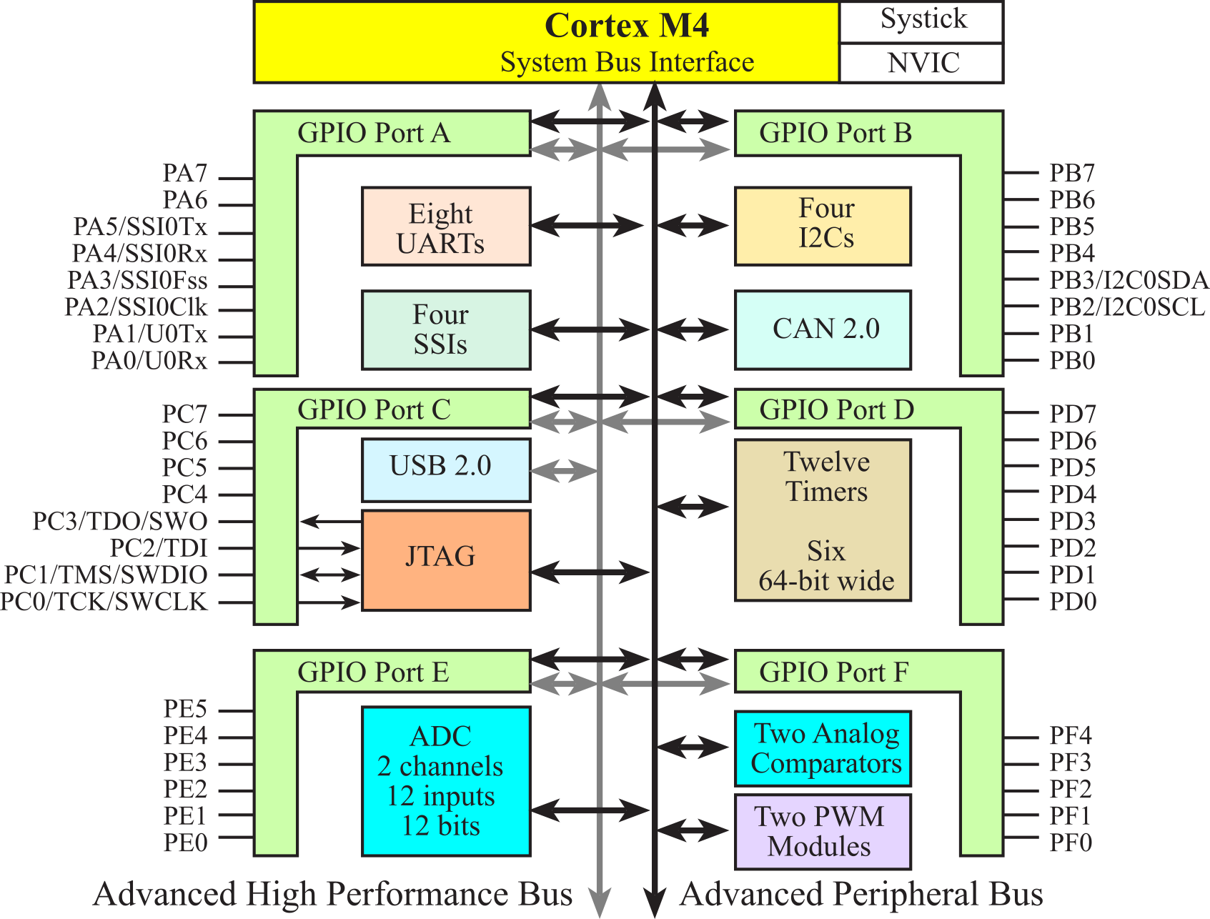
Figure 1.6.4. I/O port pins for the TM4C123GH6PM microcontroller. The TM4C123 USB supports device, host, and on-the-go (OTG) modes.
Joint Test Action Group (JTAG), standardized as the IEEE 1149.1, is a standard test access port used to
program and debug the microcontroller board. The TM4C123 uses Port C, pins
PC3-PC0 for its JTAG interface. Even though it is possible to use PC3-PC0 as
general I/O, debugging most microcontroller boards will be more stable if these
pins are left dedicated to the JTAG debugger. The following lists I/O devices
found on microcontrollers.
- UART Universal asynchronous receiver/transmitter
- SSI Synchronous serial interface
- I2C Inter-integrated circuit
- I2S Inter-IC Sound, Integrated Interchip Sound (not on TM4C)
- Timer Periodic interrupts, input capture, and output compare
- PWM Pulse width modulation
- ADC Analog to digital converter, measurement analog signals
- Comparator Comparing two analog signals
- QEI Quadrature encoder interface
- USB Universal serial bus
- Ethernet High speed network (TM4C1294/MSP432E401Y)
- CAN Controller area network
The UART can be used for serial communication between computers. It is asynchronous and allows for simultaneous communication in both directions. In this book we will use a UART channel to connect to wifi-enabled devices. The SSI is alternately called serial peripheral interface (SPI). It is used to interface medium-speed I/O devices. In this book, we will use it to interface a graphics display, a secure digital card (SDC), and a digital to analog converter (DAC). I2C is a simple I/O bus that we will use to interface low speed peripheral devices. The inter-IC sound, or integrated inter-chip sound I2S protocol is used to communicate sound information between audio devices. Input capture and output compare will be used to create periodic interrupts, and take measurements period, pulse width, phase and frequency. PWM outputs will be used to apply variable power to motor interfaces. In a typical motor controller, input capture measures rotational speed and PWM controls power. A PWM output can also be used to create a DAC. The ADC will be used to measure the amplitude of analog signals and will be important in data acquisition systems. The analog comparator takes two analog inputs and produces a digital output depending on which analog input is greater. The QEI can be used to interface a brushless DC motor. USB is a high-speed serial communication channel. The Ethernet port can be used to bridge the microcontroller to the Internet or a local area network. The CAN creates a high-speed communication channel between microcontrollers and is commonly found in automotive and other distributed control applications.
: Give an example of using time as an input.
: Give an example of using time as an output.
1.6.3. EK-TM4C123GXL LaunchPad
The Texas Instruments LaunchPad evaluation board (Figure 1.6.5) is a low-cost development board available as part number EK-TM4C123GXL from www.ti.com and from regular electronic distributors like Digikey, Mouser, Newark, Arrow, and Avnet. The kit provides an integrated In-Circuit Debug Interface (ICDI), which allows programming and debugging of the onboard TM4C123 microcontroller. One USB cable is used by the debugger (ICDI), and the other USB allows the user to develop USB applications (device). The user can select board power to come from either the debugger (ICDI) or the USB device (device) by setting the Power selection switch.
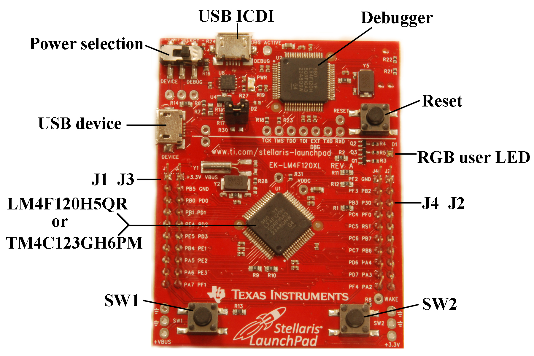
Figure 1.6.5. Texas Instruments LaunchPad based on the TM4C123GH6PM.
The Texas Instruments LaunchPad evaluation board has two switches and one 3-color LED, as shown in Figure 1.6.6. The switches are negative logic and will require activation of the internal pull-up resistors. You will set bits 0 and 4 in GPIO_PORTF_PUR_R register. The LED interfaces on PF3 - PF1 are positive logic. To use the LED, make the PF3 - PF1 pins an output. To activate the red color, output a one to PF1. The blue color is on PF2, and the green color is controlled by PF3. The 0-Ω resistors (R1, R2, R11, R12, R13, R25, and R29) connect the corresponding pin to hardware circuits on the LaunchPad board. LaunchPads come with R25 and R29 removed.
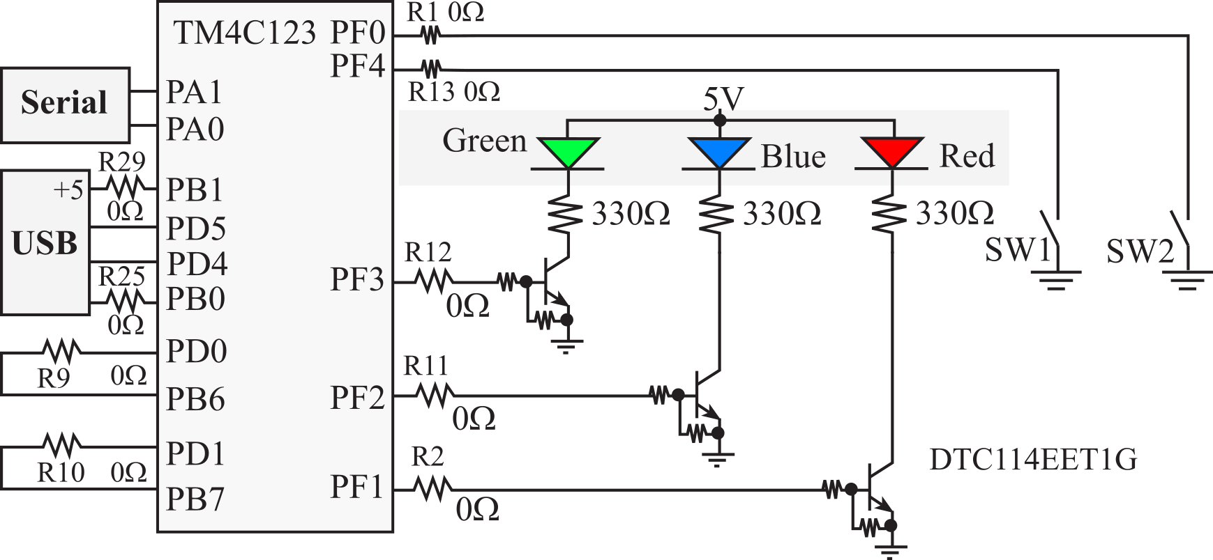
Figure 1.6.6. Switch and LED interfaces on the Texas Instruments LaunchPad Evaluation Board. The zero ohm resistors can be removed so the corresponding pin can be used without connection to the external circuits. We suggest you remove R9 and R10.
The LaunchPad has four 10-pin connectors, labeled as J1 J2 J3 J4 in Figure 1.6.7, to which you can attach your external signals. The top side of these connectors has male pins and the bottom side has female sockets. There are two methods to connect external circuits to the LaunchPad. One method is to purchase a male to female jumper cable (e.g., item number 826 at www.adafruit.com. A second method is to use solid 22-gauge or 24-gauge wire and connect one end of the solid wire into the bottom or female side of the LaunchPad and the other end connects to a solderless breadboard.
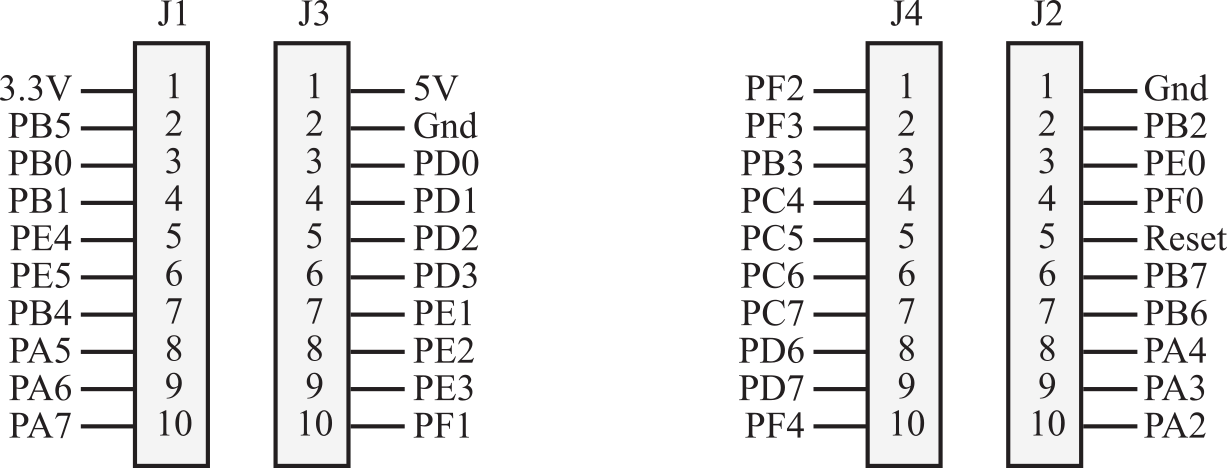
Figure 1.6.7. Interface connectors on the Texas Instruments TM4C123 LaunchPad Evaluation Board.
Pins PA1 - PA0 create a serial port, which is linked through the debugger cable to the PC. The serial link is a physical UART as seen by the TM4C and mapped to a virtual COM port on the PC. The USB device interface uses PD4 and PD5. The JTAG debugger requires pins PC3 - PC0. The LaunchPad connects PB6 to PD0, and PB7 to PD1. If you wish to use both PB6 and PD0 you will need to remove the R9 resistor. Similarly, to use both PB7 and PD1 remove the R10 resistor. The USB connector on the side of the TM4C123 LaunchPad has five wires because it supports device, host, and OTG modes.
Texas Instruments also supplies Booster Packs, which are pre-made external devices that will plug into this 40-pin connector, see Figure 1.6.8.
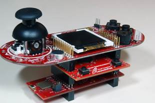
Figure 1.6.8. The MKII educational booster packet provides many input/output devices and the CC2650 booster pack provides Bluetooth low energy (BLE) functionality.
1.6.4. MSPM0G3507 pins
See Volume 1 Section 2.1. MSPM0 I/O Ports
1.6.5. LP-MSPM0G3507 LaunchPad
See Volume 1 Section 2.2. MSPM0G3507 LaunchPad
1.7. Digital Logic
Before we connect external devices to the microcontroller, we must appreciate that digital input/output essentially creates an analog circuit, meaning voltage, current and capacitance are important factors to consider. Digital logic has two states, with many enumerations such as high and low, 1 and 0, true and false, on and off. There are four currents of interest, as shown in Figure 1.7.1, when analyzing if the inputs of the next stage are loading the output. IIH and IIL are the currents required of an input when high and low respectively. Furthermore, IOH and IOL are the maximum currents available at the output when high and low. For the output to properly drive all the inputs of the next stage, the maximum available output current must be larger than the sum of all the required input currents for both the high and low conditions.
![]() and
and
![]()
Absolute value operators are put in the above relations because data sheets are inconsistent about specifying positive and negative currents. The arrows in Figure 1.7.1 define the direction of current regardless of whether the data sheet defines it as a positive or negative current. It is your responsibility to choose parts such that the above inequalities hold.
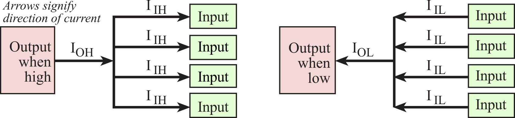
Figure 1.7.1. Sometimes one output must drive multiple inputs.
Kirchhoff's Current Law (KCL) states the sum of all the currents into one node must be zero. The above inequalities are not a violation of KCL, because the output currents are the available currents and the input currents are the required currents. Once the system is built and running, the actual output current will of course exactly equal the sum of the actual input currents. As a matter of completeness, we include Kirchhoff's Voltage Law (KVL), which states the sum of all the voltages in a closed loop must be zero. Table 1.7.1 shows typical current values for the various digital logic families. The TM4C123 microcontrollers give you three choices of output current for the digital output pins. The MSPM0G3507 has four pins that can drive 20mA, and the rest of the pins can drive 6mA.
|
Family |
Example |
IOH |
IOL |
IIH |
IIL |
|
Standard TTL |
7404 |
0.4 mA |
16 mA |
40 µA |
1.6 mA |
|
Schottky TTL |
74S04 |
1 mA |
20 mA |
50 µA |
2 mA |
|
Low Power Schottky |
74LS04 |
0.4 mA |
4 mA |
20 µA |
0.4 mA |
|
High Speed CMOS |
74HC04 |
4 mA |
4 mA |
1 µA |
1 µA |
|
Adv Hi Speed CMOS |
74AHC04 |
4 mA |
4 mA |
1 µA |
1 µA |
|
TM4C 2mA-drive |
TM4C123 |
2 mA |
2 mA |
2 µA |
2 µA |
|
TM4C 4mA-drive |
TM4C123 |
4 mA |
4 mA |
2 µA |
2 µA |
|
TM4C 8mA-drive |
TM4C123 |
8 mA |
8 mA |
2 µA |
2 µA |
|
MSPM0 |
MSPM0G3507 |
6 mA |
6 mA |
50 nA |
50 nA |
|
MSPM0 Hi-drive |
PA31,28,11,10 |
20 mA |
20 mA |
50 nA |
50 nA |
Table 1.7.1. The input and output currents of various digital logic families and microcontrollers.
Observation: For TTL devices the logic low currents are much larger than the logic high currents.
When we design circuits using devices all from a single logic family, we can define fan out as the maximum number of inputs, one output can drive. For transistor-transistor logic (TTL) logic we can calculate fan out from the input and output currents:
Fan out = minimum( (IOH/IIH) , (IOL/IIL) )
Conversely, the fan out of high-speed complementary metal-oxide semiconductor (CMOS) devices, which includes most microcontrollers, is determined by capacitive loading and not by the currents. Figure 1.7.2 shows a simple circuit model of a CMOS interface. The ideal voltage of the output device is labeled V1. For interfaces in close proximity, the resistance R results from the output impedance of the output device, and the capacitance C results from the input capacitance of the input device. However, if the interface requires a cable to connect the two devices, both the resistance and capacitance will be increased by the cable. The voltage labeled V2 is the effective voltage as seen by the input. If V2 is below 1.3 V, the TM4C microcontrollers will interpret the signal as low. Conversely, the voltage is above 2.0 V, these microcontrollers will consider it high. The slew rate of a signal is the slope of the voltage versus time during the time when the logic level switches between low and high. A similar parameter is the transition time, which is the time it takes for an output to switch from one logic level to another. In Figure 1.7.2, the transition time is defined as the time it takes V2 to go from 1.3 to 2.0 V. There is a capacitive load for the output and each input. As this capacitance increases the slew rate decreases, which will increase the transition time. Signals with a high slew rate can radiate a lot of noise. So, to reduce noise emissions we sometimes limit the slew rate of the signals.
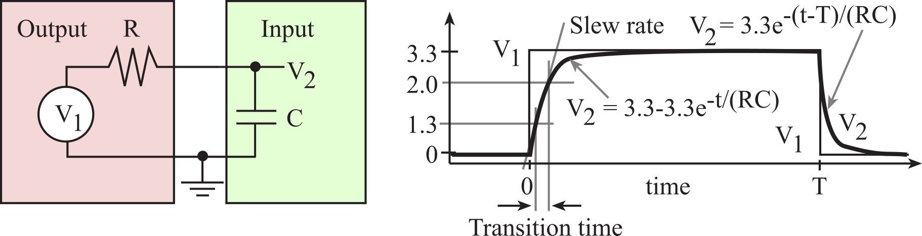
Figure 1.7.2. Capacitance loading is an important factor when interfacing CMOS devices.
Observation: The understanding of Figure 1.7.2 is a common interview question when looking for an embedded systems position.
There are two ways to determine the fan out of CMOS circuits. First, some circuits have a minimum time its input can exist in the transition range. For example, it might specify the signal cannot be above 1.3 and below 2.0 V for more than 20 ns. Clock inputs are often specified this way. A second way is to calculate the time constant τ, which is R*C for this circuit. Let T be the pulse width of the digital signal. If T is large compared to τ, then the CMOS interface functions properly. For circuits that mix devices from one family with another, we must look individually at the input and output currents, voltages and capacitive loads. There is no simple formula.
Figure 1.7.3 compares the input and output voltages for many of the digital logic families. VIL is the voltage below which an input is considered a logic low. Similarly, VIH is the voltage above which an input is considered a logic high. The output voltage depends strongly on current required to drive the inputs of the next stage. VOH is the output voltage when the signal is high. In particular, if the output is a logic high, and the current is less than IOH, then the voltage will be greater than VOH. Similarly, VOL is the output voltage when the signal is low. In particular, if the output is a logic low, and the current is less than IOL, then the voltage will be less than VOL. Most digital input pins on the TM4C microcontrollers are 5V-tolerant, meaning an input high signal can be any voltage from 2.145 to 5.0 V. PD4, PD5, PB0 and PB1 are limited to 3.6 V. Only PA1 and PA0 on the MSPM0 are 5-V tolerant, all other pins are limited to 3.6 V.
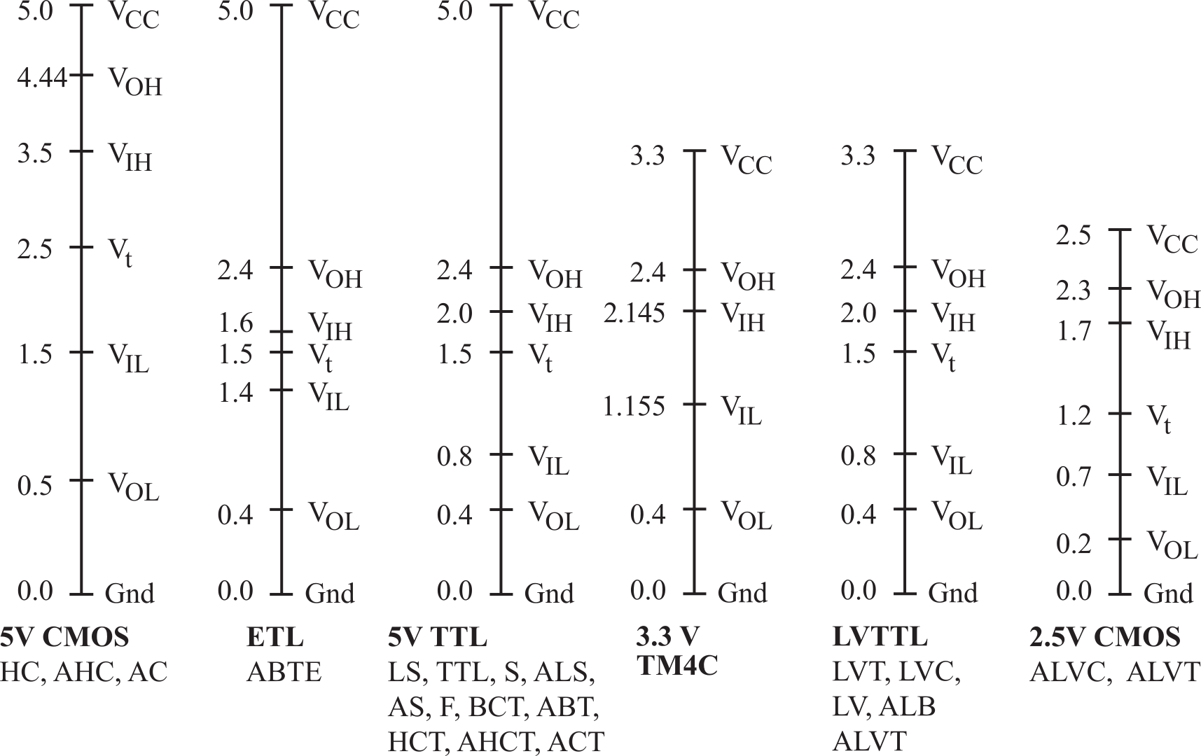
Figure 1.7.3. Voltage thresholds for various digital logic families.
Observation: Noise margin is the minimum of VIL - VOL and VOH - VIH.
: What is the noise margin on a TM4C123? What is the noise margin on an MSPM0G3507?
For the output of one circuit to properly drive the inputs
of the next circuit, the output low voltage needs to be low enough, and the
output high voltage needs to be high enough.
VOL ≤ VIL for all inputs and
VOH ≥ VIH for all inputs
The maximum output current specification on the TM4C
family is 25 mA, which is the current above which will cause damage. However,
we can select IOH and IOL to be 2, 4, or 8
mA.
The data sheet for the MSPM0 recommends limiting the current on standard output pins
to 6mA max, and 20mA max for high-drive pins.
It is good practice to design the system so the output currents are less than IOH
and IOL. Vt is the typical threshold
voltage, which is the voltage at which the input usually switches between logic
low and high. Formally however, an input is considered in the transition region
for voltages between VIL and VIH. Noise
margin is how much added noise can the signal take and still operate. The
five parameters that affect our choice of logic families are
- Power supply voltage (e.g., +5V, 3.3V etc.)
- Power supply current (e.g., will the system need to run on batteries?)
- Speed (e.g., clock frequency and propagation delays)
- Output drive, IOL, IOH (e.g., does it need to drive motors or lights?)
- Noise margin (e.g., VIL-VOLand VOH-VIH)
- Temperature sensitivity and electromagnetic field interference)
: How will the TM4C123 interpret an input pin as the input voltage changes from 0, 1, 2, 3, 4, to 5V? I.e., for each voltage, will it be considered as a logic low, as a logic high or as indeterminate?
: Considering both voltage and current, can the output of a 74HC04 drive the input of a 74LS04? Assume both are running at 5V.
: Considering both voltage and current, can the output of a 74LS04 drive the input of a 74HC04? Assume both are running at 5V.
A very important concept used in computer technology is tristate logic, which has three output states: high, low, and off. Other names for the off state are HiZ, floating, and tristate. Tristate logic is drawn as a triangle shape with a signal on the top of the triangle. In this Figure 1.7.4, A is the data input, G is the gate input, and B is the data output. When there is no circle on the gate, it operates in positive logic, meaning if the gate is high, then the output data equals the input data. If the positive-logic gate is low, then the output will float. When there is a circle on the gate, it operates in negative logic, meaning if the gate is low, then the output data equals the input data. If the negative-logic gate is high, then the output will float.
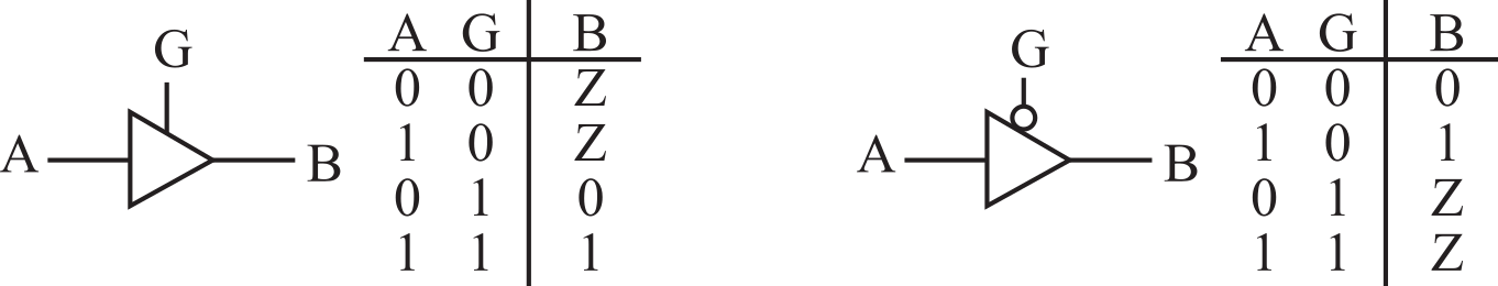
Figure 1.7.4. Digital logic drawing of tristate drivers.
The 74LS04 is a low-power Schottky NOT gate, as shown on the left in Figure 1.7.5. It is called Schottky logic because the devices are made from Schottky transistors. The output is high when the transistor Q4 is active, driving the output to Vcc. The output is low when the transistor Q5 is active, driving the output to 0.
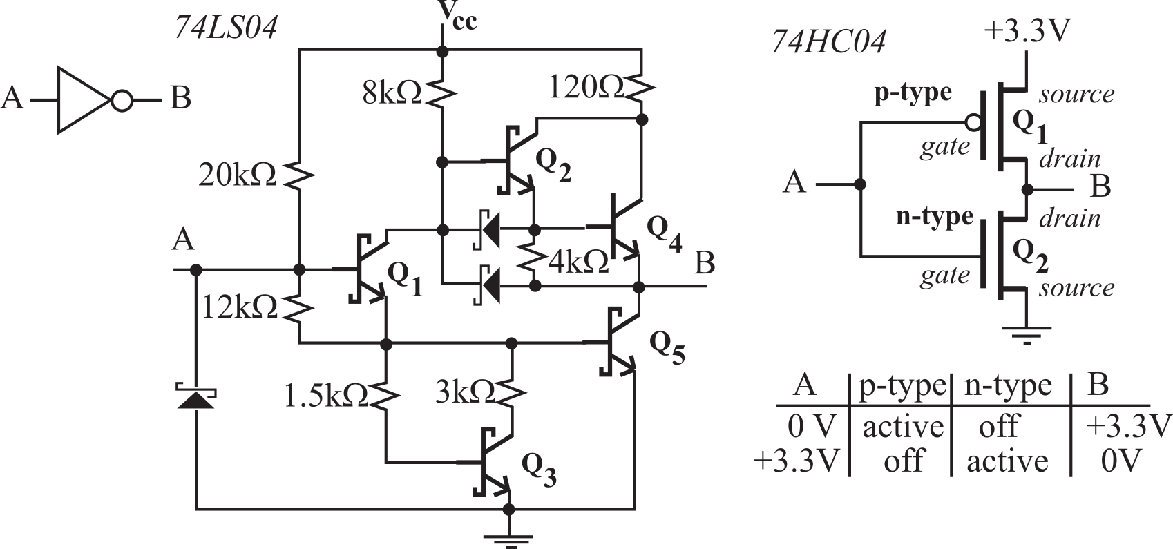
Figure 1.7.5. Two transistor-level implementations of a NOT gate.
It is obviously necessary to read the data sheet for your microcontroller. However, it is also good practice to review the errata published by the manufacturer about your microcontroller. The errata define situations where the actual chip does not follow specifications in the data sheet. Most of TM4C123 input pins are +5V tolerant. However, PD4, PD5, PB0 and PB1 are limited to 3.6 V.
The 74HC04 is a high-speed CMOS NOT gate, shown on the right in Figure 1.7.5. The output is high when the transistor Q1 is active, driving the output to 3.3V. The output is low when the transistor Q2 is active, driving the output to 0. Since most microcontrollers are made with high-speed CMOS logic, its outputs behave like the Q1/Q2 "push/pull" transistor pair. Output ports are not inverting. I.e., when you write a "1" to an output port, then the output voltage goes high. Similarly, when you write a "0" to an output port, then the output voltage goes low. Analyses of the circuit in Figure 1.7.5 reveal some of the basic properties of high-speed CMOS logic. First, because of the complementary nature of the P-channel (the one on the top) and N-channel (the one on the bottom) transistors, when the input is constant (continuously high or continuously low), the supply current, Icc, is very low. Second, the gate will require supply current only when the output switches from low to high or from high to low. This observation leads to the design rule that the power required to run a high-speed CMOS system is linearly related to the frequency of its clock, because the frequency of the clock determines the number of transitions per second. Along the same lines, we see that if the voltage on input A exists between VIL and VIH for extended periods of time, then both Q1 and Q2 are partially active, causing a short from power to ground. This condition can cause permanent damage to the transistors. Third, since the input A is connected to the gate of the two MOS transistors, the input currents will be very small (≈1 µA). In other words, the input impedance (input voltage divide by input current) of the gate is very high. Normally, a high input impedance is a good thing, except if the input is not connected. If the input is not connected then it takes very little input currents to cause the logic level to switch.
Common error: If unused input pins on a CMOS microcontroller are left unconnected, then the input signal may oscillate at high frequencies depending on the EM fields in the environment, wasting power unnecessarily.
Observation: It is a good design practice to connect unused CMOS inputs to ground or connect them to +3.3V.
Now that we understand that CMOS digital logic is built with PNP and NPN transistors, we can revisit the interface requirements for connecting a digital output from one module to a digital input of another module. Figure 1.7.6 shows the model when the output is high. To make the output high, a PNP transistor in the output module is conducting (Q1) driving +3.3 V to the output. The high voltage will activate the gate of NPN transistors in the input module (Q4). The IIH is the current into the input module needed to activate all gates connected to the input. The actual current I will be between 0 and IIH. For a high signal, current flows from +3.3V, across the source-drain of Q1, into the gate of Q4, and then to ground. As the actual current I increases, the actual output voltage V will drop. IOH is the maximum output current that guarantees the output voltage will be above VOH. Assuming the actual I is less than IOH, the actual voltage V will be between VOH and +3.3V. If the input voltage is between VIH and +3.3V, the input signal is considered high by the input. For the high signal to be transferred properly, VOH must be larger than VIH and IOH must be larger than IIH.
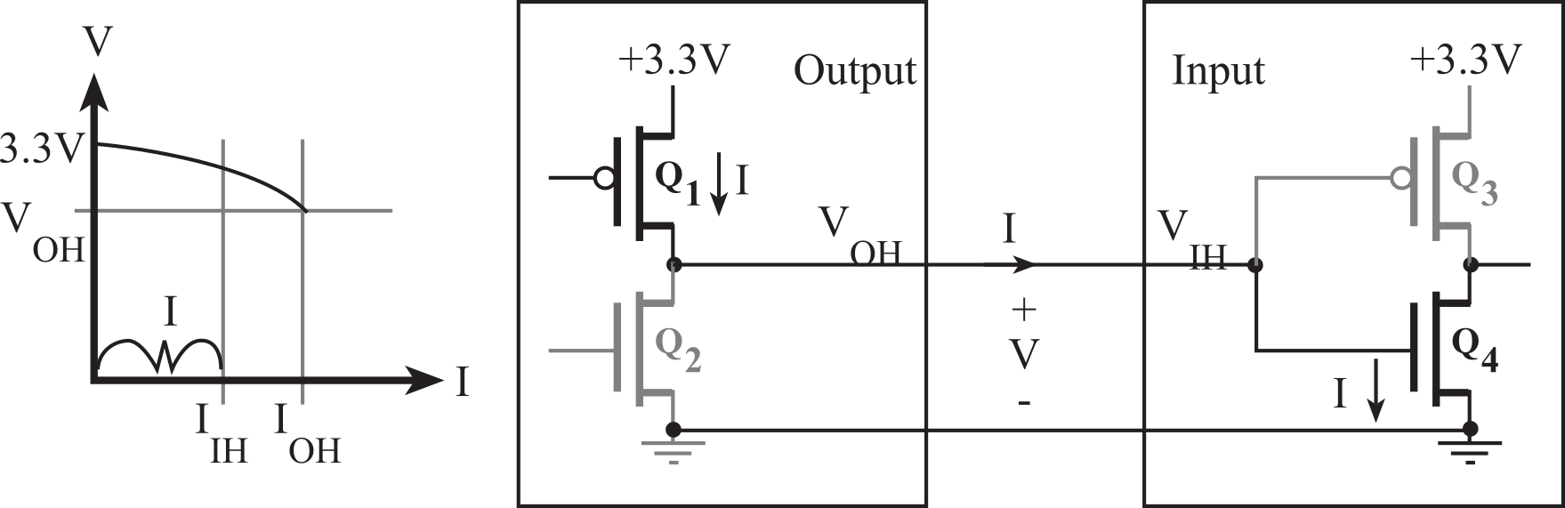
Figure 1.7.6. Model for the input/output characteristics when the output is high.
Figure 1.7.7 shows the model when the output is low. To make the output low, an NPN transistor in the output module is conducting (Q2) driving the output to 0V. The low voltage will activate the gate of PNP transistors in the input module (Q3). The IIL is the current out of the input module needed to activate all gates connected to the input. The actual current I will be between 0 and IIL. For a low signal, current flows from +3.3V in the input module, across the source-gate of Q3, across the source-drain gate of Q2, and then to ground. As the actual current I increases, the actual output voltage V will increase. IOL is the maximum output current that guarantees the output voltage will be less than VOL. Assuming the actual I is less than IOL, the actual voltage V will be between 0 and VOL. If the input voltage is between 0 and VIL, the input signal is considered low by the input. For the low signal to be transferred properly, VOL must be less than VIL and IOL must be larger than IIL.
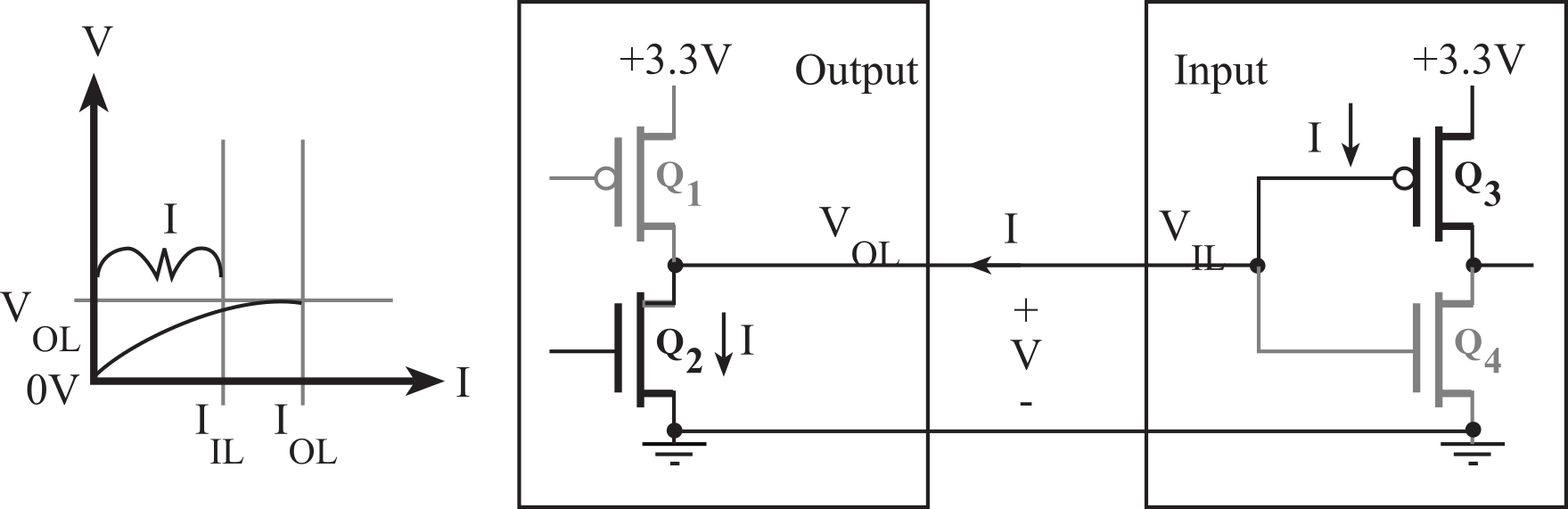
Figure 1.7.7. Model for the input/output characteristics when the output is low.
Open collector logic has outputs with two states: low and off. The 74LS05 is a low-power Schottky open collector NOT gate, as shown in Figure 1.7.8. When drawing logic diagrams, we add the 'x' on the output to specify open collector logic.
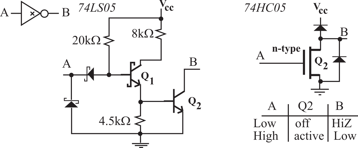
Figure 1.7.8. Two transistor implementations of an open collector NOT gate. The 74HC05 is open drain.
The 74HC05 is a high-speed CMOS open collector NOT gate is also shown in Figure 1.7.8. It is called open collector because the collector pin of Q2 is not connected, or left open. The output is off when there is no active transistor driving the output. In other words, when the input is low, the output floats. This "not driven" condition is called the open collector state. When the input is high, the output will be low, caused by making the transistor Q2 is active driving the output to 0. Technically, the 74HC05 implements open drain rather than open collector, because it is the drain pin of Q2 that is left open. In this book, we will use the terms open collector and open drain interchangeably to refer to digital logic with two output states (low and off). Because of the multiple uses of open collector, many microcontrollers can implement open collector logic. On TM4C microcontrollers, we can affect this mode by defining an output as open drain.
1.8. Switch and LED Interfaces
1.8.1 Switch Interfaces
We begin input/output by connecting switches to the microcontroller. Figure 1.8.1 shows a mechanical switch with one terminal connected to ground. In this circuit, when the switch is pressed, the voltage y is zero. When the switch is not pressed, the signal y floats. We use a pull-up resistor to create a digital logic signal, s, which we will connect to an input pin of the microcontroller.
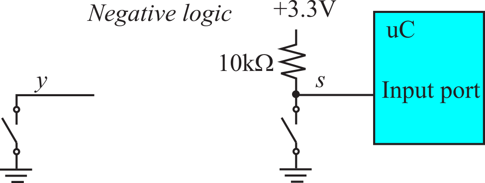
Figure 1.8.1. Negative logic Single Pole Single Throw (SPST) Switch interface.
We encourage you to read the data sheet for your switch and find which pins connect to the switch. Data sheet for the B3F-1059
Video 1.8.1. B3F Switch Datasheet
How do we select the value of the resistor? In general, the smaller the resistor, the larger the current it will be able to supply when the switch is open. On the other hand, a larger resistor does not waste as much current when the switch is closed. One way to calculate the value of this pull-up resistor is to first determine the required output high voltage, Vout, and output high current, Iout. When connecting to the microcontroller, we need Iout of the switch to be larger than IIH. VIH is 2.145V, but to be on the save side, we make Vout greater than 3.2 V. To supply a current of at least Iout at a voltage above Vout, the resistor must be less than:
R ≤ (VCC - Vout)/Iout
R ≤ (3.3V-3.2V)/2µA = 50kΩ
When the switch in Figure 1.8.1 is pressed the voltage at s still goes to zero, because the resistance of the switch (less than 0.1Ω) is much less than the 10kΩ pull-up resistor. But now when the switch is not pressed, the pull-up resistor creates a logic high at s. This circuit is shown connected to an input pin of the microcontroller. The software, by reading the input port, can determine whether the switch is pressed. If the switch is pressed the software will read zero, and if the switch is not pressed the software will read one. Figure 1.8.1 is called negative logic because the active state, switch being pressed, has a lower voltage than the inactive state.
Another switch interface is shown in Figure 1.8.2. When the switch is pressed, the voltage x is 3.3V. When the switch is not pressed, the signal x floats. We use a pull-down resistor to create a digital logic signal, t, which we will connect to an input pin of the microcontroller. This circuit is called positive logic because the active state, switch being pressed, has a higher voltage than the inactive state.
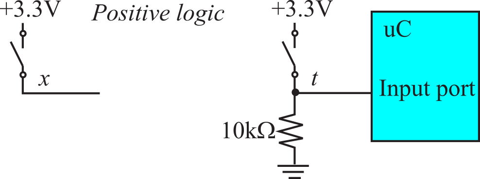
Figure 1.8.2. Positive logic Single Pole Single Throw (SPST) Switch interface.
One way to calculate the value of this down-up resistor is to first determine the required output low voltage, Vout, and output low current, Iout. When connecting to the microcontroller, we need Iout of the switch to be larger than IIL. VIL is 1.155V, but to be on the save side, we make Vout less than 0.1 V. To supply a current of at least Iout at a voltage below Vout, the resistor must be less than:
R ≤ Vout/Iout
R ≤ 0.1V/2µA = 50kΩ
Previously, we used voltage and current arguments to determine the value of the pull-up and pull-down resistors. Consider another method one could use to select these resistors. The TM4C microcontrollers have an input current of 2 µA. At 3.3 V, this is the equivalent of an input impedance of about 1 MΩ (3.3V/2µA). A switch has an on-resistance of less than 0.1 Ω. We want the resistor to be small when compared to 1 MΩ, but large compared to 1 Ω. The 10 kΩ pull-up resistor is 100 times smaller than the input impedance and 100,000 times larger than the switch resistance. For the TM4C, the internal pull-up resistor ranges from 13 to 30 kΩ, and the internal pull-down resistor ranges from 13 to 35 kΩ.
Observation: We can activate pull-up or pull-down resistors on the ports on most microcontrollers, so the interfaces in Figures 1.8.1 and 1.8.2 can be made without the external resistor.
1.8.2 LED Interfaces
A light emitting diode (LED) emits light when an electric current passes through it, see Figure 1.8.3. LEDs have polarity, meaning current must pass from anode to cathode to activate. The anode is labeled a or + , and cathode is labeled k or -. The cathode is the short lead and there may be a slight flat spot on the body of round LEDs. Thus, the anode is the longer lead. The brightness of an LED depends on the applied electrical power (P=I*V).

Figure 1.8.3. LEDs.
Since the LED voltage is approximately constant in the active region (see left side of Figure 1.8.4), we can establish the desired brightness by setting the current by choosing the appropriate resistance value.
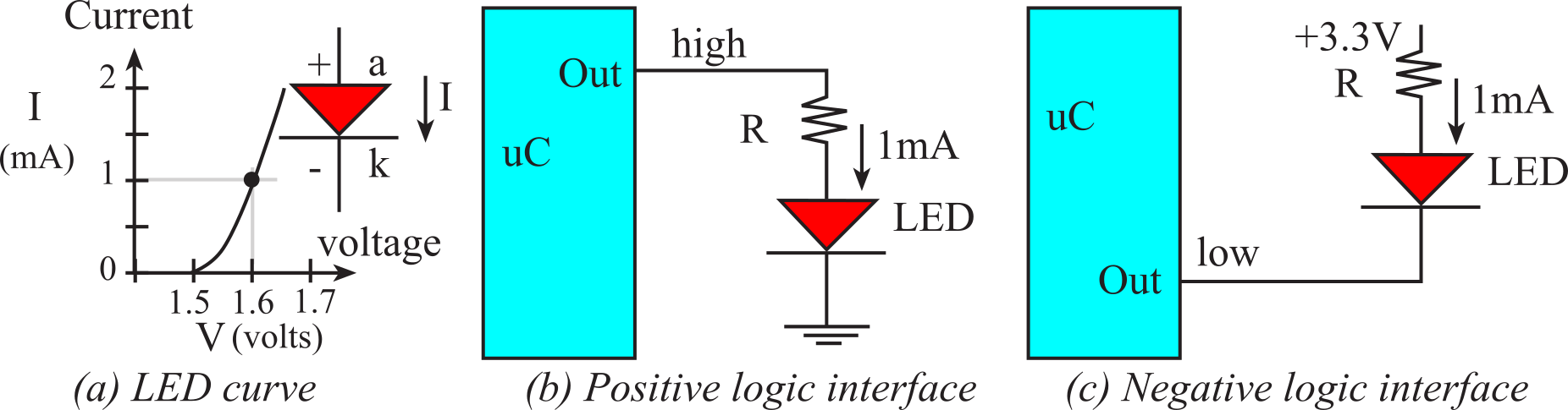
Figure 1.8.4. Low current LED interface (Agilent HLMP-D150).
We encourage you to open up the data sheet for your LED and find the curve similar to Figure 1.8.4. Data sheet for HLMP-4700.
When the LED current is less than 8 mA, we can interface
it directly to an output pin without using a driver. The LED shown in Figure 1.8.4
has an operating point of 1.6 V and 1 mA. For the
positive logic interface, we calculate the resistor value based on the desired
LED voltage and current:
R = (VOH-Vd)/Id
= (2.4-1.6)/(0.001) = 800Ω
where VOH is
the output high voltage of the microcontroller output
pin. Since VOH can vary from 2.4 to 3.3 V, it makes sense to
choose a resistor from a measured value of VOH, rather than
the minimum value of 2.4 V.
Negative logic means the LED is
activated when the software outputs a zero. For the negative logic interface
we use a similar equation to determine the
resistor value
R = (3.3-Vd-VOL)/Id
= (3.3-1.6-0.4)/(0.001) = 1.3kΩ
where VOL is
the output low voltage of the microcontroller output pin.
If we use a 1.2 kΩ in place of the 1.3 kΩ, then the current will be (3.3-1.6-0.4V)/1.2kΩ, which is about 1.08 mA. This slightly higher current is usually acceptable. If we use a standard resistor value of 1.5 kΩ in place of the 1.3 kΩ, then the current will be (3.3-1.6-0.4V)/1.5kΩ, which is about 0.87 mA. This slightly lower current is also usually acceptable.
Observation: Remember to enable the high current drive functionality on the GPIO output pin when interfacing an LED. On the TM4C123, this is the DR8R register. On the MSPM0, this is the DRV bit in the PINCM register, which is available for PA31, PA28, PA11 and PA10.
Design for tolerance means making it work for a range of possibilities. Assume the resistor value in Figure 1.8.4 is 1.3kΩ, and the diode voltage remains at 1.6V. The VOL could range from 0 to 0.4 V. At VOL=0V, Id=(3.3-1.6-0.0V)/1.3kΩ, which is about 1.3 mA. At VOL=0.4V, Id=(3.3-1.6-0.4V)/1.3kΩ, which is about 1.0 mA. So the uncertainty in VOL causes a 1.0 to 1.3 mA uncertainty in Id. This is usually acceptable. However, it makes sense to measure each of these voltages and currents in the actual circuit to verify its proper operation.
: What resistor value in Figure 1.8.4 is needed if the desired LED operating point is 1.8V and 4 mA? Assume VOH is 3.1V. Use the positive logic interface.
: What resistor value in Figure 1.8.4 is needed if the desired LED operating point is 1.7V and 2 mA? Assume VOL is 0.3V. Use the negative logic interface.
Observation: Using standard resistor values will make our product less expensive and easier to obtain parts.
Software to input from PD7 and output to PD3 is presented in Program T.1.1. in the TM4C123 appendix.
If the LED current is above 8 mA, we cannot connect it directly to the microcontroller because the high currents may damage the chip. There are many possible solutions to interface an LED needing more than 8 mA of current. Examples include 7405, 7406 or PN2222. We have chosen the ULN2003B because it has 7 drivers in each package. The ULN2003B comes in a DIP package with 7 base (B) signals, 7 collector (C) signals and one emitter (E) pin. Figure 1.8.5 shows one driver in the ULN2003B.The B signals are the inputs, the C signals are the outputs, and the E pin will be grounded. If the base input is high, the collector output will be low (0.5V). If the base input is low, the collector output will float (neither high nor low).
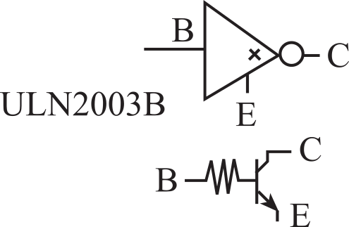
Figure 1.8.5. The ULN2003B LED driver.
For high current LEDs we typically use the 5V supply
rather than the 3.3V, because the available current at 5V is often much
more than the available current at 3.3V. Figure 1.8.6 shows how to
interface a 10 mA 1.9V LED using the ULN2003B. When the software writes a
logic 1 to the output port, the input to the ULN2003B becomes high, output
from the ULN2003B becomes low, 10 mA travels through the LED, and the LED
is on. When the software writes a logic 0 to the output port, the input to
the ULN2003B becomes low, output from the ULN2003B floats (neither high
nor low), no current travels through the LED, and the LED is dark.
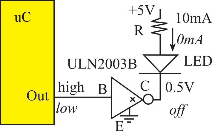
Figure 1.8.6. Interface a high current LED using a ULN2003B driver.
The value of the resistor is selected to establish the proper LED current. When active, the LED voltage will be between 1.8 and 2.2 V, and the power delivered to the LED will be controlled by its current. If the desired brightness requires an operating point of 1.9 V at 10 mA, then the resistor value should be
R = (5 - Vd - VCE) / Id = (5 - 1.9- 0.5) /0.01 = 260Ω
where Vd, Id is the desired LED operating point, and VCE is the output low voltage of the LED driver. If we use a standard resistor value of 270Ω in place of the 260Ω, then the current will be (5-1.9-0.5V)/270Ω, which is about 9.6 mA. This slightly lower current is usually acceptable.
: What resistor value in Figure 1.8.6 is needed if the desired LED operating point is Vd=1.7V and Id=11 mA?
1.9. SysTick Periodic Interrupts
We will use interrupts extensively in this class. However, this class has Introduction to Embedded Systems (ECE319K) as a prerequisite. The prerequisite material for this section can be found in Sections 6.1 through 6.5 in the ECE319K ebook. Please review this material before reading this section.
Table 1.9.1 shows the SysTick registers used to create a periodic interrupt. SysTick has a 24-bit counter that decrements at the bus clock frequency. Let fBUS be the frequency of the bus clock, and let n be the value of the RELOAD register. The frequency of the periodic interrupt will be fBUS/(n+1). First, we clear the ENABLE bit to turn off SysTick during initialization. Second, we set the RELOAD register. Third, we write any value to NVIC_ST_CURRENT_R to clear the counter. Lastly, we write the desired mode to the control register, NVIC_ST_CTRL_R. We set CLK_SRC=1 to select the bus clock. We set INTEN to enable interrupts. We establish the priority of the SysTick interrupts using the TICK field in the NVIC_SYS_PRI3_R register. We need to set the ENABLE bit so the counter will run. When the CURRENT value counts down from 1 to 0, the COUNT flag is set. On the next clock, the CURRENT is loaded with the RELOAD value. In this way, the SysTick counter (CURRENT) is continuously decrementing. If the RELOAD value is n, then the SysTick counter operates at modulo n+1 (...n, n-1, n-2 ... 1, 0, n, n-1, ...). In other words, it rolls over every n+1 counts. Thus, the COUNT flag will be set every n+1 counts.
|
Address |
31-24 |
23-17 |
16 |
15-3 |
2 |
1 |
0 |
Name |
|
0xE000E010 |
0 |
0 |
COUNT |
0 |
CLK_SRC |
INTEN |
ENABLE |
NVIC_ST_CTRL_R |
|
0xE000E014 |
0 |
24-bit RELOAD value |
NVIC_ST_RELOAD_R |
|||||
|
0xE000E018 |
0 |
24-bit CURRENT value of SysTick counter |
NVIC_ST_CURRENT_R |
|||||
|
Address |
31-29 |
28-24 |
23-21 |
20-8 |
7-5 |
4-0 |
Name |
|
0xE000ED20 |
TICK |
0 |
PENDSV |
0 |
DEBUG |
0 |
NVIC_SYS_PRI3_R |
Table 1.9.1. SysTick registers.
Program 1.9.1 uses the SysTick timer to implement a time delay. For example, the user calls SysTick_Wait10ms(123); and the function returns 1.23 seconds later. In the function SysTick_Wait(), the NVIC_ST_RELOAD_R value is set to specify the delay. Writing to CURRENT clears the COUNT flag and reloads the counter. When the counter goes from 1 to 0, the flag COUNT is set.
The accuracy of SysTick depends on the accuracy of the clock. We use the PLL to derive a bus clock based on the 16 MHz crystal, the time measured or generated using SysTick will be very accurate. More specifically, the accuracy of the NX5032GA crystal on the LaunchPad board is ±50 parts per million (PPM), which translates to 0.005%, which is about ±5 seconds per day. One could spend more money on the crystal and improve the accuracy by a factor of 10. Not only are crystals accurate, they are stable. The NX5032GA crystal will vary only ±150 PPM as temperature varies from -40 to +150 C. Crystals are more stable than they are accurate, typically varying by less than 5 PPM per year.
#define NVIC_ST_CTRL_R (*((volatile uint32_t *)0xE000E010))
#define NVIC_ST_RELOAD_R (*((volatile uint32_t *)0xE000E014))
#define NVIC_ST_CURRENT_R (*((volatile uint32_t *)0xE000E018))
void SysTick_Init(void){
NVIC_ST_CTRL_R = 0; // 1) disable SysTick during setup
NVIC_ST_RELOAD_R = 0x00FFFFFF; // 2) maximum reload value
NVIC_ST_CURRENT_R = 0; // 3) any write to current clears it
NVIC_ST_CTRL_R = 0x00000005; // 4) enable SysTick with core clock
}
void SysTick_Wait(uint32_t delay){ // delay is in 12.5ns units
NVIC_ST_RELOAD_R = delay-1; // number of counts to wait
NVIC_ST_CURRENT_R = 0; // any value written to CURRENT clears
while((NVIC_ST_CTRL_R&0x00010000)==0){ // wait for COUNT flag
}
}
void SysTick_Wait10ms(uint32_t delay){ // delay is in 10ms units
for(uint32_t i=0; i<delay; i++){
SysTick_Wait(800000); // 800000*12.5ns equals 10ms
}
}
Program 1.9.1. Timer functions that implement a time delay.
: How would you change SysTick_Wait10ms in Program 1.9.1 if your microcontroller were running at 50 MHz?
Program 1.9.2 shows an interrupt example of SysTick. SysTick is the only interrupt on the TM4C/MSPM0 that has an automatic acknowledge. Notice there is no explicit software step in the ISR to clear the COUNT flag. It is good practice to disable interrupts at the start of main. We then enable interrupts in the main program after all modules are initialized. The outputs to PB1 and PB0 allow you to visualize the execution profile of the system. In particular, PB1 toggles when the ISR is invoked and PB0 toggles when the main program is running.
|
// TM4C123 |
// MSPM0G3507 |
volatile uint32_t Counts=0; // time in msec
void SysTick_Handler(void){
Toggle1(); // toggle PB1
Counts = Counts + 1;
}
int main(void){ // running at 16 MHz
DisableInterrupts(); // __disable_irq(); on MSPM0
Counts = 0;
PortB_Init; // make PB1,PB0 output
SysTick_Init(16000,2); // initialize SysTick
timer, every 1ms
EnableInterrupts(); // __enable_irq(); on MSPM0
while(1){ //
interrupts every 1ms, 500 Hz flash
Toggle0(); // toggle PB0
}
}
Program 1.9.2. Implementation of a periodic interrupt using SysTick.
: Assume the bus frequency is 80 MHz, how would you call SysTick_Init in Program 1.9.2 to make a 10 kHz interrupt at the lowest priority?
Interactive Tool 1.9.1 shows the context switch from executing in the foreground to running a periodic SysTick ISR. Before the interrupt occurs, the I bit in the PRIMASK is 0 signifying interrupts are enabled, and the interrupt number (ISRNUM) in the IPSR register is 0, meaning we are running in Thread mode (i.e., the main program, and not an ISR). Handler mode is signified by a nonzero value in IPSR. When BASEPRI register is zero, all interrupts are allowed and the BASEPRI register is not active.
When the SysTick
counter goes from 1 to 0, the Count flag in the CTRL
register is set, triggering an interrupt. The current instruction is
finished, and then these four steps cause a context switch:
1) Eight registers (R0,R1,R2,R3,R12,LR,PC,PSR) are pushed on the stack with R0 on
top.
2) The
vector address is loaded into the PC.
3) The IPSR register is
set to 15
4) The top 24 bits of LR are set to 0xFFFFFF, signifying the processor is
executing an ISR. The bottom eight bits specify how to return from
interrupt.
0xE1 Return to Handler
mode MSP (using floating point state on a Cortex M4)
0xE9 Return to Thread mode MSP (using floating point state on a Cortex M4)
0xED Return to Thread mode PSP (using floating point state on a Cortex M4)
0xF1 Return to Handler mode MSP
0xF9 Return to Thread mode MSP ← in this class we will always be using this one
0xFD Return to Thread mode PSP
After pushing the registers, the processor always uses the main stack pointer (MSP) during the execution of the ISR. Steps 2), 3), and 4) can occur simultaneously
Use the following tool to see the steps involved in a context switch from the executing the foreground thread to switching to the background thread (ISR) when the Systick interrupt occurs.
Click Start to start the context switch by pushing the current registers into the stack.
To return from an interrupt, the ISR executes the typical function return BX LR. However, since the top 24 bits of LR are 0xFFFFFF, it knows to return from interrupt by popping the eight registers off the stack. Since the bottom eight bits of LR in this case are 0b11111001, it returns to thread mode using the MSP as its stack pointer. Since the IPSR is part of the PSR that is popped, it is automatically reset its previous state.
: Is the I bit 0 or 1 while the ISR is running? Why?
1.10. Ethics
Because embedded systems are employed in many safety-critical devices, injury or death may result if there are hardware and/or software faults. Table 1.10.1 lists dictionary definitions of the related terms morals and ethics. A moral person is one who knows right from wrong, but an ethical person does the right thing.
|
Morals 1. of, pertaining to, or concerned with the principles or rules of right conduct or the distinction between right and wrong; ethical: moral attitudes. 2. expressing or conveying truths or counsel as to right conduct, as a speaker or a literary work; moralizing: a moral novel. 3. founded on the fundamental principles of right conduct rather than on legalities, enactment, or custom: moral obligations. 4. capable of conforming to the rules of right conduct: a moral being. 5. conforming to the rules of right conduct (opposed to immoral): a moral man. 6. virtuous in sexual matters; chaste. 7. of, pertaining to, or acting on the mind, feelings, will, or character: moral support. 8. resting upon convincing grounds of probability; virtual: a moral certainty. |
Ethics 1. (used with a singular or plural verb) a system of moral principles: the ethics of a culture. 2. the rules of conduct recognized in respect to a particular class of human actions or a particular group, culture, etc.: medical ethics; Christian ethics. 3. moral principles, as of an individual: His ethics forbade betrayal of a confidence. 4. (usually used with a singular verb) that branch of philosophy dealing with values relating to human conduct, with respect to the rightness and wrongness of certain actions and to the goodness and badness of the motives and ends of such actions. |
Table 1.10.1. Dictionary definitions of morals and ethics http://dictionary.reference.com
Most companies have a specific and detailed code of ethics, similar to the IEEE Code of Ethics presented below. Furthermore, patent and copyright laws provide a legal perspective to what is right and wrong. Nevertheless, many situations present themselves in the grey area. In these cases, you should seek advice from people whose ethics you trust. However, you are ultimately responsible for your own actions.
IEEE Code of Ethics
We, the members of the IEEE, in recognition of the importance of our technologies in affecting the quality of life throughout the world, and in accepting a personal obligation to our profession, its members and the communities we serve, do hereby commit ourselves to the highest ethical and professional conduct and agree:
1. to accept responsibility in making decisions consistent with the safety, health, and welfare of the public, and to disclose promptly factors that might endanger the public or the environment;
2. to avoid real or perceived conflicts of interest whenever possible, and to disclose them to affected parties when they do exist;
3. to be honest and realistic in stating claims or estimates based on available data;
4. to reject bribery in all its forms;
5. to improve the understanding of technology; its appropriate application, and potential consequences;
6. to maintain and improve our technical competence and to undertake technological tasks for others only if qualified by training or experience, or after full disclosure of pertinent limitations;
7. to seek, accept, and offer honest criticism of technical work, to acknowledge and correct errors, and to credit properly the contributions of others;
8. to treat fairly all persons regardless of such factors as race, religion, gender, disability, age, or national origin;
9. to avoid injuring others, their property, reputation, or employment by false or malicious action;
10. to assist colleagues and co-workers in their professional development and to support them in following this code of ethics.
A great volume of software exists in books and on the Internet. How you use this information in your classes is up to your professor. When you become a practicing engineer making products for profit, you will wish to use software written by others. Examples of software in books and on the internet are comprised of two components. The first component is the software code itself, and the second component is the algorithm used to solve the problem. To use the algorithm, you should search to see if it has patent protection. If it is protected, you could purchase or license the technology. If the algorithm is not protected and you wish to use the software code, you should ask permission from the author and give citation to source. If the algorithm is not protected and the author does not grant permission, you can still implement the algorithm by writing your own software. In all cases, you are responsible for testing.
A very difficult situation results when you leave one company and begin work for another. Technical expertise (things you know) and procedures (things you know how to do) that you have learned while working for a company belong to you, not your employer. This is such a huge problem that many employers have a detailed and legal contract employees must sign to be hired. A non-compete clause (NCC), also called a covenant not to compete (CNC), certifies the employee agrees not to pursue a similar job with any company in competition with the employer. Companies use these agreements to prevent present and former employees from working with their competitors. An example agreement follows:
EMPLOYEE NON-COMPETE AGREEMENT
For good consideration and as an inducement for ________________ (Company) to employ _________________ (Employee), the undersigned Employee hereby agrees not to directly or indirectly compete with the business of the Company and its successors and assigns during the period of employment and for a period of _____ years following termination of employment and notwithstanding the cause or reason for termination. The term "not compete" as used herein shall mean that the Employee shall not own, manage, operate, consult or to be employee in a business substantially similar to or competitive with the present business of the Company or such other business activity in which the Company may substantially engage during the term of employment. The Employee acknowledges that the Company shall or may in reliance of this agreement provide Employee access to trade secrets, customers and other confidential data and good will. Employee agrees to retain said information as confidential and not to use said information on his or her behalf or disclose same to any third party. This agreement shall be binding upon and inure to the benefit of the parties, their successors, assigns, and personal representatives.
Signed this _____ day of ________________________ _______________________________________Company
1.11. Introduction to Debugging
Every programmer is faced with the need to debug and verify the correctness of their software. In this section we will study hardware level probes like the voltmeter, oscilloscope, and logic analyzer; and software level tools like heartbeats, dumps, and profilers; and manual tools like inspection and print statements.
1.11.1. Debugging Tools
Microcontroller-related problems often require the use of specialized equipment to debug the system hardware and software. Useful hardware tools include a voltmeter, an oscilloscope, and a logic analyzer. A voltmeter is a handheld device that measures voltage or current. You place the meter on your digital circuit and display will indicate whether the signal is high or low. An oscilloscope, or scope, graphically displays information about an electronic circuit, where the voltage amplitude versus time is displayed. A scope has one or more channels, with many ways to trigger or capture data. A scope is particularly useful when interfacing analog signals using an ADC or DAC. The PicoScope 2000 series is a low-cost but effective tool for debugging microcontroller circuits.
The oscilloscope, left side of Figure 1.11.1, measures voltage versus time. A spectrum analyzer, right side of Figure 1.11.1, shows amplitude in dB versus frequency. The spectrum is calculated by performing a Discrete Fourier Transform (DFT) on the voltage versus time data. A course in Linear Systems and Signals is a prerequisite for this course, for a review see ECE313 by Brian Evans
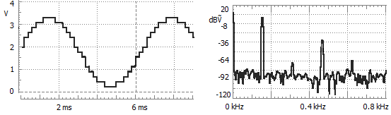
Figure 1.11.1. A 156.25Hz sine wave generated with a 4-bit DAC. The plot on the right is the Fourier Transform(frequency spectrum dB versus kHz) of the data plotted on the left (PicoScope).
: A system collects 1024 data points with a 12-bit ADC at a sampling rate of 10 kHz. A Discrete Fourier Transform is performed on the data. What range of frequencies are represented and what is the frequency resolution
A logic analyzer is essentially a multiple channel digital storage scope with many ways to trigger. The Analog Discovery from Digilent is both a scope and a logic analyzer. Saleae makes an excellent logic analyzer.
All professors teaching embedded systems believe each student should own a
multimeter and a logic analyzer.
As shown in Figure 1.11.2, we can connect the logic analyzer to digital signals that are part of the system, or we can connect the logic analyzer channels to unused microcontroller pins and add software to toggle those pins at strategic times/places. As a troubleshooting aid, it allows the experimenter to observe numerous digital signals at various points in time and thus make decisions based upon such observations. One problem with logic analyzers is the massive amount of information that it generates. To use an analyzer effectively one must learn proper triggering mechanisms to capture data at appropriate times eliminating the need to sift through volumes of output. The logic analyzer figures in this book were collected with the Analog Discovery from Digilent. It is an extremely effective debugging tool.
Maintenance Tip: First, find the things that will break you. Second, break them.
Common error: Sometimes the original system operates properly, and the debugging code has mistakes.
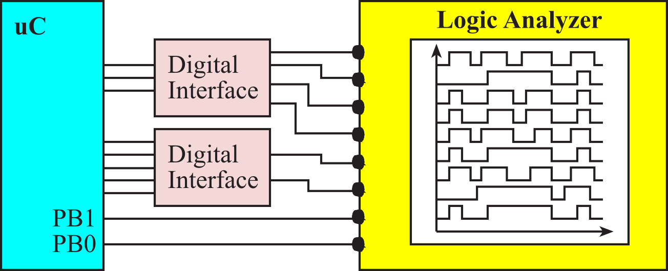
Figure 1.11.2. A logic analyzer and example output. PB1 and PB0 are extra pins just used for debugging.
Figure 1.11.3 shows a logic analyzer output, where signals SSI are outputs to the LCD, and UART is transmission between two microcontroller. However PF3 and PF1 are debugging outputs to measuring timing relationships between software execution and digital I/O. The rising edge of PF1 is used to trigger the data collection.
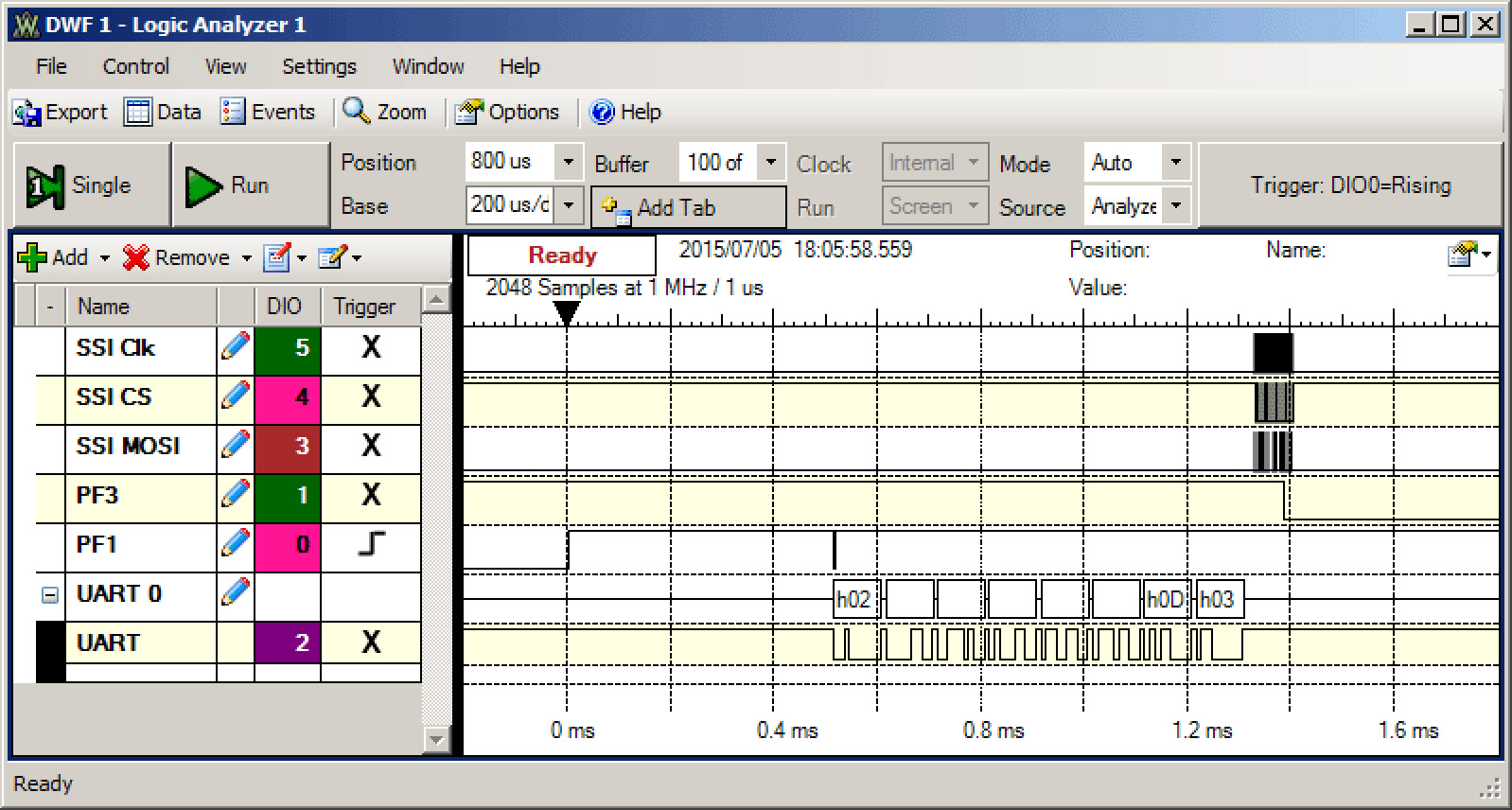
Figure 1.11.3. Analog Discovery logic analyzer output, https://digilent.com/
1.11.2. Debugging Theory
Debugging is an essential component of embedded system design. We need to consider debugging during all phases of the design cycle. It is important to develop a structure or method when verifying system performance. This section will present a number of tools we can use when debugging. Terms such as program testing, diagnostics, performance debugging, functional debugging, tracing, profiling, instrumentation, visualization, optimization, verification, performance measurement, and execution measurement have specialized meanings, but they are also used interchangeably, and they often describe overlapping functions. For example, the terms profiling, tracing, performance measurement, or execution measurement may be used to describe the process of examining a program from a time viewpoint. But, tracing is also a term that may be used to describe the process of monitoring a program state or history for functional errors, or to describe the process of stepping through a program with a debugger. Usage of these terms among researchers and users vary.
Black-box testing is simply observing the inputs and outputs without looking inside. Black-box testing has an important place in debugging a module for its functionality. On the other hand, white-box testing allows you to control and observe the internal workings of a system. A common mistake made by new engineers is to just perform black box testing. Effective debugging uses both. One must always start with black-box testing by subjecting a hardware or software module to appropriate test-cases. Once we document the failed test-cases, we can use them to aid us in effectively performing the task of white-box testing.
We define a debugging instrument as software code
that is added to the program for the purpose of debugging. A print statement is
a common example of an instrument. Using the editor, we add print statements to
our code that either verify proper operation or display run-time errors. A key
to writing good debugging instruments is to provide for a mechanism to reliably
and efficiently remove all them when the debugging is done. Consider the
following mechanisms as you develop your own unique debugging style:
- Place all print statements in a unique column (e.g., first column.), so that the only code that exists in this column will be debugging instruments.
- Define all debugging instruments as functions that all have a specific pattern in their names (e.g., begin with Debug_. In this way, the find/replace mechanism of the editor can be used to find all the calls to the instruments.
- Define the instruments so that they test a run time global flag. When this flag is turned off, the instruments perform no function. Notice that this method leaves a permanent copy of the debugging code in the final system, causing it to suffer a runtime overhead, but the debugging code can be activated dynamically without recompiling. Many commercial software applications utilize this method because it simplifies "on-site" customer support.
- Use conditional compilation (or conditional assembly) to turn on and off the instruments when the software is compiled. When the compiler supports this feature, it can provide both performance and effectiveness.
- Some compilers support a configuration mode that can be set to debug or release. In debug mode, debugging instruments are added. In release mode, the instruments are removed.
: Consider the difference between a runtime flag that activates a debugging command versus a compile-time flag. In both cases it is easy to activate/deactivate the debugging statements. List one factor for which each method is superior to the other.
: What are the advantages of leaving debugging instruments in a final delivered product?
Nonintrusiveness is the characteristic or quality of a debugger that allows the software-hardware system to operate normally as if the debugger did not exist. Conversely, intrusiveness is used as a measure of the degree of perturbation caused in program performance by the debugging instrument itself (Heisenberg Principle). Let t be the time required to execute the instrument and let Δt be the average time in between executions of the instrument. One quantitative measure of intrusiveness is t/Δt, which is the fraction of available processor time used by the debugger. For example, a print statement added to your source code may be very intrusive because it might significantly affect the real-time interaction of the hardware and software. Observing signals that already exist as part of the system with an oscilloscope or logic analyzer is nonintrusive. A debugging instrument is classified as minimally intrusive if it has a nonzero but negligible effect on the system being debugged. In a real microcontroller system, breakpoints and single-stepping are also intrusive, because the real hardware continues to change while the software has stopped. When a program interacts with real-time events, the performance can be significantly altered when using intrusive debugging tools. To be effective we must employ nonintrusive or minimally intrusive methods.
: What does it mean for a debugging instrument to be minimally intrusive? Give both a general answer and a specific criterion.
Although, a wide variety of program monitoring and debugging tools are available today, in practice it is found that an overwhelming majority of users either still prefer or rely mainly upon "rough and ready" manual methods for locating and correcting program errors. These methods include desk-checking, dumps, and print statements, with print statements being one of the most popular manual methods. Manual methods are useful because they are readily available, and they are relatively simple to use. But, the usefulness of manual methods is limited: they tend to be highly intrusive, and they do not provide adequate control over repeatability, event selection, or event isolation. A real-time system, where software execution timing is critical, usually cannot be debugged with simple print statements, because the print statement itself will require too much time to execute.
The first step of debugging is to stabilize the system. In the debugging context, we stabilize the problem by creating a test routine that fixes (or stabilizes) all the inputs. In this way, we can reproduce the exact inputs over and over again. Once stabilized, if we modify the program, we are sure that the change in our outputs is a function of the modification we made in our software and not due to a change in the input parameters.
Acceleration means we will speed up the testing process. When we are testing one module we can increase how fast the functions are called in an attempt to expose possible faults. Furthermore, since we can control the test environment, we will vary the test conditions over a wide range of possible conditions. Stress testing means we run the system beyond the requirements to see at what point it breaks down.
When a system has a small number of possible inputs (e.g.,
less than a million), it makes sense to test them all. When the number of
possible inputs is large we need to choose a set of inputs. Coverage defines the subset of possible inputs selected for testing. A corner case is defined as a situation at the boundary where multiple inputs are at their
maximum or minimum, like the corner of a 3-D cube. At the corner small changes
in input may cause lots of internal and external changes. In particular, we
need to test the cases we think might be difficult (e.g., the clock output
increments one second from 11:59:59 PM December 31, 1999.) There are many ways
to decide on the coverage. We can select values:
- Near the extremes and in the middle
- Most typical of how our clients will properly use the system
- Most typical of how our clients will improperly use the system
- That differ by one
- You know your system will find difficult
- Using a random number generator and performing many tests
To stabilize the system we define a fixed set of inputs to test, run the system on these inputs, and record the outputs. Debugging is a process of finding patterns in the differences between recorded behavior and expected results. The advantage of modular programming is that we can perform modular debugging. We make a list of modules that might be causing the bug. We can then create new test routines to stabilize these modules and debug them one at a time. Unfortunately, sometimes all the modules seem to work, but the combination of modules does not. In this case we study the interfaces between the modules, looking for intended and unintended (e.g., unfriendly code) interactions.
The emergence of concurrent systems (e.g., distributed networks of microcontrollers), optimizing architectures (e.g., pipelines, cache, branch prediction, out of order execution, conditional execution, and multi-core processors), and the increasing need for security and reliably place further demands on debuggers. The complexities introduced by the interaction of multiple events or time dependent processes are much more difficult to debug than errors associated with sequential programs. The behavior of non-real-time sequential programs is reproducible: for a given set of inputs their outputs remain the same. In the case of concurrent or real-time programs this does not hold true. Control over repeatability, event selection, and event isolation is even more important for concurrent or real-time environments.
Sometimes, the meaning and scope of the term debugging itself is not clear. We hold the view that the goal of debugging is to maintain and improve software, and the role of a debugger is to support this endeavor. We define the debugging process as testing, stabilizing, localizing, and correcting errors. And in our opinion, although testing, stabilizing, and localizing errors are important and essential to debugging, they are auxiliary processes: the primary goal of debugging is to remedy faults and verify the system is operating within specifications.
1.11.3. Functional Debugging
Functional debugging involves the verification of input/output parameters. It is a static process where inputs are supplied, the system is run, and the outputs are compared against the expected results. We will present seven methods of functional debugging.
1. Single Stepping or Trace. Many debuggers allow you to set the program counter to a specific address then execute one instruction at a time. StepOver will execute one instruction, unless that instruction is a subroutine call, in which case the simulator will execute the entire subroutine and stop at the instruction following the subroutine call. StepOut assumes the execution has already entered a function and will finish execution of the function and stop at the instruction following the function call.
2. Breakpoints without filtering. The first step of debugging is to stabilize the system with the bug. In the debugging context, we stabilize the problem by creating a test routine that fixes (or stabilizes) all the inputs. In this way, we can reproduce the exact inputs over and over again. Once stabilized, if we modify the program, we are sure that the change in our outputs is a function of the modification we made in our software and not due to a change in the input parameters. A breakpoint is a mechanism to tag places in our software, which when executed will cause the software to stop.
3. Conditional breakpoints. One of the problems with breakpoints is that sometimes we have to observe many breakpoints before the error occurs. One way to deal with this problem is the conditional breakpoint. Add a global variable called count and initialize it to zero in the ritual. Add the following conditional breakpoint to the appropriate location, and run the system again (you can change the 32 to match the situation that causes the error).
if(++count == 32){
breakpoint(); // implemented with BKPT instruction
}
Notice that the breakpoint occurs only on the 32nd time the break is encountered. Any appropriate condition can be substituted.
4. Instrumentation: print statements. The use of print statements is a popular and effective means for functional debugging. The difficulty with print statements in embedded systems is that a standard "printer" may not be available. Another problem with printing is that most embedded systems involve time-dependent interactions with their external environment. The print statement itself may so slow that the debugging instrument itself causes the system to fail. Therefore, the print statement is usually intrusive. One exception to this rule is if the printing channel occurs in the background using interrupts, and the time between print statements (t2) is large compared to the time to execution one print (t1), then the print statements will be minimally intrusive. Nevertheless, this book will focus on debugging methods that do not rely on the availability of a printer.
5. Instrumentation: dump into array without filtering. One of the difficulties with print statements is that they can significantly slow down the execution speed in real-time systems. Many times the bandwidth of the print functions cannot keep pace with data being generated by the debugging process. For example, our system may wish to call a function 1000 times a second (or every 1 ms). If we add print statements to it that require 50 ms to perform, the presence of the print statements will significantly affect the system operation. In this situation, the print statements would be considered extremely intrusive. Another problem with print statements occurs when the system is using the same output hardware for its normal operation, as is required to perform the print function. In this situation, debugger output and normal system output are intertwined.
To solve both these situations, we can add a debugger instrument that dumps strategic information into arrays at run time. We can then observe the contents of the array at a later time. One of the advantages of dumping is that the JTAG debugging allows you to visualize memory even when the program is running.
Assume Happy and Sad are strategic 32-bit variables. The first step when instrumenting a dump is to define a buffer in RAM to save the debugging measurements. The Debug_Cnt will be used to index into the buffers. Debug_Cnt must be initialized to zero, before the debugging begins. The debugging instrument, shown in Program 1.11.1, saves the strategic variables into the buffer.
#define SIZE 100
uint32_t Debug_Buffer[SIZE][2];
unsigned int Debug_Cnt=0;
void Debug_Dump(void){ // dump Happy and Sad
if(Debug_Cnt < SIZE){
Debug_Buffer[Debug_Cnt][0] = Happy;
Debug_Buffer[Debug_Cnt][1] = Sad;
Debug_Cnt++;
}
}
Program 1.11.1. Instrumentation dump without filtering.
Next, you add Debug_Dump(); statements at strategic places within the system. You can either use the debugger to display the results or add software that prints the results after the program has run and stopped. In this way, you can collect information in the exact same manner you would if you were using print statements.
6. Instrumentation: dump into array with filtering. One problem with dumps is that they can generate a tremendous amount of information. If you suspect a certain situation is causing the error, you can add a filter to the instrument. A filter is a software/hardware condition that must be true in order to place data into the array. In this situation, if we suspect the error occurs when the pointer nears the end of the buffer, we could add a filter that saves in the array only when data matches a certain condition. In the example shown in Program 1.11.2, the instrument saves the strategic variables into the buffer only when Sad is greater than 100.
#define SIZE 100
uint32_t Debug_Buffer[SIZE][2];
unsigned int Debug_Cnt=0;
void Debug_FilteredDump(void){ // dump Happy and Sad if Sad > 100
if((Sad > 100)&&(Debug_Cnt < SIZE)){
Debug_Buffer[Debug_Cnt][0] = Happy;
Debug_Buffer[Debug_Cnt][1] = Sad;
Debug_Cnt++;
}
}
Program 1.11.2. Instrumentation dump with filter.
7. Monitor using the LED heartbeat. Another tool that works well for real-time applications is the monitor. A monitor is an independent output process, somewhat like the print statement, but one that executes much faster and thus is much less intrusive. The OLED or LCD can be an effective monitor for small amounts of information if the time between outputs is much larger than the time to output. Another popular monitor is the LED. You can place one or more LEDs on individual otherwise unused output bits. Software toggles these LEDs to let you know what parts of the program are running. An LED is an example of a Boolean monitor or heartbeat. Assume we allocate two pins of the microcontroller, not used for the main system. We can attach LEDs to the pins or we could connect the pins to a logic analyzer or scope. Software defined in Program T.1.2 will toggle the pins. We place the following to statements at strategic places in our system.
Debug_Init(); // call this once
Debug_HeartBeat0(); // toggles one pin
Debug_HeartBeat1(); // toggles the other pin
Program 1.11.3. An LED monitor.
Next, you add Debug_HeartBeat(); statements at strategic places within the system. Port D must be initialized so that bit 1 is an output before the debugging begins. You can either observe the LED directly or look at the LED control signals with a high-speed oscilloscope or logic analyzer. When using LED monitors it is better to modify just the one bit, leaving the other 7 as is. To remove the critical section, we will use bit banding or bit-specific addressing to output to the LED. In this way, you can have multiple monitors on one port.
: Write a debugging instrument that toggles Port A bit 3, using bit-specific addressing. Assume PA3 is already initialized as an output.
1.11.4. Performance Debugging
Performance debugging or dynamic efficiency involves the verification of timing behavior of our system. It is a dynamic process where the system is run, and the dynamic behavior of the system is compared against the expected results. We will present three methods of performance debugging, then apply the techniques to measure execution speed.
1. Counting bus cycles. For simple programs with little and no branching and for simple microcontrollers, we can estimate the execution speed by looking at the assembly code and adding up the time to execute each instruction.
2. Instrumentation measuring with an independent counter. SysTick is a 24-bit counter decremented every bus clock. It automatically rolls over when it gets to 0. If we are sure the execution speed of our function is less than 224 bus cycles, we can use this timer to collect timing information with only a minimal amount of intrusiveness.
3. Instrumentation Output Port. Another method to measure real-time execution involves an output port and an oscilloscope. Connect a microcontroller output bit to your scope. Add debugging instruments that set/clear these output bits at strategic places. Remember to set the port's direction register to 1. Assume an oscilloscope is attached to Port B bit 1. Port B must be initialized so that bit 1 is an output before the debugging begins. Program 1.11.4 can be used to set and clear the bit.
|
// TM4C123 |
// MSPM0G3507 |
Program 1.11.4. Instrumentation output port.
Next, you add Debug_Set(); and Debug_Clear(); statements before and after the code you wish to measure. You can observe the signal with a high-speed oscilloscope or logic analyzer.
Debug_Set();
Stuff(); // User code to be measured
Debug_Clear();
To illustrate these three methods, we will consider measuring the execution time of an integer square root function as presented Program 1.11.5.
The first method is to count bus cycles using the assembly listing. This approach is only appropriate for very short programs, and becomes difficult for long programs with many conditional branch instructions. The time to execute each assembly instruction can be found in the Table 3.1 in the Cortex-M Technical Reference Manual. Because of the complexity of the ARM Cortex-M, this method is only approximate. For example, the time to execute a divide depends on the data, and the time to execute a branch depends on the alignment of the instruction pipeline. A portion of the assembly output generated by the ARM Keil uVision compiler is presented on the left side of Program 1.11.5. Notice that the total cycle count for could range from 155 to 353 cycles. At 16 MHz the execution time could range from 9.69 to 22.1 µs. For most programs it is actually very difficult to get an accurate time measurement using this technique.
|
sqrt MOV r1,r0 [1] MOVS r3,#0x01 [1] ADD r0,r3,r1,LSR #4 [1] MOVS r2,#0x10 [1] B chck [2-4] loop MLA r3,r0,r0,r1 [2]*16 UDIV r3,r3,r0 [2-12]*16 LSRS r0,r3,#1 [1]*16 SUBS r2,r2,#1 [1]*16 chck CMP r2,#0x00 [1]*17 BNE loop [2-4]*17 BX lr [2-4] |
// Newton's method // s is an integer // sqrt(s) is an integer uint32_t sqrt(uint32_t s){ uint32_t t; // t*t becomes s int n; // loop counter t = s/10+1; // initial guess for(n = 16; n; --n){ // will finish t = ((t*t+s)/t)/2; } return t; } |
Program 1.11.5. Assembly listing and C code for a sqrt function.
The second method uses an internal timer called SysTick. The ARM Cortex-M microcontrollers provide the 24-bit SysTick register (NVIC_ST_CURRENT_R) that is automatically decremented at the bus frequency. When the counter hits zero, it is reloaded to 0xFFFFFF and continues to count down. If we are sure the function will complete in a time less than 224 bus cycles, then the internal timer can be used to measure execution speed empirically. The code in Program 1.11.6 first reads the SysTick counter, executes the function, and then reads the SysTick counter again. The elapsed time is the difference in the counter before and after. Since the execution speed may be dependent on the input data, it is often wise to measure the execution speed for a wide range of input parameters. There is a slight overhead in the measurement process itself. To be accurate, you could measure this overhead and subtract it off your measurements. In this case, a constant 4 is subtracted so that if the call to the function were completely removed the elapsed time would return 0. Notice that in this example, the total time including parameter passing is measured. Experimental results show this function executes in 204 bus cycles. At 16 MHz, this corresponds to 12.75 µs.
uint32_t Before, Elapsed;
void main(void){ volatile uint32_t Out;
SysTick_Init(); // Program 1.9.1
Before = NVIC_ST_CURRENT_R;
Out = sqrt(230400);
Elapsed = (Before - NVIC_ST_CURRENT_R - 4)&0x00FFFFFF;
}
Program 1.11.6: Empirical measurement of dynamic efficiency.
The third technique can be used in situations where a timer is unavailable or where the execution time might be larger than 224 counts. In this empirical technique we attach an unused output pin to an oscilloscope or to a logic analyzer. We will set the pin high before the call to the function and set the pin low after the function call. In this way a pulse is created on the digital output with a duration equal to the execution time of the function. We assume Port D is available, and bit 1 is connected to the scope. By placing the function call in a loop, the scope can be triggered. With a storage scope or logic analyzer, the function need be called only once. Together with an oscilloscope or logic analyzer, Program 1.11.7 measures the execution time of the function sqrt (Figure 1.11.4). We stabilize the system by calling it over and over. Using the scope, we can measure the width of the pulse on PD1, which will be execution time of the function sqrt. Running at 16 MHz, the results in Figure 1.11.4 show it takes 13 µs to execute sqrt(230400), which is 208 bus cycles.
int main(void){ uint32_t Out;
PortB_Init();
while(1){
Debug_Set(); // Program 1.11.4
Out = sqrt(230400);
Debug_Clear(); // Program 1.11.4
}
}
Program 1.11.7. Another empirical measurement of dynamic efficiency.
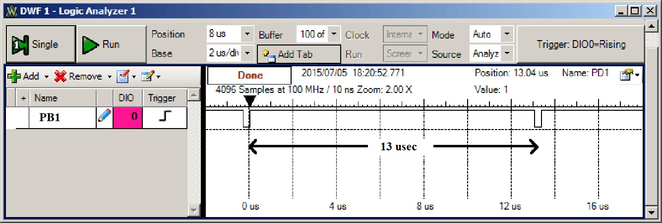
Figure 1.11.4. Logic analyzer output measured from Program 1.11.7 using an Analog Discovery.
: If you were to remove the Out=sqrt(230400); line in Program 1.11.7, what would you expect the pulse width on PB1 to be? Why does Program 1.11.6 yield a result smaller than Program 1.11.7?
1.11.5. Profiling
Profiling is a type of performance debugging that collects the time history of program execution. Profiling measures where and when our software executes. It could also include what data is being processed. For example, if we could collect the time-dependent behavior of the program counter, then we could see the execution patterns of our software. We can profile the execution of a multiple thread software system to detect reentrant activity.
Profiling using a software dump to study execution pattern. In this section, we will discuss software instruments that study the execution pattern of our software. In order to collect information concerning execution we will add debugging instruments that save the time and location in arrays (Program 1.11.8). By observing these data, we can determine both a time profile (when) and an execution profile (where) of the software execution. Running this profile revealed the sequence of places as 0, 1, 2, 2, 2, 2, 2, 2, 2, 2, 2, 2, 2, 2, 2, 2, 2, 2, and 3. Each call to Debug_Profile requires 32 cycles to execute. Therefore, this instrument is a lot less intrusive than a print statement.
uint32_t Debug_time[20];
uint8_t Debug_place[20];
uint32_t n;
void Debug_Profile(uint8_t p){
if(n < 20){
Debug_time[n] = NVIC_ST_CURRENT_R; // record current time
Debug_place[n] = p;
n++;
}
}
uint32_t sqrt(uint32_t s){
uint32_t t; // t*t becomes s
int n; // loop counter
Debug_Profile(0);
t = s/10+1; // initial guess
Debug_Profile(1);
for(n = 16; n; --n){ // will finish
Debug_Profile(2);
t = ((t*t+s)/t)/2;
}
Debug_Profile(3);
return t;
}
Program 1.11.8: A time/position profile dumping into a data array.
Profiling using an Output Port. In this section, we will discuss a hardware/software combination to visualize program activity. Our debugging instrument will set output port bits B3-B0 (Program 1.11.9). We will place these instruments at strategic places in the software. In particular, we will output 1, 2, 4, or 8 to Port D, where each bit uniquely specifies where in the program we are executing (Figure 1.11.5). We connect the four output pins to a logic analyzer and observe the program activity. Each debugging instrument requires only 4 cycles to execute. So the profile in Program 1.11.9 is less intrusive than the one in Program 1.11.8. In particular, notice the execution speed of the sqrt function only increases from 13 to 16 μs on the TM4C123. This 3-μs execution penalty is a measure of the intrusiveness of the debugging activity.
|
// TM4C123 |
// MSPM0G3507 |
uint32_t sqrt(uint32_t s){
uint32_t t; // t*t becomes s
int n; // loop counter
Profile(1);
t = s/10+1; // initial guess
Profile(2);
for(n = 16; n; --n){ // will finish
Profile(4);
t = ((t*t+s)/t)/2;
Profile(8);
}
Profile(0);
return t;
}
Program 1.11.9: A time/position profile using four output bits.
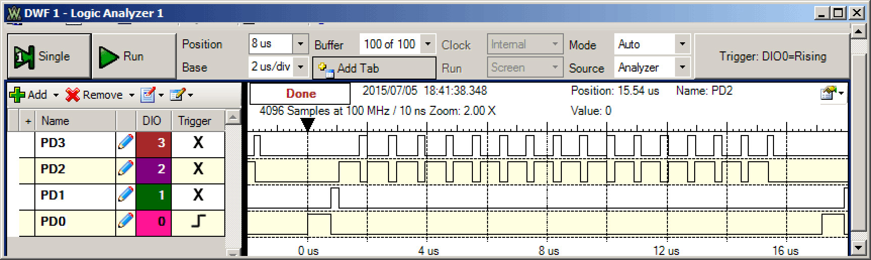
Figure 1.11.5. Logic analyzer output measured from Program 1.11.9 using an Analog Discovery.
Thread Profile. When more than one program (multiple threads) is running, you could toggle a GPIO output in each thread to visualize which thread is currently running. For each thread, we assign one output pin. The debugging instrument would toggle the pin while that thread is running. We would then connect the output pins to a logic analyzer to visualize in real time the thread that is currently running. Figures 1.11.6 and 1.11.7 show the logic analyzer traces when running Program 1.9.2. When zoomed out, we can see the interrupt occurs every 1 ms. When zoomed in, we can see the main program halts during the ISR invocation.
|
// TM4C123 |
// MSPM0G3507 |
volatile uint32_t Counts=0; // time in msec
void SysTick_Handler(void){
Toggle1(); // toggle PB1
Counts = Counts + 1;
}
int main(void){ // running at 16 MHz
DisableInterrupts(); // __disable_irq(); on MSPM0
Counts = 0;
PortB_Init; // make PB1,PB0 output
SysTick_Init(16000,2); // initialize SysTick
timer, every 1ms
EnableInterrupts(); // __enable_irq(); on MSPM0
while(1){ //
interrupts every 1ms, 500 Hz flash
Toggle0(); // toggle PB0
}
}
Program 1.9.2 (repeated). Implementation of a periodic interrupt using SysTick.
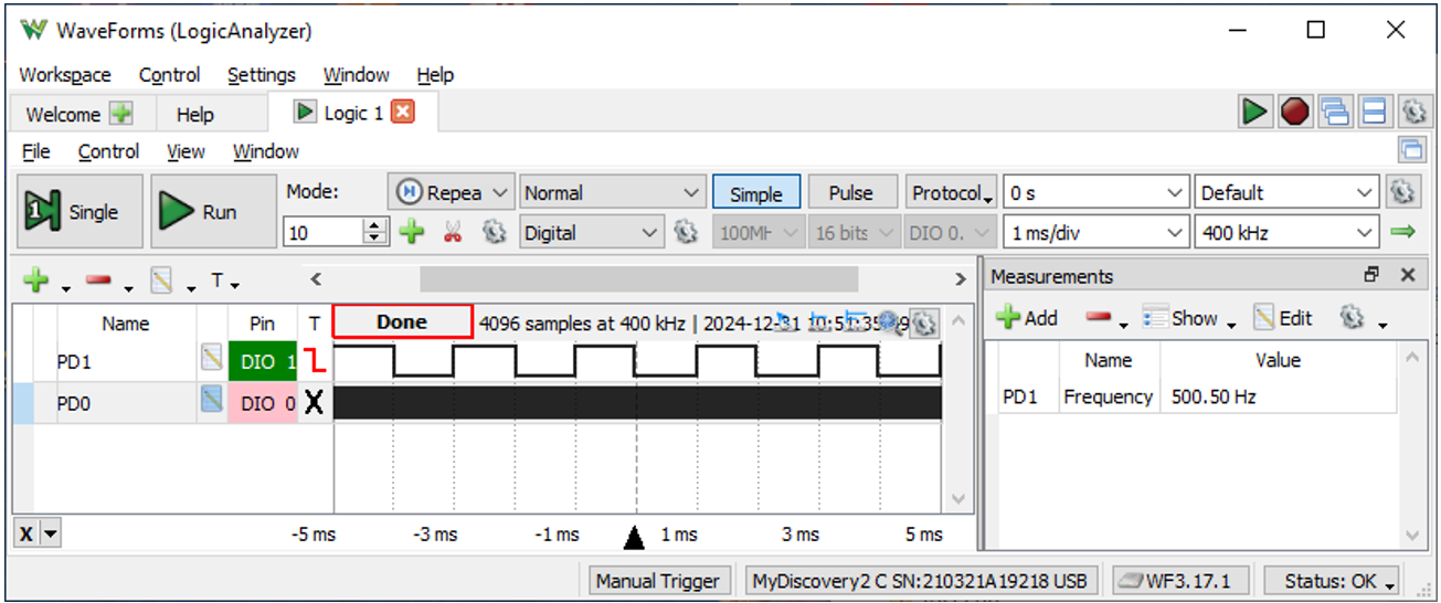
Figure 1.11.6. Logic analyzer outputs measured from Program 1.9.2 using an Analog Discovery. Zoomed out view to see ISR runs every 1ms.
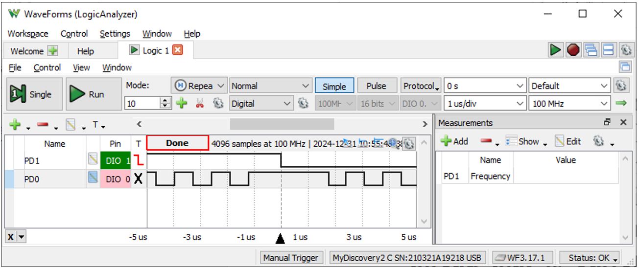
Figure 1.11.7. Logic analyzer outputs measured from Program 1.9.2 using an Analog Discovery. Zoomed out view to see main program is halted during interrupt service.
1.12. Lab 1
Lab 1 for this course can be downloaded from this link Lab01.docx
Each lab also has a report, which can be downloaded from this link Lab01Report.docx
This work is based on the course ECE445L
taught at the University of Texas at Austin. This course was developed by Jonathan Valvano, Mark McDermott, and Bill Bard.
Reprinted with approval from Embedded Systems: Real-Time Interfacing to ARM Cortex-M Microcontrollers, ISBN-13: 978-1463590154

Embedded Systems: Real-Time Interfacing to ARM Cortex-M Microcontrollers by Jonathan Valvano is
licensed under a Creative
Commons
Attribution-NonCommercial-NoDerivatives 4.0 International License.