Appendix
M. MSPM0G3507 I/O Registers
Jonathan
Valvano and Mark McDermott
This chapter describes the MSPM0G3507 I/O registers used in this book. It is not intended to replace the MSPM0 technical reference manual, but to serve as a quick reference for the specific registers used in this class.
Table of Contents:
- M.0. Nested Vectored Interrupt Controller (NVIC)
- M.1. GPIO Programming
- M.2. ADC Programming
- M.3. Periodic Timer Interrupts
- M.4. UART
- M.5. Synchronous Transmission and Receiving using the SPI
- M.6. Inter-Integrated Circuit (I2C) Interface
- M.7. Edge-triggered Interrupts
- M.8. Pulse Width Modulation
- M.9. Input Capture
- M.10. Controller Area Network (CAN)
M.0. Nested Vectored Interrupt Controller (NVIC)
On the ARM Cortex-M processor, exceptions include resets, software interrupts and hardware interrupts. Interrupts on the Cortex-M are controlled by the Nested Vectored Interrupt Controller (NVIC). Each exception has an associated 32-bit vector that points to the memory location where the ISR that handles the exception is located. Vectors are stored in ROM at the beginning of memory. Program M.0.1 shows the first few vectors as defined in the startup_mspm0g3507_ticlang.c file. ROM location 0x0000.0000 has the initial stack pointer, and location 0x0000.0004 contains the initial program counter, which is called the reset vector. It points to a function called the reset handler, which is the first thing executed following reset. There are up to 240 possible interrupt sources and their 32-bit vectors are listed in order starting with location 0x0000.0008. From a programming perspective, we can attach ISRs to interrupts by writing the ISRs as regular assembly subroutines or C functions with no input or output parameters and editing the startup_mspm0g3507_ticlang.c file to specify those functions for the appropriate interrupt. For example, if we wrote a Port A edge-triggered interrupt service routine named GROUP0ISR, then we would replace GROUP0_IRQHandler with GROUP0ISR. In this class, we will write our ISRs using standard function names so that the startup_mspm0g3507_ticlang.c file need not be edited. I.e., we will simply name the ISR for edge-triggered interrupts on Port A as GROUP0_IRQHandler. The ISR for this interrupt is a 32-bit pointer located at ROM address 0x0000.0040. Because the vectors are in ROM, this linkage is defined at compile time and not at run time. For more details see the startup_mspm0g3507_ticlang.c files within the interrupt examples posted on the book web site.
Video M.0.1. Interrupt Vector Table
void (* const interruptVectors[])(void) = {
(void (*)(void))((uint32_t)&__STACK_END), /* initial SP */
Reset_Handler, /* The reset handler */
NMI_Handler, /* The NMI handler */
HardFault_Handler, /* The hard fault handler */
0, /* Reserved */
0, /* Reserved */
0, /* Reserved */
0, /* Reserved */
0, /* Reserved */
0, /* Reserved */
0, /* Reserved */
SVC_Handler, /* SVCall handler */
0, /* Reserved */
0, /* Reserved */
PendSV_Handler, /* The PendSV handler */
SysTick_Handler, /* SysTick handler */
GROUP0_IRQHandler, /* GROUP0 interrupt handler */
GROUP1_IRQHandler, /* GROUP1 interrupt handler */
TIMG8_IRQHandler, /* TIMG8 interrupt handler */
UART3_IRQHandler, /* UART3 interrupt handler */
ADC0_IRQHandler, /* ADC0 interrupt handler */
ADC1_IRQHandler, /* ADC1 interrupt handler */
CANFD0_IRQHandler, /* CANFD0 interrupt handler */
DAC0_IRQHandler, /* DAC0 interrupt handler */
0, /* Reserved */
SPI0_IRQHandler, /* SPI0 interrupt handler */
SPI1_IRQHandler, /* SPI1 interrupt handler */
0, /* Reserved */
0, /* Reserved */
UART1_IRQHandler, /* UART1 interrupt handler */
UART2_IRQHandler, /* UART2 interrupt handler */
UART0_IRQHandler, /* UART0 interrupt handler */
TIMG0_IRQHandler, /* TIMG0 interrupt handler */
TIMG6_IRQHandler, /* TIMG6 interrupt handler */
TIMA0_IRQHandler, /* TIMA0 interrupt handler */
TIMA1_IRQHandler, /* TIMA1 interrupt handler */
TIMG7_IRQHandler, /* TIMG7 interrupt handler */
TIMG12_IRQHandler, /* TIMG12 interrupt handler */
Program M.0.1. Software syntax to set the interrupt vectors for the MSPM0 (only some vectors are shown, see the startup_mspm0g3507_ticlang.c file for a complete list).
Program M.0.2 shows that the syntax for an ISR looks like a function with no parameters. Notice that each ISR (except for SysTick) must acknowledge the interrupt in software by clearing the flag that caused the interrupt. In Program M.0.2, we assume the interrupt was caused by an edge on PB21 input, so writing to the ICLR register will clear trigger flag 21.
void GROUP1_IRQHandler(void){
GPIOB->CPU_INT.ICLR = 0x00200000; // ack, clear interrupt flag21
// stuff
}
Program M.0.2. Typical interrupt service routine.
| Vector address | Number | IRQ | ISR name | Usage |
| 0x0000002C | 11 | -5 | SVC_Handler | Software interrupt |
| 0x00000038 | 14 | -2 | PendSV_Handler | Software interrupt to OS |
| 0x0000003C | 15 | -1 | SysTick_Handler | Periodic timer |
| 0x00000040 | 16 | 0 | GROUP0_IRQHandler | Port A edge triggered |
| 0x00000044 | 17 | 1 | GROUP1_IRQHandler | Port B edge triggered |
| 0x00000048 | 18 | 2 | TIMG8_IRQHandler | Timer |
| 0x0000004C | 19 | 3 | UART3_IRQHandler | Asynchronous serial I/O |
| 0x00000050 | 20 | 4 | ADC0_IRQHandler | Analog to digital |
| 0x00000054 | 21 | 5 | ADC1_IRQHandler | Analog to digital |
| 0x00000058 | 22 | 6 | CANFD0_IRQHandler | Controller area network |
| 0x0000005C | 23 | 7 | DAC0_IRQHandler | Digital to analog |
| 0x00000064 | 25 | 9 | SPI0_IRQHandler | Synchronous serial I/O |
| 0x00000068 | 26 | 10 | SPI1_IRQHandler | Synchronous serial I/O |
| 0x00000074 | 29 | 13 | UART1_IRQHandler | Asynchronous serial I/O |
| 0x00000078 | 30 | 14 | UART2_IRQHandler | Asynchronous serial I/O |
| 0x0000007C | 31 | 15 | UART0_IRQHandler | Asynchronous serial I/O |
| 0x00000080 | 32 | 16 | TIMG0_IRQHandler | Timer |
| 0x00000084 | 33 | 17 | TIMG6_IRQHandler | Timer |
| 0x00000088 | 34 | 18 | TIMA0_IRQHandler | Timer |
| 0x0000008C | 35 | 19 | TIMA1_IRQHandler | Timer |
| 0x00000090 | 36 | 20 | TIMG7_IRQHandler | Timer |
| 0x00000094 | 37 | 21 | TIMG12_IRQHandler | Timer |
Table M.0.1. Some of the interrupt vectors for the MSPM0.
: Where is the vector for SysTick? What should you call the name of software function which is the SysTick interrupt service routine?
To activate an interrupt source we need to set its priority and enable that source in the NVIC. This activation is in addition to the arm and enable steps. Table M.0.1 lists some of the interrupt sources available on the MSPM0 family of microcontrollers. Interrupt numbers 0 to 15 contain the faults, software interrupt and SysTick. SysTick does not require access to NVIC->ISER to enable. The SysTick priority is set in bits 31 and 30 of SCB->SHP[1].
Table M.0.2 shows some of the priority registers on the NVIC. Each register contains an 8-bit priority field for four devices. On the MSPM0 microcontrollers, only the top two bits of the 8-bit field are used. This allows us to specify the interrupt priority level for each device from 0 to 3, with 0 being the highest priority. The interrupt number (number column in Table M.0.1) is loaded into the IPSR register. The servicing of interrupts does not set the I bit in the PRIMASK, so a higher priority interrupt can suspend the execution of a lower priority ISR. If a request of equal or lower priority is generated while an ISR is being executed, that request is postponed until the ISR is completed. In particular, those devices that need prompt service should be given high priority.
| ISR name | NVIC priority | Priority bits | NVIC enable | Enable bit |
| PendSV_Handler | SCB->SHP[1] | 23 - 22 | -- | -- |
| SysTick_Handler | SCB->SHP[1] | 31 - 30 | -- | -- |
| GROUP0_IRQHandler | NVIC->IP[0] | 7 - 6 | NVIC->ISER[0] | 0 |
| GROUP1_IRQHandler | NVIC->IP[0] | 15 - 14 | NVIC->ISER[0] | 1 |
| TIMG8_IRQHandler | NVIC->IP[0] | 23 - 22 | NVIC->ISER[0] | 2 |
| UART3_IRQHandler | NVIC->IP[0] | 31 - 30 | NVIC->ISER[0] | 3 |
| ADC0_IRQHandler | NVIC->IP[1] | 7 - 6 | NVIC->ISER[0] | 4 |
| ADC1_IRQHandler | NVIC->IP[1] | 15 - 14 | NVIC->ISER[0] | 5 |
| CANFD0_IRQHandler | NVIC->IP[1] | 23 - 22 | NVIC->ISER[0] | 6 |
| DAC0_IRQHandler | NVIC->IP[1] | 31 - 30 | NVIC->ISER[0] | 7 |
| SPI0_IRQHandler | NVIC->IP[2] | 15 - 14 | NVIC->ISER[0] | 9 |
| SPI1_IRQHandler | NVIC->IP[2] | 23 - 22 | NVIC->ISER[0] | 10 |
| UART1_IRQHandler | NVIC->IP[3] | 15 - 14 | NVIC->ISER[0] | 13 |
| UART2_IRQHandler | NVIC->IP[3] | 23 - 22 | NVIC->ISER[0] | 14 |
| UART0_IRQHandler | NVIC->IP[3] | 31 - 30 | NVIC->ISER[0] | 15 |
| TIMG0_IRQHandler | NVIC->IP[4] | 7 - 6 | NVIC->ISER[0] | 16 |
| TIMG6_IRQHandler | NVIC->IP[4] | 15 - 14 | NVIC->ISER[0] | 17 |
| TIMA0_IRQHandler | NVIC->IP[4] | 23 - 22 | NVIC->ISER[0] | 18 |
| TIMA1_IRQHandler | NVIC->IP[4] | 31 - 30 | NVIC->ISER[0] | 19 |
| TIMG7_IRQHandler | NVIC->IP[5] | 7 - 6 | NVIC->ISER[0] | 20 |
| TIMG12_IRQHandler | NVIC->IP[5] | 15 - 14 | NVIC->ISER[0] | 21 |
Table M.0.2. The MSPM0 NVIC registers. Each register is 32 bits wide. Bits not shown are zero.
The NVIC->ISER[0] register contains one bit for
each IRQ number from 0 to 31. We write one to the corresponding bit
of NVIC->ISER[0] to enable that IRQ. Writing zeros to NVIC->ISER[0] has no affect. So,
NVIC->ISER[0] = 1;
will enable GROUP0 (IRQ=0), without affecting the other 31 interrupts.
The NVIC->ICER[0] register also contains one bit for
each IRQ number from 0 to 31. We write one to the corresponding bit
of NVIC->ICER[0] to disable that IRQ, without affecting the other 31 interrupts.
Writing zeros to NVIC->ISER[0] has no affect. So,
NVIC->ISER[0] = 1;
will disable GROUP0 (IRQ=0).
Priority determines the order of service when two or more requests are made simultaneously. Priority also allows a higher priority request to suspend a lower priority request currently being processed. Usually, if two requests have the same priority, we do not allow them to interrupt each other. NVIC assigns a priority level to each interrupt trigger. This mechanism allows a higher priority trigger to interrupt the ISR of a lower priority request. Conversely, if a lower priority request occurs while running an ISR of a higher priority trigger, it will be postponed until the higher priority service is complete.
: Consider using TimerG0 for a periodic interrupt. How would you set its priority to 1?
: Consider using TimerG0 for a periodic interrupt. How would you enable TimerG0 in the NVIC?
: What does this code do? SCB->SHP[1]=(SCB->SHP[1]&(~0xC0000000))|(2<<30);
: Where are the priority bits for SysTick?
: Where are the priority bits for Timer A0?
Observation: There are many interrupt sources, but an effective system will use only a few.
Program M.0.3 gives the definitions the Clang compiler uses that allow the software to enable and disable interrupts. The CPSIE I instruction clears the I bit, enabling interrrupts. The CPSID I instruction sets the I bit, disabling interrrupts. The WFI instruction goes into low power sleep mode and wakes up on the next interrupt. The wait for interrupt can be used to place the processor in low-power sleep mode while it waits for an interrupt.
__STATIC_FORCEINLINE void __enable_irq(void){
__ASM volatile ("cpsie i" : : : "memory");
}
__STATIC_FORCEINLINE void __disable_irq(void){
__ASM volatile ("cpsid i" : : : "memory");
}
__STATIC_FORCEINLINE void __wfi(void){
__ASM volatile ("wfi" : : : "memory");
}
Program M.0.3. Functions needed for interrupt enabling and disabling.
M.1. GPIO Programming
M.1.1. I/O Registers
An I/O register is a location in memory with which software can interface with the I/O port, see Table M.1.1. On most embedded microcontrollers, the I/O ports are memory mapped. This means the software can access an input/output port simply by reading from or writing to the appropriate address. It is important to realize that even though I/O operations "look" like reads and writes to memory variables, the I/O ports often DO NOT act like memory. For example, some bits are read-only, some are write-only, some can only be cleared, others can only be set, and some bits cannot be modified. There are include statements for both assembly and C that will define symbolic names for the I/O registers as their corresponding addresses. To make our software easier to understand we will use the symbolic definitions for the I/O ports, like GPIOA_DOUT31_0, and not the specific address, like 0x400A1280.
| Address | Access | 31 | ... | 28 | 27 | ... | 1 | 0 | Name |
| 0x400A1280 | R/W | DIO31 | ... | DIO28 | DIO27 | ... | DIO1 | DIO0 | GPIOA_DOUT31_0 |
| 0x400A1380 | R | DIO31 | ... | DIO28 | DIO27 | ... | DIO1 | DIO0 | GPIOA_DIN31_0 |
| 0x400A3280 | R/W | - | - | - | DIO27 | ... | DIO1 | DIO0 | GPIOB_DOUT31_0 |
| 0x400A3380 | R | - | - | - | DIO27 | ... | DIO1 | DIO0 | GPIOB_DIN31_0 |
Table M.1.1. I/O registers to perform input/output to Ports A and B.
There are many more registers with which we could perform I/O, but we will begin with these simple interactions:
- Read from GPIOA_DIN31_0 gets the current values of the input pins of Port A
- Write to GPIOA_DOUT31_0 sets the output pins of Port A
- Read from GPIOA_DOUT31_0 gets the last value written to GPIOA->DOUT31_0
- Read from GPIOB_DIN31_0 gets the current values of the input pins of Port B
- Write to GPIOB_DOUT31_0 sets the output pins of Port B
- Read from GPIOB_DOUT31_0 gets the last value written to GPIOB->DOUT31_0
The DIN31_0 register is read only. Writing to DIN31_0 has no effect. The DOUT31_0 register is read/write. The register DOUT31_0 does behave like regular memory.
The DOUTSET31_0 DOUTCLR31_0 DOUTTGL31_0 registers are write only, see Table M.1.2. Reading from these registers has no effect. Writing 0's to these registers have no effect. Writing 1's to bits in these registers will modify the corresponding output pins. We use these three registers when different unrelated software modules need to access the same GPIO port.
| Address | Access | 31 | ... | 28 | 27 | ... | 1 | 0 | Name |
| 0x400A1290 | W | DIO31 | ... | DIO28 | DIO27 | ... | DIO1 | DIO0 | GPIOA_DOUTSET31_0 |
| 0x400A12A0 | W | DIO31 | ... | DIO28 | DIO27 | ... | DIO1 | DIO0 | GPIOA_DOUTCLR31_0 |
| 0x400A12B0 | W | DIO31 | ... | DIO28 | DIO27 | ... | DIO1 | DIO0 | GPIOA_DOUTTGL31_0 |
| 0x400A3290 | W | - | - | - | DIO27 | ... | DIO1 | DIO0 | GPIOB_DOUTSET31_0 |
| 0x400A32A0 | W | - | - | - | DIO27 | ... | DIO1 | DIO0 | GPIOB_DOUTCLR31_0 |
| 0x400A32B0 | W | - | - | - | DIO27 | ... | DIO1 | DIO0 | GPIOB_DOUTTGL31_0 |
Table M.1.2. I/O registers to perform friendly output.
- Write 1s to DOUTSET31_0 to make the output pins go high
- Write 1s to DOUTCLR31_0 to make the output pins go low
- Write 1s to DOUTTGL31_0 to toggle the output pins (invert from 0 to 1 or 1 to 0)
The DOE31_0 register is configured once during initialization, see Table M.1.3.
| Address | Access | 31 | ... | 28 | 27 | ... | 1 | 0 | Name |
| 0x400A12C0 | R/W | DIO31 | ... | DIO28 | DIO27 | ... | DIO1 | DIO0 | GPIOA_DOE31_0 |
| 0x400A32C0 | R/W | - | - | - | DIO27 | ... | DIO1 | DIO0 | GPIOB_DOE31_0 |
Table M.1.3. We set bits in the Data output enable register make that GPIO pin an output.
Each of the 60 I/O pins on the MSPM0G3507 has a 32-bit Pin Control Management Register (PINCM). We write to this register once during initialization to configure the mode. Table M.1.4 shows some of the bits we will configure. We clear the PF field to turn off a pin, we set PF=00001 for GPIO, and Table M.1.5 shows the PF field for the alternate functions available for each pin.
| Name | Pin | ... | 18 | 17 | 18 | ... | 7 | 6 | 5-0 |
| IOMUXPA0 | PA0 | ... | INENA | PIPU | PIPD | ... | PC | - | PF |
| IOMUXPA1 | PA1 | ... | INENA | PIPU | PIPD | ... | PC | - | PF |
| ... | |||||||||
| IOMUXPB26 | PB26 | ... | INENA | PIPU | PIPD | ... | PC | - | PF |
| IOMUXPB27 | PB27 | ... | INENA | PIPU | PIPD | ... | PC | - | PF |
Table M.1.4. Each port pin has a separate Pin Control Management Register, also called IOMUX.
- We set bit 18 INENA to specify the pin as input
- We set bit 17 PIPU to enable a pullup resistor on the input
- We set bit 16 PIPD to enable a pulldown resistor on the input
- We set bit 7 PC to allow software to input/output with the pin
- We set bits 5:0 PF to 00001 to specify GPIO mode.
|
PINCM |
Pin |
Mode2 |
Mode3 |
Mode4 |
Mode5 |
Mode6 |
Mode7 |
Mode8 |
Mode9 |
|
1 |
PA0 |
UART0_TX |
I2C0_SDA |
TIMA0_C0 |
TIMA_FAL1 |
TIMG8_C1 |
FCC_IN |
||
|
2 |
PA1 |
UART0_RX |
I2C0_SCL |
TIMA0_C1 |
TIMA_FAL2 |
TIMG8_IDX |
TIMG8_C0 |
||
|
7 |
PA2 |
TIMG8_C1 |
SPI0_CS0 |
TIMG7_C1 |
SPI1_CS0 |
||||
|
8 |
PA3 |
TIMG8_C0 |
SPI0_CS1 |
UART2_CTS |
TIMA0_C2 |
COMP1_OUT |
TIMG7_C0 |
TIMA0_C1 |
I2C1_SDA |
|
9 |
PA4 |
TIMG8_C1 |
SPI0_POCI |
UART2_RTS |
TIMA0_C3 |
LFCLK_IN |
TIMG7_C1 |
TIMA0_C1N |
I2C1_SCL |
|
10 |
PA5 |
TIMG8_C0 |
SPI0_PICO |
TIMA_FAL1 |
TIMG0_C0 |
TIMG6_C0 |
FCC_IN |
||
|
11 |
PA6 |
TIMG8_C1 |
SPI0_SCK |
TIMA_FAL0 |
TIMG0_C1 |
HFCLK_IN |
TIMG6_C1 |
TIMA0_C2N |
|
|
14 |
PA7 |
COMP0_OUT |
CLK_OUT |
TIMG8_C0 |
TIMA0_C2 |
TIMG8_IDX |
TIMG7_C1 |
TIMA0_C1 |
|
|
19 |
PA8 |
UART1_TX |
SPI0_CS0 |
UART0_RTS |
TIMA0_C0 |
TIMA1_C0N |
|||
|
20 |
PA9 |
UART1_RX |
SPI0_PICO |
UART0_CTS |
TIMA0_C1 |
RTC_OUT |
TIMA0_C0N |
TIMA1_C1N |
CLK_OUT |
|
21 |
PA10 |
UART0_TX |
SPI0_POCI |
I2C0_SDA |
TIMA1_C0 |
TIMG12_C0 |
TIMA0_C2 |
I2C1_SDA |
CLK_OUT |
|
22 |
PA11 |
UART0_RX |
SPI0_SCK |
I2C0_SCL |
TIMA1_C1 |
COMP0_OUT |
TIMA0_C2N |
I2C1_SCL |
|
|
34 |
PA12 |
UART3_CTS |
SPI0_SCK |
TIMG0_C0 |
CAN_TX |
TIMA0_C3 |
FCC_IN |
||
|
35 |
PA13 |
UART3_RTS |
SPI0_POCI |
UART3_RX |
TIMG0_C1 |
CAN_RX |
TIMA0_C3N |
||
|
36 |
PA14 |
UART0_CTS |
SPI0_PICO |
UART3_TX |
TIMG12_C0 |
CLK_OUT |
|||
|
37 |
PA15 |
UART0_RTS |
SPI1_CS2 |
I2C1_SCL |
TIMA1_C0 |
TIMG8_IDX |
TIMA1_C0N |
TIMA0_C2 |
|
|
38 |
PA16 |
COMP2_OUT |
SPI1_POCI |
I2C1_SDA |
TIMA1_C1 |
TIMA1_C1N |
TIMA0_C2N |
FCC_IN |
|
|
39 |
PA17 |
UART1_TX |
SPI1_SCK |
I2C1_SCL |
TIMA0_C3 |
TIMG7_C0 |
TIMA1_C0 |
||
|
40 |
PA18 |
UART1_RX |
SPI1_PICO |
I2C1_SDA |
TIMA0_C3N |
TIMG7_C1 |
TIMA1_C1 |
||
|
41 |
PA19 |
SWDIO |
|||||||
|
42 |
PA20 |
SWCLK |
|||||||
|
46 |
PA21 |
UART2_TX |
TIMG8_C0 |
UART1_CTS |
TIMA0_C0 |
TIMG6_C0 |
|||
|
47 |
PA22 |
UART2_RX |
TIMG8_C1 |
UART1_RTS |
TIMA0_C1 |
CLK_OUT |
TIMA0_C0N |
TIMG6_C1 |
|
|
53 |
PA23 |
UART2_TX |
SPI0_CS3 |
TIMA0_C3 |
TIMG0_C0 |
UART3_CTS |
TIMG7_C0 |
TIMG8_C0 |
|
|
54 |
PA24 |
UART2_RX |
SPI0_CS2 |
TIMA0_C3N |
TIMG0_C1 |
UART3_RTS |
TIMG7_C1 |
TIMA1_C1 |
|
|
55 |
PA25 |
UART3_RX |
SPI1_CS3 |
TIMG12_C1 |
TIMA0_C3 |
TIMA0_C1N |
|||
|
59 |
PA26 |
UART3_TX |
SPI1_CS0 |
TIMG8_C0 |
TIMA_FAL0 |
CAN_TX |
TIMG7_C0 |
||
|
60 |
PA27 |
RTC_OUT |
SPI1_CS1 |
TIMG8_C1 |
TIMA_FAL2 |
CAN_RX |
TIMG7_C1 |
||
|
3 |
PA28 |
UART0_TX |
I2C0_SDA |
TIMA0_C3 |
TIMA_FAL0 |
TIMG7_C0 |
TIMA1_C0 |
||
|
4 |
PA29 |
I2C1_SCL |
UART2_RTS |
TIMG8_C0 |
TIMG6_C0 |
||||
|
5 |
PA30 |
I2C1_SDA |
UART2_CTS |
TIMG8_C1 |
TIMG6_C1 |
||||
|
6 |
PA31 |
UART0_RX |
I2C0_SCL |
TIMA0_C3N |
TIMG12_C1 |
CLK_OUT |
TIMG7_C1 |
TIMA1_C1 |
|
|
12 |
PB0 |
UART0_TX |
SPI1_CS2 |
TIMA1_C0 |
TIMA0_C2 |
||||
|
13 |
PB1 |
UART0_RX |
SPI1_CS3 |
TIMA1_C1 |
TIMA0_C2N |
||||
|
15 |
PB2 |
UART3_TX |
UART2_CTS |
I2C1_SCL |
TIMA0_C3 |
UART1_CTS |
TIMG6_C0 |
TIMA1_C0 |
|
|
16 |
PB3 |
UART3_RX |
UART2_RTS |
I2C1_SDA |
TIMA0_C3N |
UART1_RTS |
TIMG6_C1 |
TIMA1_C1 |
|
|
17 |
PB4 |
UART1_TX |
UART3_CTS |
TIMA1_C0 |
TIMA0_C2 |
TIMA1_C0N |
|||
|
18 |
PB5 |
UART1_RX |
UART3_RTS |
TIMA1_C1 |
TIMA0_C2N |
TIMA1_C1N |
|||
|
23 |
PB6 |
UART1_TX |
SPI1_CS0 |
SPI0_CS1 |
TIMG8_C0 |
UART2_CTS |
TIMG6_C0 |
TIMA1_C0N |
|
|
24 |
PB7 |
UART1_RX |
SPI1_POCI |
SPI0_CS2 |
TIMG8_C1 |
UART2_RTS |
TIMG6_C1 |
TIMA1_C1N |
|
|
25 |
PB8 |
UART1_CTS |
SPI1_PICO |
TIMA0_C0 |
COMP1_OUT |
||||
|
26 |
PB9 |
UART1_RTS |
SPI1_SCK |
TIMA0_C1 |
TIMA0_C0N |
||||
|
27 |
PB10 |
TIMG0_C0 |
TIMG8_C0 |
COMP1_OUT |
TIMG6_C0 |
||||
|
28 |
PB11 |
TIMG0_C1 |
TIMG8_C1 |
CLK_OUT |
TIMG6_C1 |
||||
|
29 |
PB12 |
UART3_TX |
TIMA0_C2 |
TIMA_FAL1 |
TIMA0_C1 |
||||
|
30 |
PB13 |
UART3_RX |
TIMA0_C3 |
TIMG12_C0 |
TIMA0_C1N |
||||
|
31 |
PB14 |
SPI1_CS3 |
SPI1_POCI |
SPI0_CS3 |
TIMG12_C1 |
TIMG8_IDX |
TIMA0_C0 |
||
|
32 |
PB15 |
UART2_TX |
SPI1_PICO |
UART3_CTS |
TIMG8_C0 |
TIMG7_C0 |
|||
|
33 |
PB16 |
UART2_RX |
SPI1_SCK |
UART3_RTS |
TIMG8_C1 |
TIMG7_C1 |
|||
|
43 |
PB17 |
UART2_TX |
SPI0_PICO |
SPI1_CS1 |
TIMA1_C0 |
TIMA0_C2 |
|||
|
44 |
PB18 |
UART2_RX |
SPI0_SCK |
SPI1_CS2 |
TIMA1_C1 |
TIMA0_C2N |
|||
|
45 |
PB19 |
COMP2_OUT |
SPI0_POCI |
TIMG8_C1 |
UART0_CTS |
TIMG7_C1 |
|||
|
48 |
PB20 |
SPI0_CS2 |
SPI1_CS0 |
TIMA0_C2 |
TIMG12_C0 |
TIMA_FAL1 |
TIMA0_C1 |
TIMA1_C1N |
|
|
49 |
PB21 |
SPI1_POCI |
TIMG8_C0 |
||||||
|
50 |
PB22 |
SPI1_PICO |
TIMG8_C1 |
||||||
|
51 |
PB23 |
SPI1_SCK |
COMP0_OUT |
TIMA_FAL0 |
|||||
|
52 |
PB24 |
SPI0_CS3 |
SPI0_CS1 |
TIMA0_C3 |
TIMG12_C1 |
TIMA0_C1N |
TIMA1_C0N |
||
|
56 |
PB25 |
UART0_CTS |
SPI0_CS0 |
TIMA_FAL2 |
|||||
|
57 |
PB26 |
UART0_RTS |
SPI0_CS1 |
TIMA0_C3 |
TIMG6_C0 |
TIMA1_C0 |
|||
|
58 |
PB27 |
COMP2_OUT |
SPI1_CS1 |
TIMA0_C3N |
TIMG6_C1 |
TIMA1_C1 |
Table M.1.5. PF field values for the PINCM register.
: How do we specify PA8 is UART1 transmission?
Let's develop a set of software functions that configure and use PB1 as an output and PB0 as an input. Program M.1.1 shows software to initialize PB1 as an output. 0x81 is the magic code we write to the PINCM register to make the pin an output.
|
.include "../inc/msp.s" PB1_Init: // PB1 output MOVS R1,#0x81 LDR R0,=IOMUXPB1 // PINCM STR R1,[R0] // PB1 is GPIO LDR R0,=GPIOB_DOE31_0 LDR R1,[R0] // previous MOVS R2,#0x02 // mask ORRS R1,R1,R2 // friendly STR R1,[R0] // enable out BX LR |
#include "msp.h" void PB1_Init(void){ IOMUX->SECCFG.PINCM[PB1INDEX] = 0x81; GPIOB->DOE31_0 |= 0x02; // PB1 output; } |
Program M.1.1. Software that initializes PB1 as an output.
: Change the C code to initialize PB2 as output.
Video M.1.1. Initialization PB1 as output.
Program M.1.2 shows software to initialize PB0 as an input. Writing the value 0x00040081 to the PINCM register specifies the pin as GPIO input without internal pull up or pull down resistors.
|
PB0_Init: // PB0 input LDR R1,=IOMUXPB0 // PINCM LDR R0,=0x00040081 STR R0,[R1] // GPIO input
BX LR |
void PB0_Init(void){ IOMUX->SECCFG.PINCM[PB0INDEX] = 0x00040081; } |
Program M.1.2. Software that initializes PB0 as an input.
: Change the C code to initialize PB3 as input.
Video M.1.2. Initialization PB0 as input.
Program M.1.3 shows two functions that output to PB1. To change one bit in the port we read the previous values, modify the bit of interest, and then write the entire value back to the output register.
|
PB1_Set: // Make PB1 high LDR R0,=GPIOB_DOUT31_0 LDR R1,[R0] // previous MOVS R2,#0x02 // mask ORRS R1,R1,R2 // set bit STR R1,[R0] // output BX LR PB1_Clr: // Make PB1 low
LDR R0,=GPIOB_DOUT31_0 LDR R1,[R0] // previous MOVS R2,#0x02 // mask BICS R1,R1,R2 // clear bit STR R1,[R0] // output BX LR |
void PB1_Set(void){ // Make PB1 high
GPIOB->DOUT31_0 |= 0x02; // PB1=1; } void PB1_Clr(void){ // Make PB1 low
GPIOB->DOUT31_0 &= ~0x02; // PB1=0; } |
Program M.1.3. Software outputs to PB1.
: Change the C code so it outputs to PB2 instead of PB1.
Video M.1.3. Software that outputs to PB1.
Program M.1.4 presents a function that inputs from PB0. To read one bit in the port, we read the entire DIN31_0 register, and then we select the bit of interest using the logical AND operation.
|
// Return R0 with value of PB0 PB0_In: // read PB0 LDR R1,=GPIOB_DIN31_0 LDR R0,[R1] // all bits MOVS R2,#0x01 // mask ANDS R0,R0,R2 // select bit BX LR |
uint32_t PB0_In(void){ // Read PB0
return GPIOB->DIN31_0&0x01; } |
Program M.1.4. Software inputs from to PB0.
: Change the C code so it inputs from PB3 instead of PB0.
Video M.1.4. Software that inputs from PB0.
In this next example, we will create debugging heartbeats. We will use DOUTSET31_0 DOUTCLR31_0 DOUTTGL31_0 registers so the code will have no critical sections (thread safe).
#define ClrBit(pin) (GPIOB->DOUTCLR31_0 = (1<<pin))
#define SetBit(pin) (GPIOB->DOUTSET31_0 = (1<<pin))
#define TglBit(pin) (GPIOB->DOUTTGL31_0 = (1<<pin))
Program M.1.2. An LED monitor.
Let's consider why using DOUTSET31_0 DOUTCLR31_0 DOUTTGL31_0 removes critical sections. Both GPIOB->DOUT31_0 ^= (1<<22); and GPIOB->DOUTTGL31_0= (1<<22); will toggle bit 22 in the 32-bit Port B data output register. The assembly code when compiled, as shown in Program M.1.3. The left side creates a nonatomic a read-modify-write sequence to create the toggle. The right is a single write and the read-modify-write sequence occurs atomically in hardware.
|
// GPIOB->DOUT31_0 ^= (1<<22); |
// TglBit(22) which expands to GPIOB->DOUTTGL31_0= (1<<22); |
Program M.1.3. Assembly code to toggle PB22.
Using GPIOB->DOUT31_0 creates a critical section after the second instruction and before the fifth assembly instruction. Reading GPIOB->DOUT31_0 gives all of port B, and writing GPIOB->DOUT31_0 changes all of port B. Assume some other thread interrupts this thread between the second and fifth instructions, and that other thread changes other bits in port B. When the other thread returns from interrupt, the value in R0 of this thread is the previous contents of the other bits. Therefore, the change made by the other interrupt is undone.
Using DOUTTGL31_0 does not create a critical section because the read-modify-write sequence occurs atomically in hardware.
M.1.4. Keyboard Scanning
This matrix keyboard divides the sixteen keys into four rows and four columns, as shown in Figure M.1.2. Each key exists at a unique row/column location. It will take eight I/O pins to interface the rows and columns. Any output port on the MSPM0 could have been used to interface the rows. To scan the matrix, the software will drive the rows one at a time with open collector logic then read the columns. The open collector logic, with outputs HiZ and 0, will be created by toggling the direction register on the four rows. Actual 10 kΩ pull-up resistors will be placed on the column inputs (PA27-PA24) rather than configured internally, because the internal pull-ups are not fast enough to handle the scanning procedure.
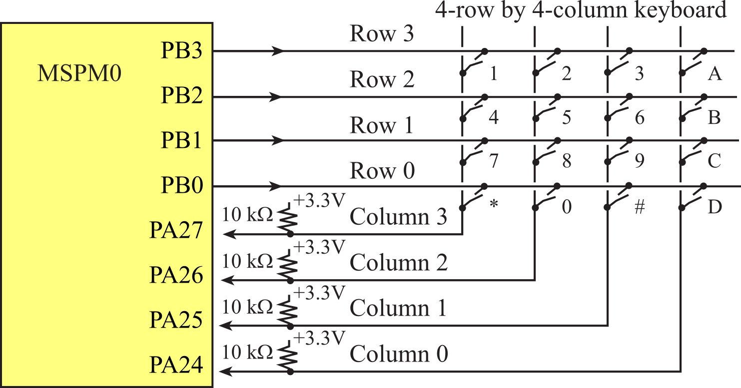
Figure M.1.2. A matrix keyboard interfaced to the microcontroller.
Program M.1.4 shows the initialization software. The data structure will assist in the scanning algorithm, and it provides a visual mapping from the physical layout of the keys to the ASCII code produced when touching that key. The structure also makes it easy to adapt this solution to other keyboard interfaces. A periodic interrupt can be used to debounce the switches. The key to debouncing is to not observe the switches more frequently than once every 10 ms.
void MatrixKeypad_Init(void){
IOMUX->SECCFG.PINCM[PB0INDEX] = 0x02000081; // HiZ GPIO output
IOMUX->SECCFG.PINCM[PB1INDEX] = 0x02000081; // HiZ GPIO output
IOMUX->SECCFG.PINCM[PB2INDEX] = 0x02000081; // HiZ GPIO output
IOMUX->SECCFG.PINCM[PB3INDEX] = 0x02000081; // HiZ GPIO output
GPIOB->DOE31_0 |= 0x0F; // enable output PB3,2,1,0
GPIOB->DOUTSET31_0 = 0x0F; // turn them all off
IOMUX->SECCFG.PINCM[PA27INDEX] = 0x00060081; // input, pull up
IOMUX->SECCFG.PINCM[PA26INDEX] = 0x00060081; // input, pull up
IOMUX->SECCFG.PINCM[PA25INDEX] = 0x00060081; // input, pull up
IOMUX->SECCFG.PINCM[PA24INDEX] = 0x00060081; // input, pull up
}
Program M.1.4. Initialization software for a matrix keyboard, assuming LaunchPad_Init has been called.
Program M.1.5 shows the
scanning software. The scanning sequence is listed in Table M.1.6. There are
two steps to scan a particular row:
- Select that row by driving it low, while the other rows are HiZ,
- Wait for the circuit to stabilize
- Read the columns to see if any keys are pressed in that row,
- 0 means the key is pressed
- 1 means the key is not pressed
It is important to observe column and row signals on a dual trace oscilloscope while running the software at full speed, because it takes time for correct signal to appear on the column after the row is changed. In most cases, a software delay should be inserted between setting the row and reading the column. The length of the delay you will need depends on the size of the pull-up resistor and any stray capacitance that may exist in your circuit.
|
Row |
PB0 |
PB1 |
PB2 |
PB3 |
PA24 |
PA25 |
PA26 |
PA27 |
|
0x01 |
0 |
HiZ |
HiZ |
HiZ |
1 |
2 |
3 |
A |
|
0x02 |
HiZ |
0 |
HiZ |
HiZ |
4 |
5 |
6 |
B |
|
0x04 |
HiZ |
HiZ |
0 |
HiZ |
7 |
8 |
9 |
C |
|
0x08 |
HiZ |
HiZ |
HiZ |
0 |
* |
0 |
# |
D |
Table M.1.6. Patterns for a 4 by 4 matrix keyboard.
struct Row{
uint32_t PinsToTurnOn; // output to select row
uint32_t PinsToTurnOff; // output to deselect row
char keycode[4];};
typedef const struct Row Row_t;
Row_t ScanTab[5]={
{ 0x01, 0x0E, "123A" }, // row 0
{ 0x02, 0x0D, "456B" }, // row 1
{ 0x04, 0x0B, "789C" }, // row 2
{ 0x08, 0x07, "*0#D" }, // row 3
{ 0x00, 0x00, " " }};
char MatrixKeypad_Scan(int32_t *Num){
Row_t *pt;
char column, key;
int32_t j;
(*Num) = 0;
key = 0; // default values
pt = &ScanTab[0];
while(pt->PinsToTurnOn){
GPIOB->DOUTSET31_0 = pt->PinsToTurnOff; // 3 pins are off output
GPIOB->DOUTCLR31_0 = pt->PinsToTurnOn; // one pin is on
Clock_Delay(24); // adjust this depending on capacitive load
column = ((GPIOA->DIN31_0&0x0F000000)>>24);// read columns
for(j=0; j<=3; j++){
if((column&0x01)==0){
key = pt->keycode[j];
(*Num)++;
}
column >>= 1; // shift into position
}
pt++;
}
return key;
}
// Waits for a key to be pressed, then released
// returns ASCII code for key pressed,
// n is the number of keys pressed
char MatrixKeypad_In(void){ int32_t n;
char letter;
do{
letter = MatrixKeypad_Scan(&n);
} while (n != 1); // repeat until exactly one
do{
letter = MatrixKeypad_Scan(&n);
} while (n != 0); // repeat until release
return letter;
}
Program M.1.5. Scanning software for a matrix keyboard
Two-key rollover occurs when the operator is typing quickly. For example, if the operator is typing the A, B, then C, he/she might type A, AB, B, BC, C, and then release. With rollover, the keyboard does not go through a no-key state in between typing. The hardware interface in Figure M.1.2 could handle two-key rollover, but the software solution in Program M.1.5 does not.
One of the problems with switches is called switch bounce. Many inexpensive switches will mechanically oscillate for up to a few milliseconds when touched or released. It behaves like an underdamped oscillator. These mechanical oscillations cause electrical oscillations such that a port pin will oscillate high/low during the bounce. In some cases, this bounce should be removed.
There are two good solutions to using interrupt synchronization for the keyboard. The approach implemented here uses periodic polling, because it affords a simple solution to both bouncing and two-key rollover. The time between interrupts is selected to be longer than the maximum bounce time, but shorter than the minimum time between key strikes. If you type ten characters per second, the minimum time between rising and falling edges is about 50 ms. Since switch bounce times are less than 10 ms, we will poll the keyboard every 25 ms. This means the average latency will be 12.5 ms, and the maximum latency will be 25 ms.
The initialization include GPIO, SysTick, and a FIFO. A key is recognized if the scanning returns one key found, and this key is different from what it scanned 25 ms ago.
#include "../inc/FIFO.h" // create a FIFO
char static LastKey;
uint32_t HeartBeat; // incremented every 25 ms
void Matrix_Init(void){
LastKey = 0; // no key
typed
HeartBeat = 0;
RxFifo_Init();
MatrixKeypad_Init();
SysTick_IntArm(Clock_Freq()/40,2); //40Hz, 25 ms polling
}
void SysTick_Handler(void){ char thisKey; int32_t n;
thisKey = MatrixKeypad_Scan(&n); // scan
if((thisKey != LastKey) && (n == 1)){
RxFifo_Put(thisKey);
LastKey = thisKey;
} else{
LastKey = 0; // invalid
}
HeartBeat++;
}
char Matrix_InChar(void){ char letter;
do{
letter = RxFifo_Get();
}while(letter == 0);
return(letter);
}
Program M.1.6. Periodic polling interface of a scanned keyboard.
One of the advantages of Program M.1.6 is two-key rollover. When people type very fast, they sometimes type the next key before the release the first key. For example, when the operator types the letters "BCD" slowly with one finger, the keyboard status goes in this sequence
<none>, <B>, <none>, <C>, <none>, <D>, <none>
Conversely, if the operator types quickly, there can be two-key rollover, which creates this sequence
<none>, <B>, <BC>, <C>, <CD>, <D>, <none>
where <BC> means both keys 'B' and 'C' are touched. Two-key rollover means the keyboard does not go through a state where no keys are touched between typing the 'B' and the 'C'. Since each of the keys goes through a state where exactly one key is pressed and is different than it was 25 ms ago, Program M.1.5 will handle two-key rollover.
A second approach is to arm the device for interrupts by driving all rows to zero. In this manner, we will receive a falling edge on one of the Port A inputs when any key is touched. During the ISR we could scan the keyboard and put the key into the FIFO. To solve the bounce problem this solution implements a time delay from key touch to when the software scans for keys. This approach uses a combination of edge-triggered inputs and timer interrupts to perform input in the background. When arming for interrupts, we set all four rows to output zero. In this way, a falling edge interrupt will occur on any key touched. When an edge-triggered interrupt occurs, we will disarm this input and arm an timer to trigger in 10 ms. It is during the timer ISR we scan the matrix. If there is exactly one key, we enter it into the FIFO. An interrupt may occur on release due to bounce. However, 10 ms after the release, when we scan during the timer ISR the MatrixKeypad_Scan function will return a Num of zero, and we will ignore it. This solution solves switch bounce, but not two-key rollover.
There are three solutions to debounce an individual switch
1) Blind synchronization: read switch, and then wait 10 ms
2) Periodic polling: use a periodic interrupt at 10 ms
3) Interrupt:
edge-triggered interrupt, then time delay interrupt
Two 12-bit ADCs are built into the MSPM0G3507 microcontroller, called ADC0 and ADC1. You will use the ADC to collect data. TExaSdisplay also uses the ADC to implement a voltmeter and oscilloscope. Table M.2.1 shows the ADC0 register bits required to perform sampling on a single channel. Any bits not specified will read 0. For a complete list of ADC registers, please refer to the MSPM0 technical reference manual. The value in the CLKCFG CLKFREQ and CTL0 will configure the conversion speed. We set bit 1 of CTL0 to enable conversions, and set bit 8 of CTL1 to start a conversion. CTL2 configures the ADC resolution and data format. MEMCTL[0] specifies which channel (pin) is the analog input. Table M.2.2 shows the mapping between pin and analog channel. Each ADC has 8 possible pins. We set SCOMP0 to 0 to specify 8 clocks periods to sample the analog input prior to conversion. Bit 0 of STATUS will be clear when the conversion is complete. Bits 11-0 of MEMRES[0] will contain the digital result of the conversion.
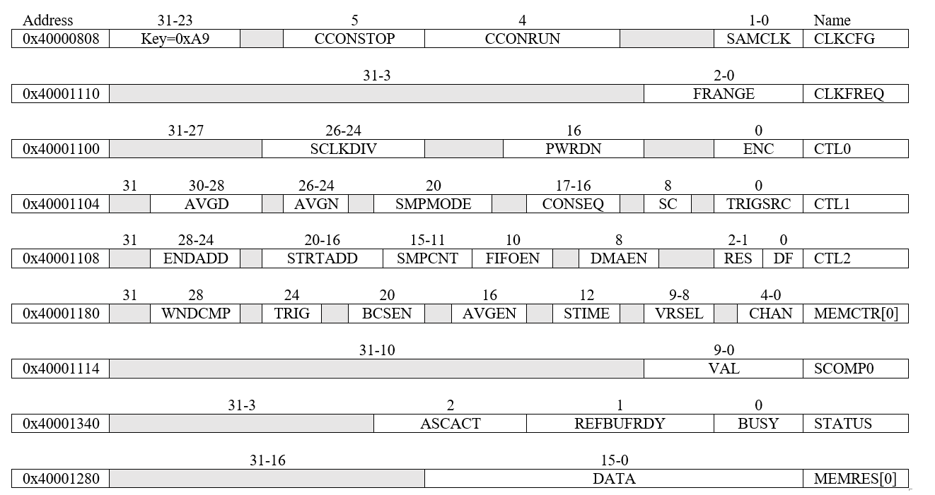
Table M.2.1. The MSM0 ADC registers. Each register is 32 bits wide.
|
Channel |
ADC0 pin |
ADC1 pin |
0 |
PA27 |
PA15 |
1 |
PA26 |
PA16 |
2 |
PA25 |
PA17 |
3 |
PA24 |
PA18 |
4 |
PB25 |
PB17 |
5 |
PB24 |
PB18 |
6 |
PB20 |
PB19 |
7 |
PA22 |
PA21 |
12 |
--- |
PA14 |
Table M.2.2. The MSPM0 has two ADCs, and 17 pins that can be used for analog to digital conversion.
Program M.2.1 configures the ADC for software start on one channel. Program M.2.1 shows a specific details for sampling PB20, which is channel 6 on ADC0. To use ADC1, simply change all the ADC0 to ADC1 in both Programs M.2.1 and M.2.2. To sample a different channel, edit step 9 to select the desired sample.
Step 1. We reset the ADC0 module.
Step 2. We activate the ADC0 module.
Step 3. We wait for 24 clocks for the ADC to stabilize.
Step 4. We connect the 40 MHz ULPCLK to the ADC
Step 5. We tell the ADC how fast the processor is running
Step 6. 40MHz/8 means the ADC is clocked at 5 MHz. ENC=0 means off.
Step 7. The mode is no averaging, software trigger, and one sample.
Step 8. CTR2 specifies the digital result is put in MEMRES.
Step 9. We select channel 6 with internal reference.
Step 10. We specify 8 clocks to observe the analog input before conversion.
Step 11. We disable interrupts on ADC.
Observation: The data sheet says the processor clock must be less than or equal to 40 MHz for the ADC to run. We have tested 100 boards so far and all boards allow the ADC to run with a processor clock of 80 MHz.
void ADC0_Init(void){
ADC0->ULLMEM.GPRCM.RSTCTL = 0xB1000003; // 1) reset
ADC0->ULLMEM.GPRCM.PWREN = 0x26000001; // 2) activate
Clock_Delay(24); // 3) wait
ADC0->ULLMEM.GPRCM.CLKCFG = 0xA9000000; // 4) ULPCLK
ADC0->ULLMEM.CLKFREQ = 7; // 5) 40-48 MHz
ADC0->ULLMEM.CTL0 = 0x03010000; // 6) divide by 8
ADC0->ULLMEM.CTL1 = 0x00000000; // 7) mode
ADC0->ULLMEM.CTL2 = 0x00000000; // 8) MEMRES
ADC0->ULLMEM.MEMCTL[0] = 6; // 9) channel 6 is PB20
ADC0->ULLMEM.SCOMP0 = 0; // 10) 8 sample clocks
ADC0->ULLMEM.CPU_INT.IMASK = 0; // 11) no interrupt
}
Program M.2.1. Initialization of the ADC0 channel 6, PB20, using software start, internal reference, and busy-wait.
: If the ADC is clocked at 5MHz, approximately how long does a 12-bit successive approximation conversion take?
Video M.2.1. ADC Initialization Ritual **needs recording
Program M.2.2 gives a function that performs an ADC conversion. There are five steps required to perform a software-start conversion. Let V be the analog input voltage in volts. Let data be the digital output of the ADC. The range is 0 to 3.3V. If the analog input is 0, the digital output will be 0, and if the analog input is 3.3V, the digital output will be 4095.
data = (V * 4095) / 3.3V
Step 1. Setting bit 0 of CTL0 enables the ADC.
Step 2. Setting bit 8 of CTL1 starts the ADC.
Step 3. A very short time delay is required for the busy bit to be correct.
Step 4. We wait for busy (bit 0 of CTL0) to be low (not busy).
Step 5. We read the 12-bit digital result.
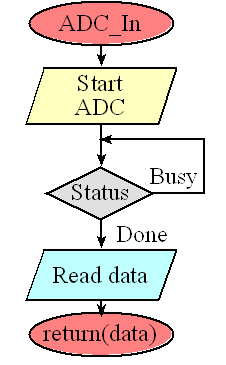
Figure M.2.3. The software uses busy-wait synchronization.
uint32_t ADC0_In(void){
ADC0->ULLMEM.CTL0 |= 0x00000001; // 1) enable conversions
ADC0->ULLMEM.CTL1 |= 0x00000100; // 2) start ADC
uint32_t volatile delay=ADC0->ULLMEM.STATUS; // 3) time to let ADC start
while((ADC0->ULLMEM.STATUS&0x01)==0x01){} // 4) wait for completion
return ADC0->ULLMEM.MEMRES[0]; // 5) 12-bit result
}
Program M.2.2. ADC sampling using software start and busy-wait.
Video M.2.2. Capturing a Sample **needs recording**
It is important to sample the ADC at a regular rate. One simple way to deploy periodic sampling is to perform the ADC conversion in a periodic ISR. In the following code, the sampling rate is determined by the rate of the periodic interrupt. The global variable, Flag is called a semaphore, which is set when new information is stored into the variable Data. We can connect PA0 to a logic analyzer or oscilloscope to verify the sampling rate. The triple toggle allows you to measure the time to execute the ISR and the time between interrupts.
uint32_t Data; // 0 to 4095
uint32_t Flag; // 1 means new data
void SysTick_Handler(void){
GPIOA->DOUTTGL31_0 = 0x01; // toggle PA0
GPIOA->DOUTTGL31_0 = 0x01; // toggle PA0
Data =
ADC0_In(); // Sample ADC
Flag =
1; //
Synchronize with other threads
GPIOA->DOUTTGL31_0 = 0x01; // toggle PA0
}
Program M.2.3. Real-time data acquisition system.
The main program will initialize Clock, LaunchPad, SysTick, ADC, and enable interrupts. In Figure M.2.4 configures SysTick to interrupt at 100 Hz. In the main loop, if the semaphore is set, the data is processed and the Flag is cleared. If the semaphore is not set, the main loop can perform other unrelated tasks.
int main(void){
__disable_irq();
LaunchPad_Init(); // resets and activates Port A and Port B
Clock_Init_HFXT_40_80MHz(0);
ADC0_Init();
SysTick_IntArm(800000,0); // Program 1.9.1, 80M/800000 = 100Hz
__enable_irq();
while(1){
if(Flag){
// process data
Flag = 0;
}
}
}
Program M.2.4. The main program to runs a real-time data acquisition system.
: If the input voltage is 1.65V, what value will the MSPM0 12-bit ADC return?
: If the input voltage is 1.0V, what value will the MSPM0 12-bit ADC return?
: What input voltage exists on the analog pin if the MSPM0 12-bit ADC returns a value of 1024?
: How would we change the above example to create a data acquistion system using PA15.
: If the bus clock is 80 MHz and we wish to sample at 10 Hz, what value do call SysTick_IntArm?
: If the bus clock is 80 MHz and the SysTick LOAD register is 79999, what will be the ADC sampling rate?
: Why did we set the SysTick priority to 0?
Observation: The triple toggle technique allows us to measure the execution time of the ISR (second to third toggle) and the time between interrupts (first toggle to the next first toggle).
Next, we will configure the ADC to sample a single channel at a periodic rate using a timer trigger. The most time-accurate sampling method is this timer-triggered sampling. There is virtually no sampling jitter because the hardware timer starts the ADC conversion. When the software runs the ISR does not affect when the data was sampled. It will be real time as long as the software runs the ISR before it is time to take the next sample. E.g., if the sampling rate is 1kHz, then the latency requirement of the software ISR is 1ms. Timer-triggered ADC sampling uses a publication/subscription (Pub-Sub) architecture. The timer publishes an event on Pub-Sub channel 1 periodically (TIMG0->FPUB_0 = 1, and the ADC subcribes to Pub-Sub channel 1 using it to start the ADC conversion (ADC0->ULLMEM.FSUB_0 = 0x00000001.
There are many steps to configure the ADC to sample a single channel at a periodic rate. The most accurate sampling method is timer-triggered sampling (EM3=0x5). On the TM4C123, the MUX fields are 4 bits wide, allowing us to specify channels 0 to 11. Timer-triggered sampling will have zero sampling jitter because the hardware starts each sample.
Step 1. Reset the ADC and Timer G0.
Step 2. Enable power to the ADC and Timer G0.
Step 3. Wait for the ADC and Timer G0 to power up.
Step 4. The sampling rate is specified by setting the timer clock, a divide by, a prescale and a reload register. In this case, the sampling rate is 40MHz/period/prescale.
Step 5. The periodic timer event (counter goes from 1 to 0) is published on Pub-Sub channel 1.
Step 6. The timer is configured to count down (from LOAD to 0), reloading automatically.
Step 7. The hardware trigger publication is enabled.
Step 8. The timer is enabled.
Step 9. Turn on the ADC clock.
Step 10. We set the assumption that the bus clock is 40-48MHz. However, the MSPM0 seems to run correctly with a bus clock of 80 MHz.
Step 11. The sampling mode is no shifting, no averaging, timer triggered, and stop on completion.
Step 12. The ADC on the MSPM0 has memory locations inside the device. Here, we set the start and stop address. Since there is one channel, the start and stop are the same.
Step 13. The MEMCTL[0] specifies which microcontroller pin will be sampled, see Table M.2.2.
Step 14. When the ADC converts runs the sample and hold, and then runs the successive approximation hardware 12 times. These settings determine how fast these two will occur. These can be increased to improve SNR but make the conversion slower.
Step 15. We subscribe the ADC to event channel 1. This is the hardware link between the Timer G0 and ADC0.
Step 16. Arming the ADC will trigger an interrupt on ADC completion.
Step 17. The ADC is started.
Step 18. The ADC interrupt is enabled in the NVIC.
Step 19. The priority is set. Even though sampling is a hard real-time task, the interrupt priority of the ADC need not be high, because at the time of the interrupt, the data is already sampled.
Step 20. After all configurations are set, we activate the timer.
The timer starts the conversion at a regular rate. Bit 8 (MEMRESIFLG0) in the ADC0->ULLMEM.CPU_INT.RIS register will be set when the conversion is done. This bit is armed and enabled for interrupting, so conversion complete will trigger an interrupt. The ISR acknowledges the interrupt by writing a 1 to ADC0->ULLMEM.CPU_INT.ICLRbit 8 (MEMRESIFLG0). The 12-bit result is read from the ADC0->ULLMEM.MEMRES[0]. Timer G0 runs in power domain PD0, so its clock is 40MHz. In order to reduce latency of other interrupt requests in the system, this ISR simply stores the 12-bit conversion in a FIFO, to be processed later in the main program. Program M.2.4 shows the initialization and interrupt service routine to affect the periodic sampling. To use a pin for ADC sampling, we assume its PINCM value is 0, disabling digital functionality.
void (*ADCTask)(uint32_t); // user function to be called when new ADC data ready
void ADC0_TimerG0_Init(uint32_t channel, uint16_t period, uint32_t prescale, uint32_t priority, void(*task)(uint32_t){
ADCTask = task; // hook to user code
ADC0->ULLMEM.GPRCM.RSTCTL = 0xB1000003; // step 1) Reset ADC and Timer G0
TIMG0->GPRCM.RSTCTL = 0xB1000003;
ADC0->ULLMEM.GPRCM.PWREN = 0x26000001; // step 2) Enable power ADC and Timer G0
TIMG0->GPRCM.PWREN = 0x26000001;
Clock_Delay(24); // step 3) wait for ADC G0 to power up
TIMG0->CLKSEL = 0x08; // step 4) set the sampling rate, use bus clock
TIMG0->CLKDIV = 0x00; // divide by 1
TIMG0->COMMONREGS.CPS = prescale-1; // divide by prescale,
TIMG0->COUNTERREGS.LOAD = period-1; // set reload register
TIMG0->FPUB_0 = 1; // step 5) publish on channel 1
TIMG0->COUNTERREGS.CTRCTL = 0x02; // step 6) Timer count down mode
TIMG0->GEN_EVENT0.IMASK = 1; // step 7) enable hardware event published on Chan1
TIMG0->COMMONREGS.CCLKCTL = 1; // step 8) turn on timer clock
ADC0->ULLMEM.GPRCM.CLKCFG = 0xA9000000; // step 9) turn on ADC clock ULPCLK
ADC0->ULLMEM.CLKFREQ = 7; // step 10) set sampling clock, assume bus is 40 to 48 MHz
ADC0->ULLMEM.CTL0 = 0x03010000; // divide by 8, power down on completion
ADC0->ULLMEM.CTL1 = 0x00000001; // step 11) set ADC sampling mode
// bits 30-28 =0 no shift
// bits 26-24 =0 no averaging
// bit 20 SAMPMODE=0 timer triggers
// bits 17-16 CONSEQ=01 ADC at start will be sampled once, 10 for repeated sampling
// bit 8 SC=0 for stop, =1 to software start
// bit 0 TRIGSRC=1 timer trigger
ADC0->ULLMEM.CTL2 = 0x00000000; // step 12) set memory address for samples
// bits 28-24 ENDADD (which MEMCTL to end)
// bits 20-16 STARTADD (which MEMCTL to start)
// bits 15-11 SAMPCNT (for DMA)
// bit 10 FIFOEN=0 disable FIFO
// bit 8 DMAEN=0 disable DMA
// bits 2-1 RES=0 for 12 bit (=1 for 10bit,=2for 8-bit)
// bit 0 DF=0 unsigned formant (1 for signed, left aligned)
ADC0->ULLMEM.MEMCTL[0] = channel; // step 13) set channel
// bit 28 WINCOMP=0 disable window comparator
// bit 24 TRIG trigger policy, =0 for auto next, =1 for next requires trigger
// bit 20 BCSEN=0 disable burn out current
// bit 16 = AVGEN =0 for no averaging
// bit 12 = STIME=0 for SCOMP0
// bits 9-8 VRSEL = 10 for internal VREF,(00 for VDDA)
// bits 4-0 channel = 0 to 7 and 12 are available
ADC0->ULLMEM.SCOMP0 = 0x64; // step 14) sample clocks
ADC0->ULLMEM.SCOMP1 = 0x32; // sample clocks
ADC0->ULLMEM.FSUB_0 = 0x00000001; // step 15) subscribe to chan 1
ADC0->ULLMEM.CPU_INT.IMASK = 0x00000100; // step 16) arm interrupt on MEMRESIFG0
ADC0->ULLMEM.CTL0 |= 1; // step 17) start
NVIC->ISER[0] = 1 << 4; // step 18) enable ADC0 interrupt
NVIC->IP[1] = (NVIC->IP[1]&(~0x000000FF))|(priority<<6); // step 19) set priority (bits 7,6) IRQ 4
TIMG0->COUNTERREGS.CTRCTL |= 0x01; // step 20) activate timer G0
}
void ADC0_IRQHandler(void){ uint32_t data; // 1000 Hz
ADC0->ULLMEM.CPU_INT.ICLR = 0x00000100;
data = ADC0->ULLMEM.MEMRES[0];
(*ADCTask)(data); // execute user task
ADC0->ULLMEM.CTL0 |= 1; // restart
}
Program M.2.4. Timer-triggered ADC sampling.
Program M.2.5 shows the high-level implementation of a real-time data acquisition system. Real-time sampling is implemented in the timer-triggered ADC sampling, and the processing occurs later in the main program. To get 10 Hz sampling, we set the prescale to 80, and the period to 50,000 (40MHz/80/50000 = 10Hz). As long as the average time to process a sample is less than 100ms, the FIFO size can be chosen so it never fills. Abstraction is the separation of what it does (Program M.2.5) from how it works (Program M.2.4).
void RealTimeTask(uint32_t data){
Debug_HeartBeat0(); // toggle LED
Fifo_Put(data);
}
int main(void){
__disable_irq();
Clock_Init_HFXT_40_80MHz(0); // 0.005% accurate running off external crystal oscillator
Debug_Init();
LaunchPad_Init();
Fifo_Init();
ADC0_TimerG0_Init(7,50000,80,1,&RealTimeTask);
__enable_irq();
while(1){uint32_t data;
while(Fifo_Get(&data)==0){}; // wait for data
Debug_HeartBeat1(); // toggle LED
// process data
}
}
}
Program M.2.5. High-level data acquisition.
: There are three variables called data in this code. Are they the same variable or different?
The ADC can handle a sequence of up to 23 samples. However ADC0 supports 8 pins and ADC1 supports 9 pins (see Table M.2.2). The basic idea of sampling multiple channels is to set the start and stop address in ULLMEM.CTL2 and then set each of the channels in ULLMEM.MEMCTL Program M.2.6 will sample any two ADC channels using busy-wait synchonization.
void ADC_InitDual(ADC12_Regs *adc12,uint32_t channel1,uint32_t channel2){
adc12->ULLMEM.GPRCM.RSTCTL = (uint32_t)0xB1000003;// Reset ADC
adc12->ULLMEM.GPRCM.PWREN = (uint32_t)0x26000001; // Enable power ADC)
Clock_Delay(24); // time for ADC to power up)
adc12->ULLMEM.GPRCM.CLKCFG = 0xA9000000; // ULPCLK)
adc12->ULLMEM.CLKFREQ = 7; // 40 to 48 MHz)
adc12->ULLMEM.CTL0 = 0x03010000;)
adc12->ULLMEM.CTL1 = 0x00010000; //software trigger)
adc12->ULLMEM.CTL2 = 0x02010000;)
// bits 28-24 ENDADD=2 (which MEMCTL to end))
// bits 20-16 STARTADD=1 (which MEMCTL to start))
// bits 15-11 SAMPCNT (for DMA))
// bit 10 FIFOEN=0 disable FIFO)
// bit 8 DMAEN=0 disable DMA)
// bits 2-1 RES=0 for 12 bit (=1 for 10bit,=2for 8-bit))
// bit 0 DF=0 unsigned formant (1 for signed, left aligned))
adc12->ULLMEM.MEMCTL[1] = channel1;)
adc12->ULLMEM.MEMCTL[2] = channel2;)
adc12->ULLMEM.SCOMP0 = 0; // 8 sample clocks)
adc12->ULLMEM.GEN_EVENT.IMASK = 0; // no interrupt)
}
void ADC_InDual(ADC12_Regs *adc12,uint32_t *d1, uint32_t *d2){){
adc12->ULLMEM.CTL0 |= 0x00000001; // enable conversions
adc12->ULLMEM.CTL1 |= 0x00000100; // start ADC
uint32_t volatile delay=adc12->ULLMEM.STATUS; // time to let ADC start
while((adc12->ULLMEM.STATUS&0x01)==0x01){}; // wait for completion
*d1 = adc12->ULLMEM.MEMRES[1];
*d2 = adc12->ULLMEM.MEMRES[2];
}
Program M.2.6. Software to sample two channels.
The MSPM0G3507 microcontroller has 7 timers, which can be used to create periodic interrupts. Timer G12 is a 32-bit hardware timer with no prescale; the other six are 16-bit timers with an 8-bit prescale. Each timer has a counter register, e.g., TIMG0->COUNTERREGS.CTR, which is incremented or decremented automatically in hardware. The 7 timers are listed in Table M.3.1. In periodic timer mode, the CTR register continuously counts down. Timers G0 and G8 are clocked at one half the bus frequency. Timers A0, A1, G6, G7, and G12 are clocked at the bus frequency. All timers except G12 have a clock prescale=CPS register containing an 8-bit prescale.
|
Load |
Prescale |
ULPCLK |
Power
Domain |
|
|
SysTick |
24 bit |
none |
80MHz |
|
|
TimerA0 |
16 bit |
8 bit |
80MHz |
PD1 |
|
TimerA1 |
16 bit |
8 bit |
80MHz |
PD1 |
|
TimerG0 |
16 bit |
8 bit |
40MHz |
PD0 |
|
TimerG12 |
32 bit |
none |
80MHz |
PD1 |
|
TimerG6 |
16 bit |
8 bit |
80MHz |
PD1 |
|
TimerG7 |
16 bit |
8 bit |
80MHz |
PD1 |
|
TimerG8 |
16 bit, |
8 bit |
40MHz |
PD0 |
Table M.3.1. Details on the 7 hardware timers.
If the bus clock period is Δt, then the timer counting period is
Δt*(CPS+1)*2 for G0 and G8
Δt*(CPS+1) for A0, A1, G6, G7, and G12
If we make the CPS=39 with a bus clock at 80 MHz, then Timer G0 counts down at 1 MHz (every 1us). Each timer also has a LOAD register, which is a 32-bit constant on G12 and 16-bit on the other six timers. When the timer counts from 1 to 0 it sets the trigger flag, which is bit 0 in the RIS register. On the next count, the CTR register is reloaded with the value in LOAD. In periodic mode, the CTR register continuously counts
LOAD, LOAD-1, LOAD-2,...2, 1, 0, LOAD, LOAD-1, LOAD-2,...
Therefore, the interrupt will occur every
Δt*(CPS+1)(LOAD+1)*2 for G0 and G8
Δt*(CPS+1)(LOAD+1) for A0, A1, G6, and G7
Δt*(LOAD+1) for G12
: Which timer would you use and how would you configure it to interrupt every 1 sec?
In periodic mode, the timer runs continuously. The timers can be used to create pulse width modulated outputs and measure pulse width, period, or frequency. Program M.3.1 shows the low-level driver using Timer G0 to trigger a periodic interrupt. With a bus clock of 80MHz, Timer G0 is clocked at 40MHz (25ns period). The slowest we could interrupt is if we set LOAD=0xFFFF and CPS=0xFF. At these settings, Timer G0 will interrupt every 25ns*256*65536 = 419.4304ms.
During initialization, we first reset and activate the timer. After a short delay, we set CLKSEL=0x08 and CLKDIV=0 to clock the timer from the bus clock. On G0 and G8 the timer will clock at 1/2 bus frequency. Next, we set the CPS and LOAD to specify the interrupt period. We set CTRCTL=0x02 to specify continuous down counting. We set bit 0 of IMASK to arm the periodic interrupt. We set bit 0 of CCLKCTL to enable the timer. Timer G0 is interrupt 16, so we enable Timer G0 interrupts by setting bit 16 in NVIC->ISER[0]. Remember NVIC->ISER[0] is a write 1 to set, but writing zeros has no effect on this register. Therefore, NVIC->ISER[0]=1<<16; is friendly. The priority bits for Timer G0 are bits 7-6 in NVIC->IP[4]. The last step is to enable the timer by setting bit 0 of CTRCTL.
The interrupt trigger flag is bit 0 of the RIS register. There are two ways the ISR can clear the trigger flag:
- Write 1 to the TIMG0->CPU_INT.ICR register
- Read the TIMG0->CPU_INT.IIDX register (which will return a 1)
Note also, TIMG0->CPU_INT.ICR is write 1 to clear, so,
TIMG0->CPU_INT.ICR=1; is also a friendly way clear bit 0 of RIS.
For a complete list of timer registers, please refer to the MSPM0 technical reference manual.
void (*PeriodicTask)(void); // user function
void TimerG0_IntArm(void(*task)(void), uint16_t period, uint32_t prescale, uint32_t priority){
TIMG0->GPRCM.RSTCTL = 0xB1000003;
TIMG0->GPRCM.PWREN = 0x26000001;
PeriodicTask = task; // user function
Clock_Delay(24); // time for TimerG0 to power up
TIMG0->CLKSEL = 0x08; // bus clock
TIMG0->CLKDIV = 0x00; // divide by 1
TIMG0->COMMONREGS.CPS = prescale-1; // divide by prescale,
TIMG0->COUNTERREGS.LOAD = period-1; // set reload register
TIMG0->COUNTERREGS.CTRCTL = 0x02;
// bits 5-4 CM =0, down
// bits 3-1 REPEAT =001, continue
// bit 0 EN enable (0 for disable, 1 for enable)
TIMG0->CPU_INT.IMASK = 1; // zero event mask
TIMG0->COMMONREGS.CCLKCTL = 1;
NVIC->ISER[0] = 1 << 16; // TIMG0 interrupt
NVIC->IP[4] = (NVIC->IP[4]&(~0x000000FF))|(priority<<6); // set priority (bits 7,6) IRQ 16
TIMG0->COUNTERREGS.CTRCTL |= 0x01;
}
void TIMG0_IRQHandler(void){
if((TIMG0->CPU_INT.IIDX) == 1){ // this will acknowledge
(*PeriodicTask)(); // execute user task
}
}
Program M.3.1. Periodic interrupts using Timer G0 .
Program M.3.2 shows the high-level driver usage, running b>myTask at 100 Hz. Abstraction is the separation of what it does (Program M.3.2) from how it works (Program M.3.1).
uint32_t count;
void MyTask(void){
GPIOB->DOUTTGL31_0 = GREEN; // toggle PB27
count++;
}
int main(void){
__disable_irq();
Clock_Init_HFXT_40_80MHz(0);
count=0;
LaunchPad_Init();
TimerG0_IntArm(&MyTask,10000,40,2); // 40MHz/40/10000 = 100Hz
__enable_irq();
while(1){
GPIOA->DOUTTGL31_0 = RED1;
}
}
Program M.3.2. Periodic interrupts using Timer G0 .
Video M.3.1. TimerG0 **needs recording**
Observation: If we set LOAD=0, the counter can never go from 1 to 0, so the interrupt flag will never be set. I.e., LOAD=0 is one way to halt the interrupts.
Program M.0.1 shows the interrupt vector table
Table M.0.1. shows the interrupt vectors
Table M.0.2 shows the priority registers and NVIC enable bits
: At what frequency will the heartbeat oscillate?
M.4.1. Registers
MSPM0 microcontrollers have four UARTs. The specific port pins used to implement the UARTs vary from one chip to the next. To find which pins your microcontroller uses, you will need to consult its datasheet. Table M.4.1 is a repeat of M.1.5 PINCM register for the MSPM0. Functionality UART1Rx means UART1 reciever pin (input), and UART1Tx means UART1 transmitter pin (output). Figure M.4.1 shows some of the UART registers. For a complete list, please refer to the MSPM0 technical reference manual.
Video M.4.1 UART initialization software
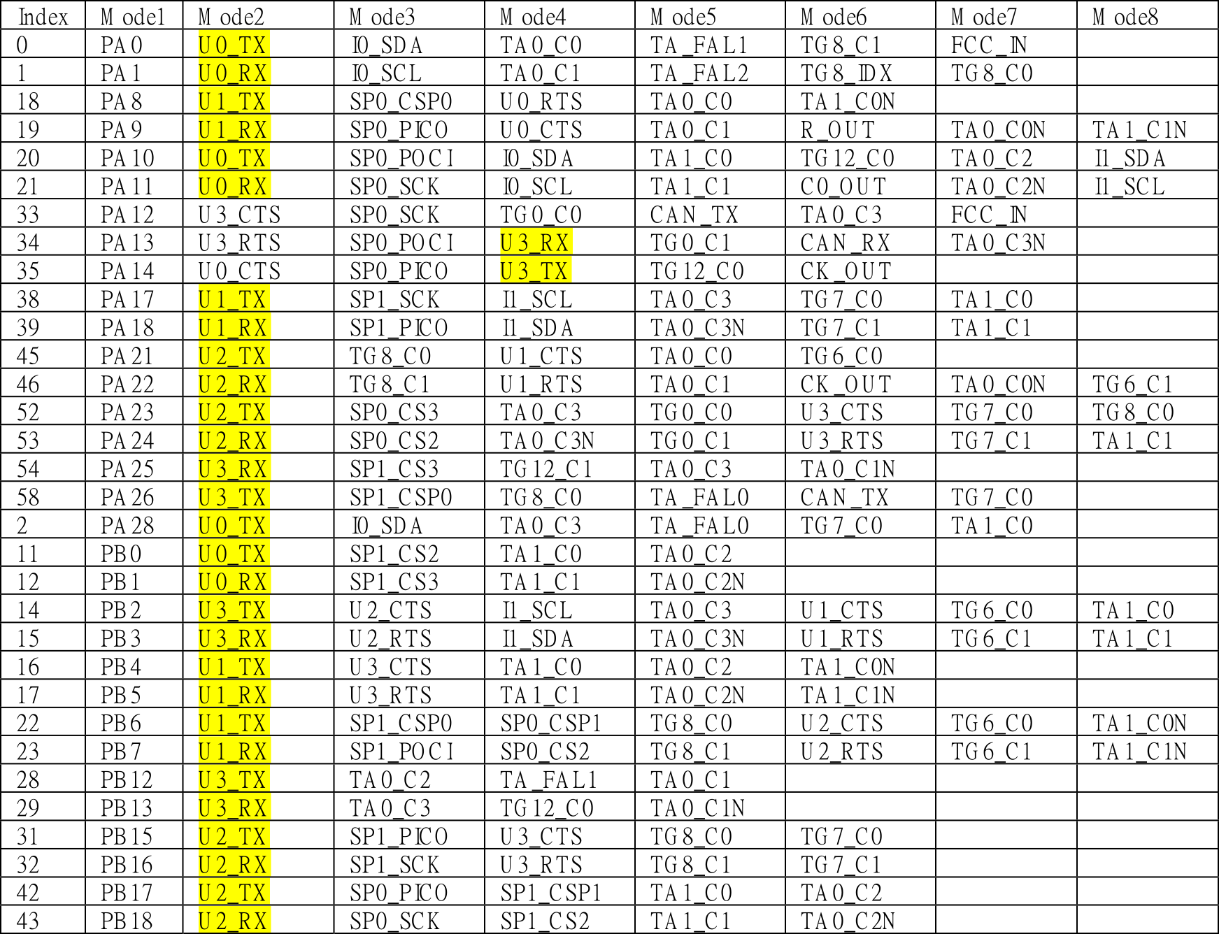
Table M.4.1. PINCM mode values needed for MSPM0 Pins. Entries highlighted in yellow can be used for UART.
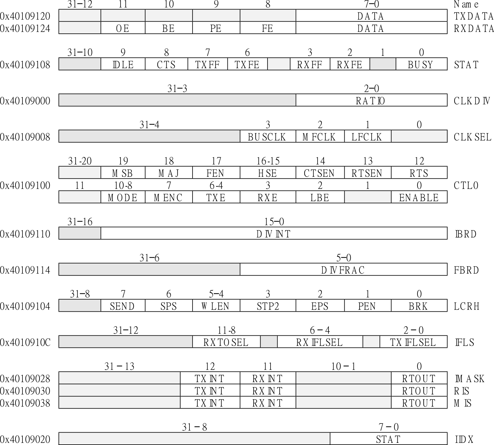
Figure M.4.1. MSPM0G3507 UART registers.
: Which pins can be used for UART2 transmitter?
: Which UART module do pins PB12/PB13 use?
M.4.2. Busy-wait UART1 Device Driver on PA10 and PA11
Software that sends and receives data must implement a mechanism to synchronize the software with the hardware. In particular, the software should read data from the input device only when data is indeed ready. Similarly, software should write data to an output device only when the device is ready to accept new data. With busy-wait synchronization, the software continuously checks the hardware status waiting for it to be ready. In this section, we will use busy-wait synchronization to write I/O programs that send and receive data using the UART. After a frame is received, the receive FIFO will be not empty (RXFE becomes 0) and the 8-bit data is available to be read. To get new data from the serial port, the software first waits for RXFE to be zero, then reads the result from UART0->RXDATA. Recall that when the software reads UART0->RXDATA it gets data from the receive FIFO. This operation is illustrated in Figure M.4.2 and shown in Program M.4.1. In a similar fashion, when the software wishes to output via the serial port, it first waits for TXFF to be clear, then performs the output. When the software writes UART0->TXDATA it puts data into the transmit FIFO.
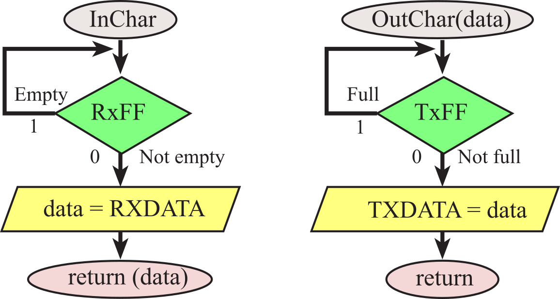
Figure M.4.2. UART Input/Output using busy-wait.
// Assumes a 80 MHz CPU clock, creates 115200 baud rate
void UART_Init(void){
UART0->GPRCM.RSTCTL = 0xB1000003; // reset UART0
UART0->GPRCM.PWREN = 0x26000001; // activate UART0
Clock_Delay(24); // time for uart to activate
// configure PA11 PA10 as alternate UART0 function
IOMUX->SECCFG.PINCM[PA10INDEX] = 0x00000082;
//bit 7 PC connected
//bits 5-0=2 for UART0_Tx
IOMUX->SECCFG.PINCM[PA11INDEX] = 0x00040082;
//bit 18 INENA input enable
//bit 7 PC connected
//bits 5-0=2 for UART0_Rx
UART0->CLKSEL = 0x08; // bus clock
UART0->CLKDIV = 0x00; // no divide
UART0->CTL0 &= ~0x01; // disable UART0
UART0->CTL0 = 0x00020018; // enable fifos, tx and rx
// 40000000/16 = 2,500,000, 2,500,000/115200 = 21.70139
UART0->IBRD = 21; // divider = 21+45/64 = 21.703125
UART0->FBRD = 45;
UART0->LCRH = 0x00000030; // 8bit, 1 stop, no parity
UART0->CTL0 |= 0x01; // enable UART0
}
char UART_InChar(void){
while((UART0->STAT&0x04) == 0x04){}; // wait while RxFifo empty
return((char)(UART0->RXDATA));
}
void UART_OutChar(char data){
while((UART0->STAT&0x80) == 0x80){}; // wait while TxFifo full
UART0->TXDATA = data;
}
Program M.4.1. Busy-wait solution for UART0
: Assume the bus clock is 80 MHz. What is the baud rate if UART0->IBRD equals 2 and UART0->FBRD equals 32?
: Assume the bus clock is 80 MHz. What values should you put in UART0->IBRD and UART0->FBRD to make a baud rate of 38400 bits/sec?
Video M.4.2. Change from PA10/PA11 to PB17/PB18, changing from UART0 to UART2.
: How does the software clear RXFE?
: How does the software clear TXFF?
: Describe what happens if the receiving computer is operating on a baud rate that is twice as fast as the transmitting computer?
: Describe what happens if the transmitting computer is operating on a baud rate that is twice as fast as the receiving computer?
M.4.3. Interrupting UART Device Driver
There are three fundamental aspects of serial communication common to all UARTs.
- Baud rate
- Format
- Hardware-software synchronization
Baud rate is the number of bits/sec. The baud rate is programmed into both the transmitter and receiver, and the rates should match within 5%. On the MSPM0, see the UART0->IBRD and UART0->FBRD registers.
The format defines the structure of the serial frame. There is always one start bit, but the number of data bits can vary. Most UARTs can add no, even, or odd parity. Many UARTs can operate with 1 or 2 stop bits. Just like baud rate, the format is programmed into both the transmitter and receiver, and the formats must match. See the the UART0->LCRH register.
We could use busy-wait or interrupt synchrononization. Different from baud rate and format, the tranmitter and receiver do not need to use the same synchronization. For efficient performance, we will use busy-wait only when we know the software will never wait. For example, if the size of the tranmitted message is less than the size of the hardware TxFifo, and the rate of sending message allows the previous message to be completely sent before the next message is attempted, then busy-wait in the transmitter is allowed because it will never wait. Often this timing cannot be guaranteed, so interrupts are needed. To use interrupts we will enable the FIFOs by setting the FEN bit in the UART0->LCRH register. RXIFLSEL specifies the receive FIFO level that causes an interrupt.
RXIFLSEL
Set RXRIS interrupt trigger when
0x1 RXFIFO ≥ 1/4 full
0x2 RXFIFO ≥ 1/2 full
0x3 RXFIFO ≥ 3/4 full
0x4 RXFIFO is full
TXIFLSEL specifies the transmit FIFO level that causes an
interrupt.
TXIFLSEL
Set TXRIS
interrupt trigger when
0x1 TXFIFO ≤ 3/4 empty
0x2 TXFIFO ≤ 1/2 empty
0x3 TXFIFO ≤ 1/4 empty
0x4 TXFIFO is empty
The register UART0->IMASK contains the ARM
bits.
Bit 0 RTIM arm receiver timeout
Bit 11 TXIM arm transmit FIFO (see TXIFLSEL)
Bit 10 RXIM arm receive FIFO (see RXIFLSEL)
The register UART0_RIS_R contains the trigger flag (set by
hardware on UART event).
Bit 0 RTRIS trigger flag for receiver timeout
Bit 11 TXRIS trigger flag for transmit FIFO (see
TXIFLSEL)
Bit 10 RXRIS trigger flag for receive FIFO (see
RXIFLSEL)
The register UART0->ICR contains the acknowledge bits
(software writes 1 to clear trigger flag).
Bit 0 RTIC acknowledge receiver timeout
Bit 11 TXIC acknowledge transmit FIFO (see TXIFLSEL)
Bit 10 RXIC acknowledge receive FIFO (see RXIFLSEL)
Figure M.4.3 shows a data flow graph with buffered input and buffered output. FIFOs used in this book will be statically allocated global structures. Because they are global variables, it means they will exist permanently and can be carefully shared by more than one program. The advantage of using a FIFO structure for a data flow problem is that we can decouple the producer and consumer threads. Without the FIFO we would have to produce one piece of data, then process it, produce another piece of data, then process it. With the FIFO, the producer thread can continue to produce data without having to wait for the consumer to finish processing the previous data. This decoupling can significantly improve system performance.

Figure M.4.3. A data flow graph showing two FIFOs that buffer data between producers and consumers.
The flowchart for using two FIFOs is illustrated in Figure M.4.4. With mailbox synchronization, the threads execute in lock-step: one, the other, one, the other… However, with the FIFO queue execution of the threads is more loosely coupled. The classic producer/consumer problem has two threads. One thread produces data and the other consumes data. For an input device, the background thread is the producer because it generates new data, and the foreground thread is the consumer because it uses the data up. For an output device, the data flows in the other direction so the producer/consumer roles are reversed. It is appropriate to pass data from the producer thread to the consumer thread using a FIFO queue

Figure M.4.4. In a producer/consumer system, FIFO queues can be used to pass data between threads.
void UART_Init(void){
UART0->GPRCM.RSTCTL = 0xB1000003;
UART0->GPRCM.PWREN = 0x26000001;
Clock_Delay(24); // time for uart to power up
// configure PA11 PA10 as alternate UART0 function
IOMUX->SECCFG.PINCM[PA10INDEX] = 0x00000082;
//bit 7 PC connected
//bits 5-0=2 for UART0_Tx
IOMUX->SECCFG.PINCM[PA11INDEX] = 0x00040082;
//bit 18 INENA input enable
//bit 7 PC connected
//bits 5-0=2 for UART0_Rx
TxFifo_Init();
RxFifo_Init();
UART0->CLKSEL = 0x08; // bus clock
UART0->CLKDIV = 0x00; // no divide
UART0->CTL0 &= ~0x01; // disable UART0
UART0->CTL0 = 0x00020018;
// bit 17 FEN=1 enable FIFO
// bits 16-15 HSE=00 16x oversampling
// bit 14 CTSEN=0 no CTS hardware
// bit 13 RTSEN=0 no RTS hardware
// bit 12 RTS=0 not RTS
// bits 10-8 MODE=000 normal
// bits 6-4 TXE=001 enable TxD
// bit 3 RXE=1 enable TxD
// bit 2 LBE=0 no loop back
// bit 0 ENABLE 0 is disable, 1 to enable
// 40000000/16 = 2,500,000 Hz
// Baud = 115200
// 2,500,000/115200 = 21.701388
// divider = 21+45/64 = 21.703125
UART0->IBRD = 21;
UART0->FBRD = 45; // baud =2,500,000/21.703125 = 115,191
UART0->LCRH = 0x00000030;
// bits 5-4 WLEN=11 8 bits
// bit 3 STP2=0 1 stop
// bit 2 EPS=0 parity select
// bit 1 PEN=0 no parity
// bit 0 BRK=0 no break
UART0->CPU_INT.IMASK = 0x0C01;
// bit 11 TXINT
// bit 10 RXINT
// bit 0 Receive timeout
UART0->IFLS = 0x0422;
// bits 11-8 RXTOSEL receiver timeout select 4 (0xF highest)
// bits 6-4 RXIFLSEL 2 is greater than or equal to half
// bits 2-0 TXIFLSEL 2 is less than or equal to half
NVIC->ICPR[0] = 1<<15; // UART0 is IRQ 15
NVIC->ISER[0] = 1<<15;
NVIC->IP[3] = (NVIC->IP[3]&(~0xFF000000))|(2<<30); // set priority (bits 31,30) IRQ 15
UART0->CTL0 |= 0x01; // enable UART0
}
// copy from hardware RX FIFO to software RX FIFO
// stop when hardware RX FIFO is empty or software RX FIFO is full
void static copyHardwareToSoftware(void){char letter;
while(((UART0->STAT&0x04) == 0) && (RxFifo_Size() < (RXFIFOSIZE - 1))){
letter = UART0->RXDATA;
RxFifo_Put(letter);
}
}
char UART_InChar(void){char letter;
do{
letter = RxFifo_Get();
}while(letter==0);
return(letter);
}
// copy from software TX FIFO to hardware TX FIFO
// stop when software TX FIFO is empty or hardware TX FIFO is full
void static copySoftwareToHardware(void){char letter;
while(((UART0->STAT&0x80) == 0) && (TxFifo_Size() > 0)){
letter = TxFifo_Get();
UART0->TXDATA = letter;
}
}
void UART_OutChar(char data){
while(TxFifo_Put(data) == 0){};
UART0->CPU_INT.IMASK &= ~0x0800; // disarm TX FIFO interrupt
copySoftwareToHardware();
UART0->CPU_INT.IMASK |= 0x0800; // rearm TX FIFO interrupt
}
void UART0_IRQHandler(void){ uint32_t status;
status = UART0->CPU_INT.IIDX; // reading clears bit in RIS
if(status == 0x01){ // 0x01 receive timeout
copyHardwareToSoftware();
}else if(status == 0x0B){ // 0x0B receive
copyHardwareToSoftware();
}else if(status == 0x0C){ // 0x0C transmit
copySoftwareToHardware();
if(TxFifo_Size() == 0){ // software TX FIFO is empty
UART0->CPU_INT.IMASK &= ~0x0800; // disable TX FIFO interrupt
}
}
}
Program M.4.2. Interrupting solution for UART0.
Details of the NVIC interrupts can be found back in Section
M.0. Refer to Section M.0 to answer these next three
checkpoints:
: At what address is the UART2_Handler ISR vector?
: How do you arm UART2_Handler ISR in the NVIC?
: Where are the priority bits for the UART2 interrupt 14?
Figure M.4.5 shows a data flow graph of an interrupting serial port from Lab 8 in Volume 1. Because the signals are encoded as voltages, the grounds must connected together. Figure M.4.5 is classified as full-duplex, because transmission can occur in both directions simultaneously.
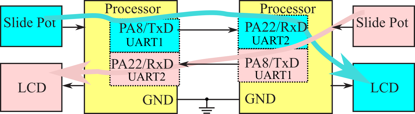
Figure M.4.5. Full-duplex serial
communication channel (ECE419K Lab 8).
M.5. Synchronous Transmission and Receiving using the SPI
M.5.1. Details on the MSPM0
Serial Peripheral Interface (SPI) is a synchronous serial protocol. Serial means data is transmited on a single line, one bit at a time. Synchronous means the protocol also includes a clock, see SCK in Figure M.5.1. In its simplest form, SPI connects one controller (also called master) to one peripheral (also called slave). PICO (peripheral in controller out) is a serial line transmitting data from controller to peripheral. Another name for PICO is master out slave in (MOSI). Data can flow in both directions at the same time (called full duplex). POCI (peripheral out controller in) is a serial line transmitting data from peripheral to controller. Another name for POCI is master in slave out (MISO). The SPI protocol also includes a chip select (CS), which is driven low by the controller during a transmission. The peripheral will interact with a transmission if its chip select is low. Chip select is negative logic, meaning the inactive state is high, and the active state is low.
The SPI system can operate as a master or as a slave. The channel can have one master and one slave (left side of Figure M.5.1), or it can have one master and multiple slaves (right side of Figure M.5.1). With the ST7735 from Adafruit or HiLetGo, we will need to implement a multiple slave configuration because SPI1 is shared with the ST7735 LCD and the secure digital card. The master initiates all data communication.
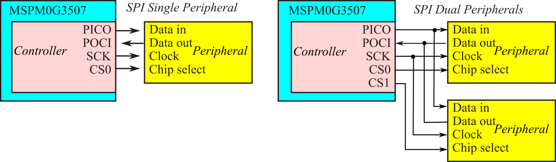
Figure M.5.1. The four signals that comprise SPI.
Observation: Compare the one-master/one-slave configuration in ST7735.c to the multiple-slave configuration in ST7735_SDC.c.
The MSPM0G3507 has two SPI modules. The fundamental difference between a UART, which implements an asynchronous protocol, and a SPI, which implements a synchronous protocol, is the manner in which the clock is implemented. Two devices communicating with asynchronous serial interfaces (UART) operate at the same frequency (baud rate) but have separate hardware to create their clocks. With a UART protocol, the clock signal is not included in the interface cable between devices. Two UART devices can communicate with each other as long as the two clocks have frequencies within ±5% of each other. Two devices communicating with synchronous serial interfaces (SPI) operate from the same hardware clock (synchronized). With a SPI protocol, the clock signal is included in the interface cable
Table M.5.1 lists the available pins for each SPI function.
|
Function |
Pin |
Pin |
Pin |
Pin |
|
SPI0_PICO |
PA9 (3) |
PA14 (3) |
PB17 (3) |
|
|
SPI0_POCI |
PA10 (3) |
PA13 (3) |
PB19 (3) |
|
|
SPI0_SCK |
PA11 (3) |
PA12 (3) |
PB18 (3) |
|
|
SPI0_CS0 |
PA2 (3) |
PA8 (3) |
PB25 (3) |
|
|
SPI0_CS1 |
PB6 (4) |
PB24 (3) |
PB26 (3) |
|
|
SPI0_CS2 |
PA24 (3) |
PB7 (4) |
PB20 (2) |
|
|
SPI0_CS3 |
PA23 (3) |
PA14 (4) |
PB24 (2) |
|
|
SPI1_PICO |
PA18 (3) |
PB8 (3) |
PB15 (3) |
PB22 (2) |
|
SPI1_POCI |
PA16 (3) |
PB7 (3) |
PB14 (3) |
PB21 (2) |
|
SPI1_SCK |
PA17 (3) |
PB9 (3) |
PB18 (3) |
PB23 (2) |
|
SPI1_CS0 |
PA26 (3) |
PB6 (3) |
PB20 (3) |
|
|
SPI1_CS1 |
PA27 (3) |
PB17 (4) |
PB27
(3) |
|
|
SPI1_CS2 |
PA15 (3) |
PB0 (3) |
PB18 (4) |
|
|
SPI1_CS3 |
PA25 (3) |
PB1 (3) |
PB14 (2) |
|
Table M.5.1. SPI pin options (PF=digital Mode), see also the PINCM register.
One edge of the clock is used by the transmitter to change the data, and the other edge of the clock is used by the receiver to read the data. This way the data is stable when the receiver reads it. In Figure M.5.2, T marks the time the controller changes the output pin. The DA interval shows when the data output (PICO) is available or valid. R marks the time the peripheral reads the pin. The time period prior to R when the receiver is preparing to read is the setup time. The time period after R that the receiver expects the incoming data to be hold is called the hold time. The DR interval shows when the data is required to be valid. To operate correctly, the DA interval must overlap (start before and end after) the DR interval.
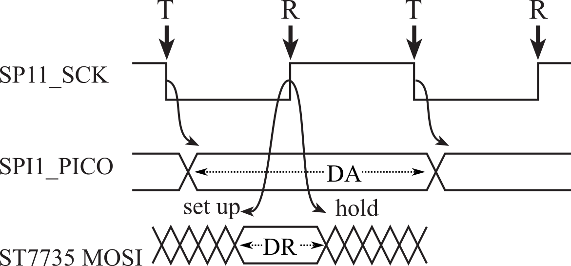
Figure M.5.2. Data output and data input are synchronized to the clock.
Observation Synchronous protocols are fast and reliable.
: In Figure M.5.2, the rising edge of the clock stores PICO into the peripheral. What is the definition of set up time?
: What is the definition of hold time?
: Define the data required interval in terms of the clocking edge, the set up time, and the hold time.
The SPI protocol sends 4 to 16 bits in a transmission. The interface to the ST7735R display utilizes an 8-bit frame, see Figure M.5.3. The CS goes low, 8 bits are transmitted synchronized to 8 pulses on SCK, and then CS goes high.
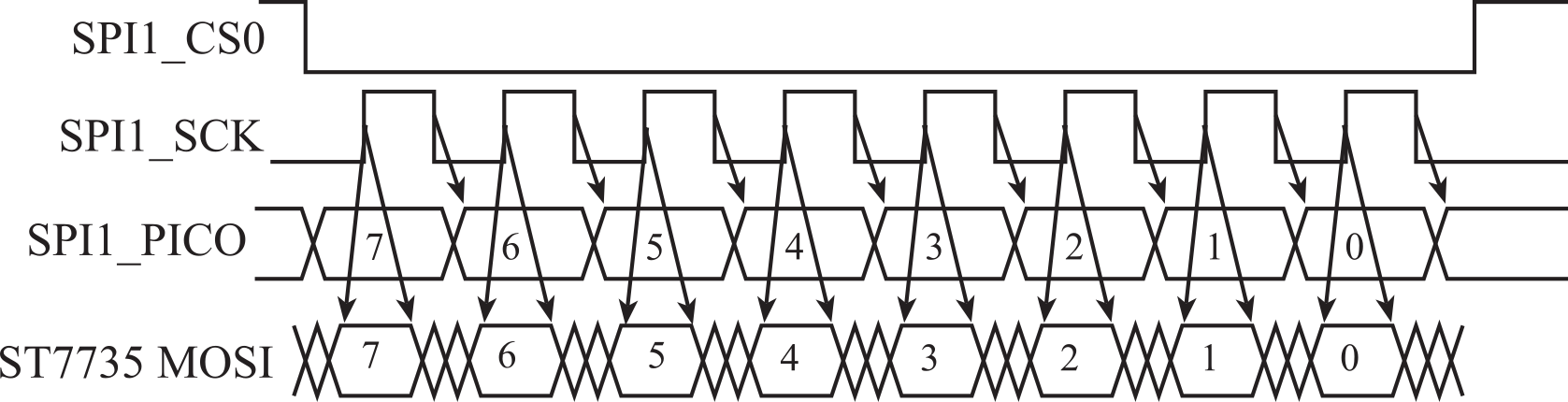
Figure M.5.3. One frame transmits 8 bits of data.
: What is the order of the bits sent serially with SPI?
The SPI transmits data at the same time as it receives input. The SPI changes its output on the opposite edge of the clock as it uses to shift data in. There are three mode control bits (CP, SPO, SPH) that affect the transmission protocol. If the device is a master (CP=0) it generates the SCLK, and data is output on the PICO pin, and input on the POCI pin. The SPO control bit specifies the polarity of the SCLK. In particular, the SPO bit specifies the logic level of the clock when data is not being transferred. The SPH bit affects the timing of the first bit transferred and received. If SPH is 0, then the device will shift data in on the first (and 3rd, 5th, 7th, … etc.) clock edge. If SPH is 1, then the device will shift data in on the second (and 4th, 6th, 8th, … etc.) clock edge. The data is transmitted MSB first is the MSB bit is 1. The four modes are shown in Figure M.5.4.
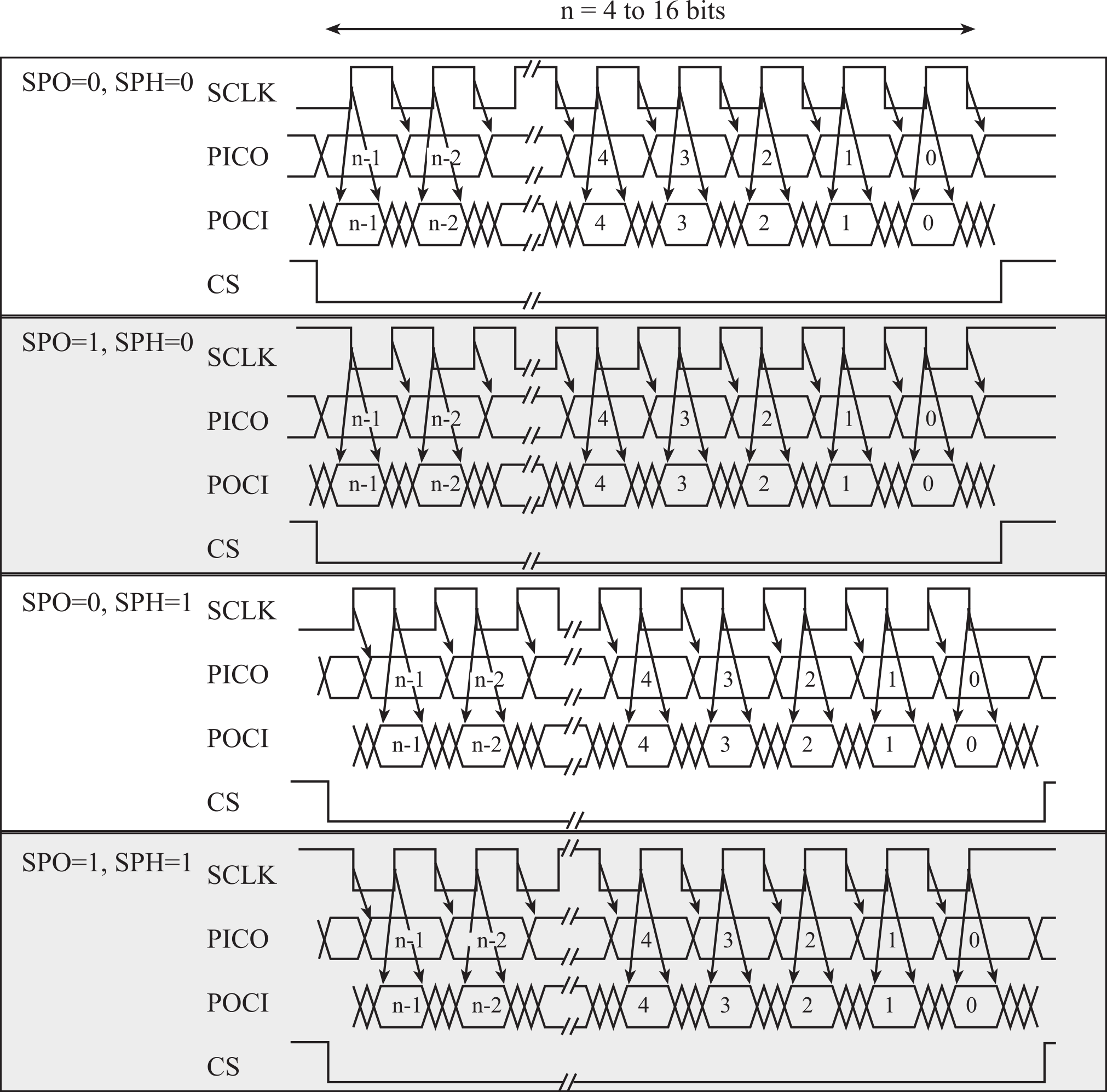
Figure M.5.4. One frame transmits 8 bits of data.
The SPI protocol bidirectional transmission. We classify it as full duplex because data flows in both directions at the same time. The SPI interface supported two shift registers, one in the controller and a second in the peripheral. Both shift registers are clocked at the same time, using one edge to shift the data out and the other edge to shift the data in, see Figure M.5.5.
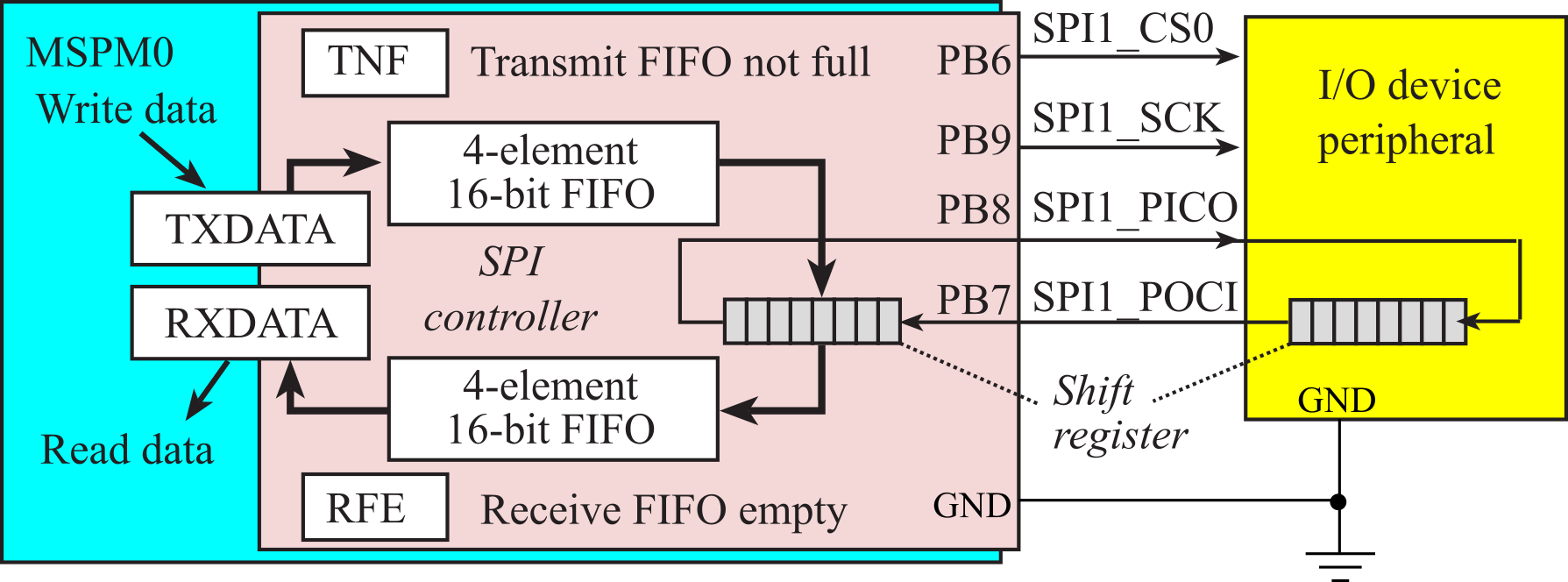
Figure M.5.5. The SPI protocol exchanges the data in the two shift registers.
: Explain how SPI is full duplex?
: What makes this protocol both fast and reliable?
Table M.5.2 lists some of the
SPI1 registers on the MSPM0G3507. In this section, we will focus on the data transfer
using busy-wait synchronization. The
RFE bit will be 1 if the SPI receive fifo is empty. The busy-wait input code can spin
on this status bit when inputing from the peripheral. The
TNF bit will be 1 if the SPI transmit fifo is not full. The busy-wait output code can spin
on this status bit when outputing to the peripheral.
If the interface sends one byte at time, we can spin on the TFE bit, which will be 1 if the SPI transmit fifo is empty.
The
BSY bit will be 1 if there is any tranmission in progress. The ST7735 interface uses this bit to make sure
the interface is completely idle before starting another communication.
|
Address |
31-16 |
15-0 |
|
||||||
|
0x4046B140 |
|
Data |
SPI1->TXDATA |
||||||
|
0x4046B130 |
|
Data |
SPI1->RXDATA |
||||||
|
|
|
|
|
|
|
|
|
|
|
|
Address |
9 |
8 |
- |
4 |
3 |
2 |
1 |
0 |
|
|
0x4046B110 |
|
|
|
BSY |
RNF |
RFE |
TNF |
TFE |
SPI1->STAT |
|
0x4046B100 |
SPH |
SPO |
|
DSS |
SPI1->CTL0 |
||||
|
0x4046B104 |
|
PREN |
|
MSB |
POD |
CP |
LBM |
ENABLE |
SPI1->CTL1 |
Table M.5.2. Some MSPM0G3507 SPI1 registers. Each
register is 32 bits wide.
M.5.2. MAX5353 DAC example
This example shows a synchronous serial interface between the microcontroller and a Maxim MAX5353 12-bit digital to analog converter as drawn in Figure M.5.6. A digital to analog converter (DAC) accepts a digital input (in our case a number between 0 and 4095) and creates an analog output (in our case a voltage between 0 and VREF*GAIN.) Discussion of DACs is presented in Section 5.2. Here in this section, we will focus on the digital hardware and software aspects of the serial interface.
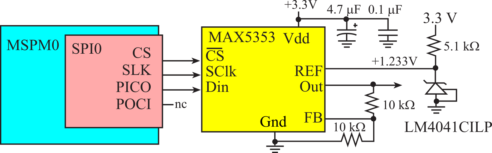
Figure M.5.6. A 12-bit DAC interfaced to the SPI port.
Table M.5.3 and Figure M.5.7 describe the protocol. The first 3 bits sent will be zero, then the 12 data bits that specify the analog output, and then one more zero will be sent. The CS control signal will be low during the 16-bit transmission. As with any SPI interface, there are basic interfacing issues to consider.
Word size. In this case we need to transmit 16 bits to the DAC. The MAX5353 data sheet specifies that the first three bits are command codes, the next 12 bits are the DAC output (MSB transmitted first), and the last bit is zero. Bit order. The MAX5353 requires the most significant bits first.
Clock phase, clock polarity. There are two issues to resolve. Since the MAX5353 samples its serial input data on the rising edge of the clock, the SPI must change the data on the falling edge. SPO=SPH=0 (Figure M.5.4) and SPO=SPH=1 both satisfy this requirement. The second issue is which edge comes first the rise or the fall. In this interface it probably doesn't matter.
Bandwidth. We look at the timing specifications of the MAX5353. The minimum clock low width of 40 ns means the shortest SPI period we can use is 100 ns. The commands are:
|
C2 |
C1 |
C0 |
D11 : D0 MSB LSB |
S0 |
Description |
|
X |
0 |
0 |
12 bits of data |
0 |
Load input register; DAC register immediately updated. |
|
X |
0 |
1 |
12 bits of data |
0 |
Load input register; DAC register unchanged. |
|
X |
1 |
0 |
XXXXXXXXXXXX |
X |
Update DAC register from input register. |
|
1 |
1 |
1 |
XXXXXXXXXXXX |
X |
Shutdown |
|
0 |
1 |
1 |
XXXXXXXXXXXX |
X |
No operation |
Table M.5.3. MAX5353 protocols
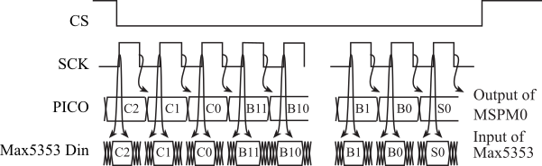
Figure M.5.7. MAX5353 DAC serial timing.
The ritual initializes the
Freescale SPI master mode, 16-bit data, and 8 MHz bandwidth. To
change the DAC output, one 16-bit transmission is
sent (DAC_Out).
The data returned in this case is not significant because the
DAC does not return data, so the POCI pin in
Figure M.5.6 is left not connected. In this example, the bus clock is 80 MHz,
and the SPI clock will be 8 MHz. Both SPI0 and SPI1 are in power domain PD1, sso SYSCLK equals bus CPU clock,
which is 80 MHz in this example. The SPI baud rate depends on the bus clock and the SCR value,
which we will set to 4:
SPI baud rate = SYSCLK / ((1 + SCR) * 2)
void DAC_Init(uint16_t data){
// assumes GPIOA and GPIOB are reset and powered previously
SPI0->GPRCM.RSTCTL = 0xB1000003;
SPI0->GPRCM.PWREN = 0x26000001;
// configure PB18 PB17 PA8 as alternate SPI0 function
IOMUX->SECCFG.PINCM[PB18INDEX] = 0x00000083; // SPI0 SCLK
IOMUX->SECCFG.PINCM[PA8INDEX] = 0x00000083; // SPI0 CS0
IOMUX->SECCFG.PINCM[PB17INDEX] = 0x00000083; // SPI0 PICO
Clock_Delay(24); // time for gpio to power up
SPI0->CLKSEL = 8; // SYSCLK
SPI0->CLKDIV = 0; // divide by 1
// SCR is in bits 2-0 (0 to 7), divide by SCR+1
SPI0->CLKCTL = 4; // 8 MHz = 80MHz/((4 + 1) * 2)
SPI0->CTL0 = 0x002F;
// bit 14 CSCLR=0 not cleared
// bits 13-12 CSSEL=0 CS0
// bit 9 SPH = 0
// bit 8 SPO = 0
// bits 6-5 FRF = 01 (4 wire)
// bits 4-0 n=15, data size is n+1 (16-bit data)
SPI0->CTL1 = 0x0015;
// bits 29-24 RXTIMEOUT=0
// bits 23-16 REPEATX=0 disabled
// bits 15-12 CDMODE=0 manual
// bit 11 CDENABLE=0 CS3
// bit 7-5 =0 no parity
// bit 4=1 MSB first
// bit 3=0 POD (not used, not peripheral)
// bit 2=1 CP controller mode
// bit 1=0 LBM disable loop back
// bit 0=1 enable SPI
}
void DAC_Out(uint16_t code){
while((SPI0->STAT&0x02) == 0x00){}; // spin if TxFifo full
SPI0->TXDATA = data;
}
Program M.5.1. Functions to initialize and to send data to the MAX5353 DAC using the SPI.
: How would you change Program M.5.1 to run at 10 MHz, assuming the bus frequency is 80 MHz?
M.5.3. ADXL362 accelerometer example
This second SPI example shows a synchronous serial interface between the computer and an ADXL362 3-axis MEMS Accelerometer, which measures acceleration in three dimensions. The ADXL345 is similar device, but uses SPO=1, SPH=1 mode. Here in this section we will focus on the hardware and software aspects of the serial interface (Figure M.5.8). Again, the basic interfacing issues to consider for this interface are:
Word size. To write a command we need to transmit 24 bits to the ADXL362. To read a result, we first transmit 16 bits and then we receive 8 bits. The software will implement 8-bit transmissions with the SPI module.
Bit order. The ADXL362 requires the most significant bits first.
Clock phase, clock polarity. Since the ADXL362 samples its serial input data on the rising edge of the clock, the SPI must changes the data on the falling edge. SPO=SPH=0 and SPO=SPH=1 both satisfy this requirement. We will use the SPO=SPH=0 mode as suggested in the Analog Devices data sheet, refer back to Figure M.5.4.
Bandwidth. We look at the timing specifications of the ADXL362. The maximum SCLK frequency is 8 MHz, and the minimum clock low/high widths is 50 ns, so the shortest SPI period we can use is 125ns.

Figure M.5.8. A three-axis accelerometer interfaced to the SPI port.
The first 8 bits sent will specify read (0x0B) or write (0x0A) as shown in Figure M.5.9. The second 8 bits will specify the register from which to read, or to which to write. On a read operation the last 8 bits will be the value returned from the ADXL362 to the microcontroller. On a write operation, the last 8 bits will be the value written from the microcontroller to the ADXL362. Because we want the CS signal to remain low for the entire 24-bit transfer, we will implement it using the regular I/O pin functions.

Figure M.5.9. ADXL362 serial timing.
Recall that when the software outputs to the SPI data register, the 8-bit register in the SPI is exchanged with the 8-bit register in the ADXL362. To communicate with the ADXL362, three 8-bit transmissions are exchanged.
void ADXL362_Init(void){
// assumes GPIOA and GPIOB are reset and powered previously
SPI0->GPRCM.RSTCTL = 0xB1000003;
SPI0->GPRCM.PWREN = 0x26000001;
IOMUX->SECCFG.PINCM[PB4INDEX] = 0x00000081; // GPIO output
GPIOB->DOE31_0 |= 1<<4;
// configure PB19 PB18 PB17 PA8 as alternate SPI0 function
IOMUX->SECCFG.PINCM[PB18INDEX] = 0x00000083; // SPI0 SCLK
IOMUX->SECCFG.PINCM[PA8INDEX] = 0x00000083; // SPI0 CS0
IOMUX->SECCFG.PINCM[PB17INDEX] = 0x00000083; // SPI0 PICO
IOMUX->SECCFG.PINCM[PB19INDEX] = 0x00000083; // SPI0 POCI
Clock_Delay(24); // time for gpio to power up
SPI0->CLKSEL = 8; // SYSCLK
SPI0->CLKDIV = 0; // divide by 1
// SCR is in bits 2-0 (0 to 7), divide by SCR+1
SPI0->CLKCTL = 19; // 2 MHz = 80MHz/((19 + 1) * 2)
SPI0->CTL0 = 0x0027;
// bit 14 CSCLR=0 not cleared
// bits 13-12 CSSEL=0 CS0
// bit 9 SPH = 0
// bit 8 SPO = 0
// bits 6-5 FRF = 01 (4 wire)
// bits 4-0 n=7, data size is n+1 (8-bit data)
SPI0->CTL1 = 0x0015;
// bits 29-24 RXTIMEOUT=0
// bits 23-16 REPEATX=0 disabled
// bits 15-12 CDMODE=0 manual
// bit 11 CDENABLE=0 CS3
// bit 7-5 =0 no parity
// bit 4=1 MSB first
// bit 3=0 POD (not used, not peripheral)
// bit 2=1 CP controller mode
// bit 1=0 LBM disable loop back
// bit 0=1 enable SPI
}
uint8_t sendAfterWaiting(uint8_t code){uint8_t dummy;
while((SPI0->STAT&0x04) == 0x00){ // spin while Rx not empty
dummy = SPI0->RXDATA; // flush any leftover bytes in receiver
}
while((SPI0->STAT&0x01)==0){}; // wait until Tx FIFO empty
SPI0->TXDATA = code; // data out
while((SPI0->STAT&0x04) == 0x04){ // spin while Rx is empty
return SPI0->RXDATA;
// acknowledge response
}
void ADXL362_Write(uint8_t reg,uint8_t data){
GPIOB->DOUTCLR31_0 = 1<<4; // !CS = 0
sendAfterWaiting(0x0A); // send write operation
sendAfterWaiting(reg); // send register address
sendAfterWaiting(data); // write value
GPIOB->DOUTSET31_0 = 1<<4; // !CS = 1
}
uint8_t ADXL362_Read(uint8_t reg){ uint8_t data;
GPIOB->DOUTCLR31_0 = 1<<4; // !CS = 0
sendAfterWaiting(0x0B); // send read operation
sendAfterWaiting(reg); // send register address
data = sendAfterWaiting(0); // read value
GPIOB->DOUTSET31_0 = 1<<4; // !CS = 1
return data; // right justify
}
Program M.5.2. Functions to initialize, to send and to receive data from the ADXL362 using the SPI.
: How would you change Program M.5.2 to run at 1 MHz, assuming the bus frequency is 16 MHz?
M.5.4. Parallel port expander example
Sometimes we need more output pins than available on our microcontroller. In general, the proper design approach would be to upgrade to a microcontroller with more pins. However, in situations where we do not have the time or money to change microcontrollers, we can interface a 74HC595 shift register to the SPI port for a quick solution providing additional output pins. Basically, three pins of the SPI (CS, PICO, and SCLK) will be converted to eight digital outputs Q on the 74HC595, as shown in Figure M.5.10.
Additional shift registers can be chained together (connect the QH' outputs of one to the SER inputs of the next) to provide additional outputs without requiring more MSPM0 pins. The gate input, G*, of the 74HC595 is grounded so the eight Q outputs will be continuously driven. The SPI clock output is connected to the 74HC595 clock input (SCK) and the SPI data output is connected to the 74HC595 data input (SER). The Freescale SPI mode (SPO=0, SPH=0) is selected to the MSPM0 changes the output data on the fall of the clock and the 74HC595 shifts data in on the rise. The maximum clock speed of the 74HC595 is 25 MHz.
After eight bits are transferred from the MSPM0 to the 74HC595, software will create a rising edge of RCK, causing the new data to be latched into the 74HC595. If there is just one 74HC595 like Figure M.5.10, we can use the automatic CS feature of the SPI to create a rising edge latch on RCLK. This SPI interface is similar to previous two examples. In this solution, we perform one SPI transmission to change all 8 bits of the port output (Program M.5.3). The Fss pulse occurs automatically and does not require software overhead to produce. However, if we were chaining multiple shift registers, we would not use the automatic CS feature; rather we would output all the data and then manually latch them all in with explicit outputs on RCK by using PA8 as a regular GPIO port.

Figure M.5.10. Interface between the MSPM0 and a 74HC595 shift register.
Program M.5.3 assumes the system clock rate is 80 MHz. The clock divider is 10 so that the SPI clock will be 8 MHz, taking about 1 μs to output 8 bits to the port.
void Port_Init(void){
// assumes GPIOA and GPIOB are reset and powered previously
SPI0->GPRCM.RSTCTL = 0xB1000003;
SPI0->GPRCM.PWREN = 0x26000001;
// configure PB18 PB17 PA8 as alternate SPI0 function
IOMUX->SECCFG.PINCM[PB18INDEX] = 0x00000083; // SPI0 SCLK
IOMUX->SECCFG.PINCM[PA8INDEX] = 0x00000083; // SPI0 CS0
IOMUX->SECCFG.PINCM[PB17INDEX] = 0x00000083; // SPI0 PICO
Clock_Delay(24); // time for gpio to power up
SPI0->CLKSEL = 8; // SYSCLK
SPI0->CLKDIV = 0; // divide by 1
SPI0->CLKCTL = 4; // 8 MHz = 80MHz/((4 + 1) * 2)
SPI0->CTL0 = 0x0027; // SPH = 0, SPO = 0, 8-bit data
SPI0->CTL1 = 0x0015; // MSB first, enable SPI
}
void Port_Out(uint8_t code){
while((SPI0->STAT&0x02) == 0x00){}; // spin if TxFifo full
SPI0->TXDATA = data;
}
Program M.5.3. Software to control an output parallel port expanded using the SPI.
: How would you change Program M.5.3 to run at 20 MHz, assuming the bus frequency is 80 MHz?
M.5.5. ST7735R LCD example
In this section we will interface a ST7735R LCD using SPI protocol. The interface to the ST7735R will be classified as simplex because data will only flow from controller to peripheral. Figure M.5.11 shows the interface to the Adafruit LCD. Connections for other ST7735R LCDs can be found in the ST7735.h header file.
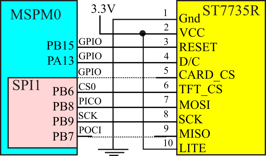
Figure M.5.11. MSPM0G3507 interfaced to the Adafruit ST7735R LCD.
Figure M.5.12. shows the 128 by 160 pixel color display
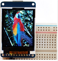
Figure M.5.12. ST7735R display with 160 by 128 16-bit color pixels.
Video M.5.1. Interfacing the ST7735R LCD.
: How does the ST7735R software driver specify color?
Before we output data or commands to the display, we will check a status flag and wait for the previous operation to complete. Busy-wait synchronization is very simple and is appropriate for I/O devices that are fast and predicable. D/C stands for data/command; you will make D/C high to send data and low to send a command. Because the LCD is so fast we will use "busy-wait" synchronization, which means before the software issues an output command to the LCD, it will wait until the display is not busy. In particular, the software will wait for the previous LCD command to complete.
: What does the D/C pin do?
: What does the TFT_CS pin do?
: What does the MOSI pin do?
: What does the SCK pin do?
Video M.5.2. Synchronizing software to hardware.
The following pseudo-code and Figure M.5.13 shows the steps to interact with the LCD using the SPI module. The SPI module uses a first in first out (FIFO) queue built into the hardware. Bit 4 of the SPI1->STAT register is busy. If busy is 1, it means it cannot accept another command at this point. If busy is 0, it means it ready and can accept another command. Bit 1 of the SPI1->STAT register is TNF, which stands for transmitter FIFO not full. If TNF is 0, it means the transmitter FIFO is full and it cannot accept another data output at this point. If TNF is 1, it means the FIFO is not full and can accept another data output. Notice that this interface will wait before and after each command, however multiple data outputs can occur as long as there in room in the FIFO.
writecommand: Involves 6 steps performed to send 8-bit Commands to the
LCD
1. Read SPI1->STAT and check bit 4,
2. If bit 4 is high, loop back to step 1 (wait for BUSY
bit to be low)
3. Clear D/C=PA13 to zero (D/C pin configured for COMMAND)
4. Write the command to SPI1->TXDATA
5. Read SPI1->STAT and check bit 4,
6. If bit 4 is high loop back to step 5 (wait for BUSY bit
to be low)
writedata: Involves 4 steps performed to send 8-bit Data to the LCD:
1. Read SPI1->STAT and check bit 1,
2. If bit 1 is low, loop back to step 1 (wait for TNF bit
to be one)
3. Set D/C=PA13 to one (D/C pin configured for DATA)
4. Write the 8-bit data to SPI1->TXDATA
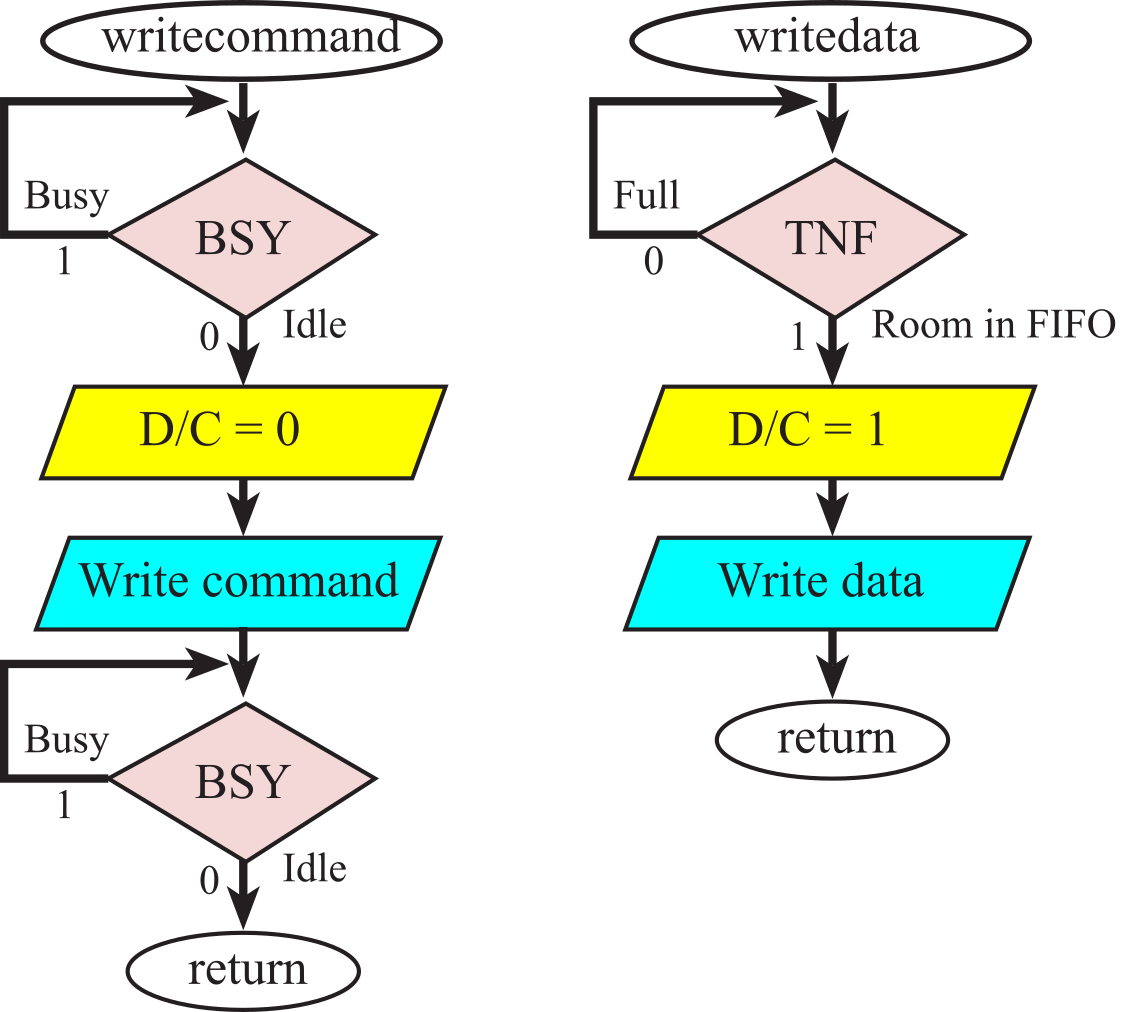
Figure M.5.13. Busy-wait synchronization is used to send commands and data to the display.
: What does busy-wait mean?
There is a rich set of graphics functions available for the ST7735R, allowing you to create amplitude versus time, or bit-mapped graphics. Refer to the ST7735R.h header file for more details.
M.6. MSPM0 I2C Details
MSPM0 microcontrollers have two I2C modules. As shown in Figure M.6.1, microcontroller pins SDA and SCL can be connected directly to an I2C network. Because I2C networks are intended to connect devices on the same PCB, no special hardware interface electronics are required.
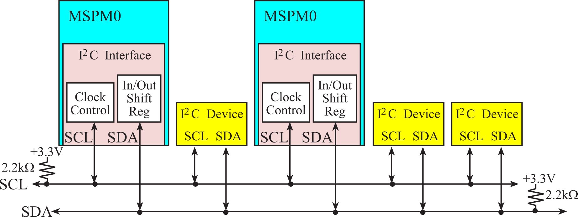
Figure M.6.1. Block diagram of an I2C communication network. Use 1kΩ resistors for fast mode.
Table M.6.1 lists some of the I2C registers on the MSPM0. The MSPM0 can operate in slave mode, but we will focus on master mode. The PF field in the PINCM register can be used to attach I/O pins to the I2C module.
|
|
7 |
6 |
5 |
4 |
3 |
2 |
1 |
0 |
Name |
|
0x400F3214 |
SADDR (bits 10-1) |
DIR |
MSA |
||||||
|
0x400F3218 |
|
BSBSY |
IDLE |
ARBLST |
DATACK |
ADRACK |
ERR |
BUSY |
MSR |
|
0x400F321C |
DATA |
DATA |
DATA |
DATA |
DATA |
DATA |
DATA |
DATA |
MRXDATA |
|
0x400F3220 |
DATA |
DATA |
DATA |
DATA |
DATA |
DATA |
DATA |
DATA |
MTXDATA |
Table M.6.1. The MSPM0 I2C master registers. Each
register is 32 bits wide.
Table M.6.2 lists the available pins for each I2C function.
|
Function |
Pin |
Pin |
Pin |
Pin |
Pin |
Pin |
|
I2C0_SDA |
PA0 (3) |
PA10 (4) |
PA28 (3) |
|
|
|
|
I2C0_SCL |
PA1 (3) |
PA11 (4) |
PA31 (3) |
|
|
|
|
I2C1_SDA |
PA3 (9) |
PA10 (8) |
PA16 (4) |
PA18 (4) |
PA30 (2) |
PB3 (4) |
|
I2C1_SCL |
PA4 (9) |
PA11 (8) |
PA15 (4) |
PA17 (4) |
PA29 (2) |
PB2 (4) |
Table M.6.2. I/O port pins for I2C on the MSPM0. The PINCM PF mode settings are given in parentheses.
Program M.6.1 shows the low-level code needed to interface the SSD1306 to the MSPM0. The display, shown in Figure M.6.2, is connected to PB2 and PB3 and used I2C1. The extra pullup on the SCL line makes it run faster.
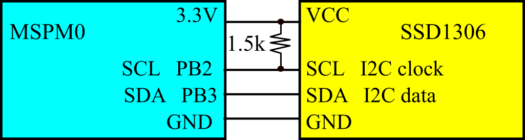
Figure M.6.2. SSD1306 interface uses I2C.
void I2C_Init(void){
// assumes GPIOA and GPIOB are reset and powered previously
I2C1->GPRCM.RSTCTL = 0xB1000003;
I2C1->GPRCM.PWREN = 0x26000001;
// configure PB3 and PB2 as alternate IC2 function
// bit 18 INENA
// bit 25 hiZ
// bit 7 PC peripheral connect
// bits 4-0 I2C
IOMUX->SECCFG.PINCM[PB3INDEX] = 0x02040084; // I2C SDA
IOMUX->SECCFG.PINCM[PB2INDEX] = 0x02040084; // I2C SCL
Clock_Delay(24); // time for gpio to power up
I2C1->CLKSEL = 8; // SYSCLK
// bit 3 SYSCLK
// bit 2 MFCLK
I2C1->CLKDIV = 0; // divide by 1
I2C1->MASTER.MCTR = 0x00;
// period=clockPeriod*(1+MTPR)*10
// bus clock=80MHz, make MTPR=9, frequency = 40MHz/100 = 400kHz
I2C1->MASTER.MTPR = 9; // Set frequency to 400000 Hz
// bits 6-0 TPR (0 to 63), divide by TPR+1
I2C1->MASTER.MCR = 4;
// bit 8 LPBK=0 no loop back
// bit 2 CLKSTRETCH=1 allow stretch
// bit 1 MMST=0 disable multicontroller mode
// bit 0 ACTIVE 0 for disable, 1 for enable
// not using interrupts, FIFO triggers not used
I2C1->MASTER.MFIFOCTL = 0;
I2C1->MASTER.MCR = 5;
}
// receives two bytes from specified slave
uint16_t I2C_Recv2(int8_t slave){
uint8_t data1, data2;
while((I2C1->MASTER.MSR & 0x20) == 0){}; // wait until idle
I2C1->MASTER.MSA = (slave<<1)|0x0001;
// bit 7-1 address
// bit 0 direction=1 receive
I2C1->MASTER.MCTR = 0x00020007;
// bits 27-16 MBLEN =2 (length)
// bit 3 ACK
// bit 2 STOP=1
// bit 1 START=1
// bit 0 BURSTRUN=1
while((I2C1->MASTER.MFIFOSR & 0x000F) == 0){}; //wait for received data
data1 = I2C1->MASTER.MRXDATA;
while((I2C1->MASTER.MFIFOSR & 0x000F) == 0){}; //wait for received data
data2 = I2C1->MASTER.MRXDATA;
return (data1<<8)+data2;
}
int static IC2FillTxFifo(uint8_t *buffer, uint16_t count){
for(int i=0; i<count; i++){
if((I2C1->MASTER.MFIFOSR & 0x0F00) == 0) return 0; // fail TxFifo can't take data
I2C1->MASTER.MTXDATA = buffer[i];
}
return 1;
}
uint32_t I2C_error;
// count must be less than 8, because it fills the FIFO before starting
int I2C_Send(uint8_t slave, uint8_t *pData, uint32_t count){
if(count>8){
I2C_error = count; // help debugging
return 0; // error
}
if(IC2FillTxFifo(pData,count) == 0) return 0;
while((I2C1->MASTER.MSR & 0x20) == 0){}; // wait until idle
I2C1->MASTER.MSA = (slave<<1);
// bit 7-1 address
// bit 0 direction=0 transmit
I2C1->MASTER.MCTR = 0x00000007|(count<<16);
// bits 27-16 MBLEN =count (length)
// bit 3 ACK
// bit 2 STOP=1
// bit 1 START=1
// bit 0 BURSTRUN=1
while((I2C1->MASTER.MSR & 0x01) == 0x01){}; // wait until not busy
// check for error
if(I2C1->MASTER.MSR & 0x12){ // lost arbitration or no ack
I2C_error = I2C1->MASTER.MSR; // help debugging
return 0; // error
}
while((I2C1->MASTER.MSR & 0x20) == 0){}; // wait until idle
return 1;
}
Program M.6.1. MSPM0 I2C software in single master mode.
Timing is complicated and potentially confusing. Fortunately, it is handled by hardware you are already given. There are two complicated things for which you are responsible. The first issue is understanding what codes to send to the I2C slave. The second complicated issue is what bits to write to MASTER.MCTR.
Figure M.6.6 shows a logic analyzer measurement taken with Program M.6.3 communicating with a Texas Instruments TMP102 thermometer. The main program calls I2C_Recv2(0x48); The first transmission sends the 0x91 (slave address, read) command. It then receives two transmissions, which is the temperature encoded with 0.0625°C resolution.

Figure M.6.6. Logic analyzer transmission of I2C_Recv2, with one output and two inputs.
I2C can be very difficult to configure. We suggest you observe the SCL and SDL on an oscilloscope. First check the clock rate and second verify the output high and output low voltages are within specification. Look up VIH and VIL of both the microcontroller and the remote sensor. The high voltage measured by the scope should be higher than VIH of both devices. The low voltage measured by the scope should be lower than VIL of both devices.
M.7. Edge-triggered Interrupts
Synchronizing software to hardware events requires the software to recognize when the hardware changes states from busy to done. Many times the busy to done state transition is signified by a rising (or falling) edge on a status signal in the hardware. For these situations, we connect this status signal to an input of the microcontroller, and we use edge-triggered interfacing to configure the interface to set a flag on the rising (or falling) edge of the input. Using edge-triggered interfacing allows the software to respond quickly to changes in the external world. If we are using busy-wait synchronization, the software waits for the flag. If we are using interrupt synchronization, we configure the flag to request an interrupt when set. Each of the digital I/O pins on the MSPM0 family can be configured for edge triggering.
Table M.7.1 shows the polarity configuration bits for edge-triggered interrupts. There are four polarity registers to specify the active edge for each of the 60 pins on the MSPM0. Let edgxx be the 2-bit field for pin xx.
edgxx=00 none
edgxx=01 rising edge
edgxx=10 falling edge
edgxx=11 both edges
|
|
31-30 |
29-28 |
27-26 |
25-24 |
23-22 |
... |
3-2 |
1-0 |
|
GPIOA->POLARITY15_0 |
edg15 |
edg14 |
edg13 |
edg12 |
edg11 |
... |
edg1 |
edg0 |
|
GPIOA->POLARITY31_16 |
edg31 |
edg30 |
edg29 |
edg28 |
edg27 |
... |
edg17 |
edg16 |
|
GPIOB->POLARITY15_0 |
edg15 |
edg14 |
edg13 |
edg12 |
edg11 |
... |
edg1 |
edg0 |
|
GPIOB->POLARITY31_16 |
-- |
-- |
-- |
-- |
edg27 |
... |
edg17 |
edg16 |
Table M.7.1. Polarity registers for edge-triggered interrupts.
Table M.7.2 shows three more registers needed to configure edge-triggered interrupts. Each of the 60 pins has an arm bit in one of the two IMASK registers. If the arm bit is 1 then that pin is armed for interrupts. The two RIS registers contain the 60 trigger flags. A bit set in the RIS register means that pin had an active edge. The ICLR register is used to acknowledge the interrupt. Writing ones to a ICLR register will clear the cooresponding bits in the RIS register. The ICLR registers are write only. We should not read them. Writing zeros to the ICLR registers has no affect.
|
|
31 |
30 |
29 |
28 |
27 |
... |
1 |
0 |
|
GPIOA->CPU_INT.IMASK |
arm31 |
arm30 |
arm29 |
arm28 |
arm27 |
... |
arm1 |
arm0 |
|
GPIOA->CPU_INT.ICLR |
clr31 |
clr30 |
clr29 |
clr28 |
clr27 |
... |
clr1 |
clr0 |
|
GPIOA->CPU_INT.RIS |
ris15 |
ris30 |
ris29 |
ris28 |
ris27 |
... |
ris1 |
ris0 |
|
GPIOB->CPU_INT.IMASK |
-- |
-- |
-- |
-- |
arm27 |
... |
arm1 |
arm0 |
|
GPIOB->CPU_INT.ICLR |
-- |
-- |
-- |
-- |
clr27 |
... |
clr1 |
clr0 |
|
GPIOB->CPU_INT.RIS |
-- |
-- |
-- |
-- |
ris27 |
... |
ris1 |
ris0 |
Table M.7.2. Registers for edge-triggered interrupts.
Program M.7.1 configures PB21 to interrupt on the falling edge. See Figure M.7.1. shows the negative logic switch interface to PB21. Because it is negative logic, the interrupt will occur when the operator touches the switch.
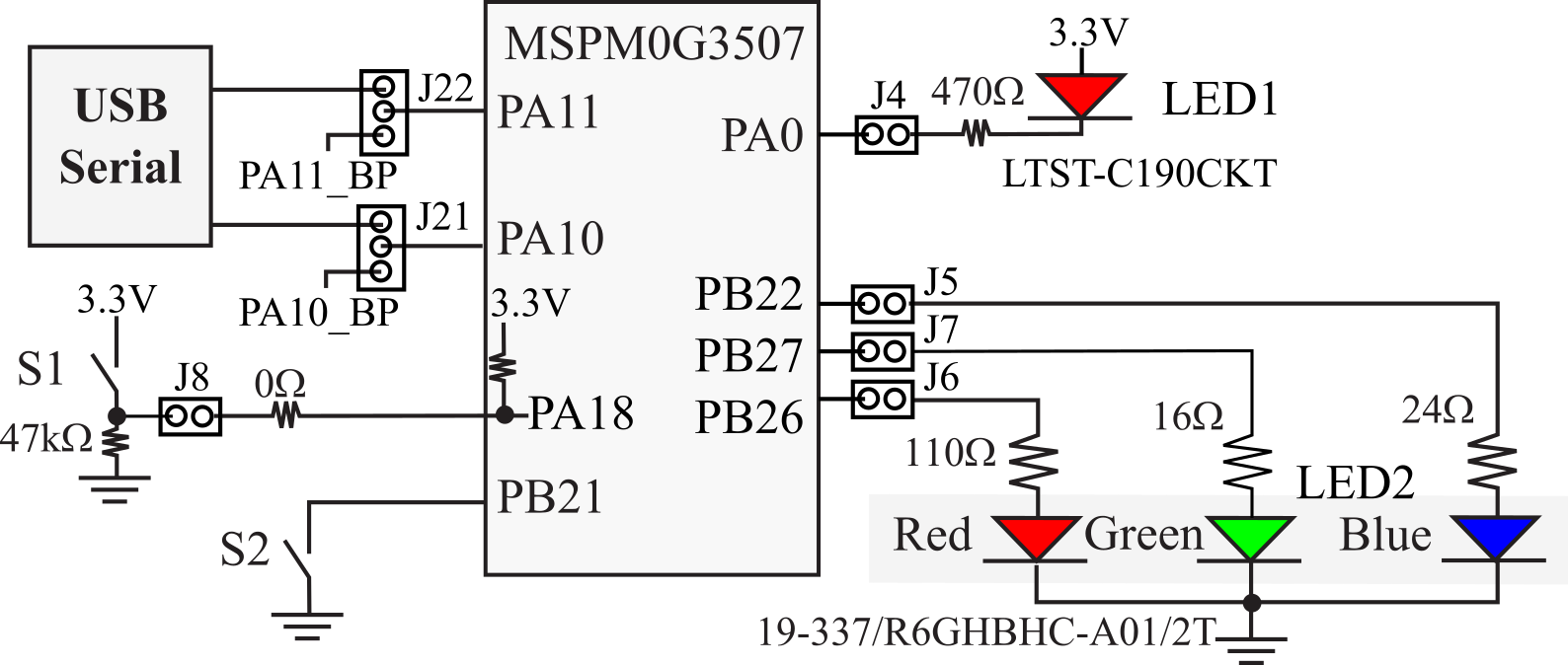
Figure M.7.1. Switch and LED interfaces on the MSPM0G3507 LaunchPad Evaluation Board (same as Figure 1.6.13).
// Arm interrupts on fall of PB21
// interrupts will be enabled in main after all initialization
void EdgeTriggered_Init(void){
GPIOB->POLARITY31_16 = 0x00000800; // falling of PB21
GPIOB->CPU_INT.ICLR = 0x00200000; // clear bit 21
GPIOB->CPU_INT.IMASK = 0x00200000; // arm PB21
NVIC->IP[0] = (NVIC->IP[0]&(~0x0000FF00))|2<<14; // set priority (bits 15,14) IRQ 1
NVIC->ISER[0] = 1 << 1; // Group1 interrupt
}
uint32_t Count; // number of times switch is pressed
int main(void){
__disable_irq();
LaunchPad_Init(); // PB21 is input with internal pull up resistor
EdgeTriggered_Init();
Count = 0;
__enable_irq();
while(1){
GPIOB->DOUTTGL31_0 = GREEN; // toggle PB27
}
}
// called on the falling edge of PB21
void GROUP1_IRQHandler(void){
Count++; // number of touches
GPIOB->DOUTTGL31_0 = RED; // toggle PB26
GPIOB->CPU_INT.ICLR = 0x00200000; // clear bit 21
}
Program M.7.1. Using interrupts to count switch touches.
In this second example, we connect positive logic switches to PA8, PA22, PB18, and PB24. The goal is to count the number of times each switch is touched. Program M.7.2 configures each of these four pins to interrupt on the rising edge. Because the switches are positive logic, a rising edge trigger will occur when the operator touches the switch. This is an example of a polled interrupt, because the ISR must poll each of the possible sources to determine which source triggered the interrupt.
Video M.7.1. Edge-Triggered Interrupts.
void EdgeTriggered_Init(void){
LaunchPad_Init(); // PB21 is input with internal pull up resistor
IOMUX->SECCFG.PINCM[PB18INDEX] = 0x00040081; // input
IOMUX->SECCFG.PINCM[PB24INDEX] = 0x00040081; // input
IOMUX->SECCFG.PINCM[PA22INDEX] = 0x00040081; // input
IOMUX->SECCFG.PINCM[PA8INDEX] = 0x00040081; // input
GPIOA->POLARITY15_0 = (1<<(8<<1)); // PA8 rising
GPIOA->POLARITY31_16 = (1<<((22-16)<<1)); // PB22 rising
GPIOB->POLARITY31_16 = (1<<((18-16)<<1))+ // PB18 rising
(1<<((24-16)<<1)); // PB24 falling
GPIOA->CPU_INT.ICLR = (1<<8)|(1<<22); // clear bit 8,22
GPIOB->CPU_INT.ICLR = (1<<24)|(1<<18); // clear bit 18,24
GPIOA->CPU_INT.IMASK = (1<<8)|(1<<22); // arm PA8 and PA22
GPIOB->CPU_INT.IMASK = (1<<24)|(1<<18); // arm PB18 and PB24
NVIC->IP[0] = (NVIC->IP[0]&(~0x0000FF00))|2<<14; // set priority (bits 15,14) IRQ 1
NVIC->ISER[0] = 1 << 1; // Group1 interrupt
}
uint32_t CountPA8,CountPB18,CountPA22,CountPB24;
int main(void){
__disable_irq();
Clock_Init80MHz(0);
EdgeTriggered_Init();
CountPA8=CountPB18=CountPA22=CountPB24=0;
__enable_irq();
while(1){
// other stuff
}
}
// rising edge on PB18, PB24, PA22, PA8
void GROUP1_IRQHandler(void){
if(GPIOA->CPU_INT.RIS&(1<<8)){ // PA8
GPIOA->CPU_INT.ICLR = 1<<8;
CountPA8++; // number of touches
}
if(GPIOA->CPU_INT.RIS&(1<<22)){ // PA22
GPIOA->CPU_INT.ICLR = 1<<22;
CountPA22++;
}
if(GPIOB->CPU_INT.RIS&(1<<18)){ // PB18
GPIOB->CPU_INT.ICLR = 1<<18;
CountPB18++; // number of touches
}
if(GPIOB->CPU_INT.RIS&(1<<24)){ // PB24
GPIOB->CPU_INT.ICLR = 1<<24;
CountPB24++;
}
}
Program M.7.2. Using interrupts to count touches on four positive logic switches.
M.8. Pulse Width Modulation using the Timer Module
Generating output waves is an essential task for real-time systems, so microcontrollers have multiple methods to create digital output waves.
Pulse width modulation is an effective and thus popular mechanism for the embedded microcontrollers to control external devices. On the MSPM0 each Timer module can create one to four PWM outputs with a common period but differing the duty cycles. In this example, Timer G6 is set to down mode. PWM outputs can also be created with up mode, but in this section we will describe down mode. In the examples below, we make High plus Low be a constant. By adjusting the ratio of High and Low the software can control the duty cycle.
In this example, we begin by reseting and activating Timer G6.
Timer G6 is in power domain PD1, so it operates at 80 MHz.
We set the alternate function mode for PB6 to attach it to function Timer G6 CCP0.
Referring to the PINCM register, we see PB6 Timer G6 CCP0 is mode 7.
PB6 is an output so we enable its output driver. We set the clock source to the 80 MHz bus clock.
We set TIMG6->CLKDIV to 0 to select a divide by 1.
The user specifies prescale and load to establish the period of the PWM output.
PWM Freq = (80MHz / (prescale * period))
PWM Period = (12.5ns * (prescale * period))
This implementation occurs in hardware and does not require interrupts.
Therefore, it can generate waves close to 0 or 100% duty cycle.
Figure M.8.1 shows a system using one PWM output to control the steering servo motor.
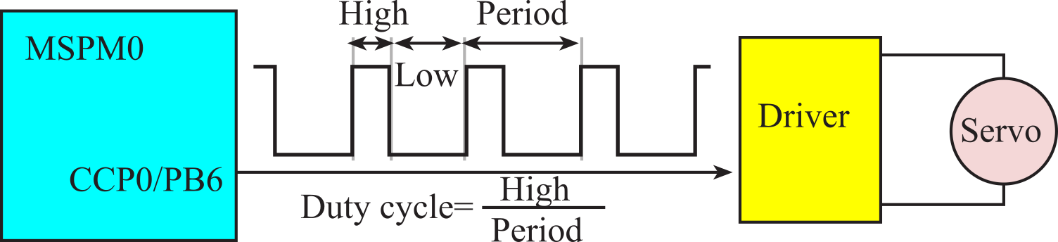
Figure M.8.1. The PWM output can set the angle on the robot steering servo.
Program M.8.1 configures Timer G0 for one PWM output. The user calls PWMG6_Init once to turn it on, and then calls PWMG6_SetDuty to adjust the duty cycle. To control the servo, the system outputs 20-ms square wave, with a high pulse from 0.5 to 2.5ms, as shown in Figure M.8.2.
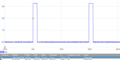
Figure M.8.2. The PWM output can set the angle on the robot steering servo.
Program M.8.1 shows the low-level code to create a PWM output.
void PWMG6_Init(uint32_t prescale, uint32_t period, uint32_t duty){
TIMG6->GPRCM.RSTCTL = (uint32_t)0xB1000003;
TIMG6->GPRCM.PWREN = (uint32_t)0x26000001;
Clock_Delay(24); // time for TimerG6 to power up
IOMUX->SECCFG.PINCM[PB6INDEX] = 0x00000087; // TIMG6 output CCP0
GPIOB->DOE31_0 |= (1<<6);
TIMG6->CLKSEL = 8; // 8=BUSCLK, 4= MFCLK, 2= LFCLK clock
TIMG6->CLKDIV = 0x00; // divide by 1
TIMG6->COMMONREGS.CPS = prescale-1; // divide by prescale,
// 32768Hz/256 = 256Hz, 7.8125
TIMG6->COUNTERREGS.LOAD = period-1; // reload register sets period
PWMG6_Period = period;
TIMG6->COUNTERREGS.CTRCTL = 0x02;
// bits 5-4 CM =0, down
// bits 3-1 REPEAT =001, continue
// bit 0 EN enable (0 for disable, 1 for enable)
TIMG6->COUNTERREGS.CCCTL_01[0] = 0; // no capture
// COC compare mode
TIMG6->GEN_EVENT0.IMASK = 0x00; // no interrupts
TIMG6->COMMONREGS.CCPD = 0x01; // output CCP0
TIMG6->COMMONREGS.CCLKCTL = 1;
TIMG6->COUNTERREGS.CC_01[0] = PWMG6_Period-duty;
TIMG6->COUNTERREGS.OCTL_01[0] = 0x0000; // connected to PWM
TIMG6->COUNTERREGS.CCACT_01[0] = 0x0088;
// bits 10-9 CUACT 0 for no action on up compare
// bits 7-6 CDACT 10 for make low on compare event down
// bits 4-3 LACT 01 for make high on load event
// bits 1-0 ZACT 00 for no action on zero event
TIMG6->COUNTERREGS.CTRCTL |= 0x01;
}
void PWMG6_SetDuty(uint32_t duty){
TIMG6->COUNTERREGS.CC_01[0] = PWMG6_Period-duty;
}
Program M.8.1. Software to generate a PWM output using Timer G6.
: What event in the timer makes PB6 go high?
: What event in the timer makes PB6 go low?
: What parameters do we invoke PWMG6_Init to get a 20ms period, 2ms high?
: Assume an 80 MHz bus clock and we invoke PWMG6_Init(80,10000,2500). What is the period of the wave? What is the duty cycle? What is the precision (number of different duty cycles that can be created by calling PWMG6_SetDuty?
M.9. Input Capture Details on the MSPM0
M.9.1. Input Capture Concepts
The goal of this section to measure the period or pulse width of digital-level signals. We connect a digital input to a timer pin and use input capture to perform the measurement. The basic principles of input capture are presented in Section 8.2. In this section, we present details for the MSPM0 microcontroller.
The MSPM0G3507 microcontroller has 7 timers, which can be used to create periodic interrupts. Timer G12 is a 32-bit hardware timer with no prescale; the other six are 16-bit timers with an 8-bit prescale. Each timer has a counter register, e.g., TIMG0->COUNTERREGS.CTR, which is decremented automatically in hardware. The 7 timers are listed in Table M.9.1. In input capture mode, the CTR register continuously counts down. Timers G0 and G8 are clocked at one half the bus frequency. Timers A0, A1, G6, G7, and G12 are clocked at the bus frequency. All timers except G12 have a clock prescale=CPS register containing an 8-bit prescale.
|
Load |
Prescale |
ULPCLK |
Power
Domain |
|
|
TimerA0 |
16 bit |
8 bit |
80MHz |
PD1 |
|
TimerA1 |
16 bit |
8 bit |
80MHz |
PD1 |
|
TimerG0 |
16 bit |
8 bit |
40MHz |
PD0 |
|
TimerG12 |
32 bit |
none |
80MHz |
PD1 |
|
TimerG6 |
16 bit |
8 bit |
80MHz |
PD1 |
|
TimerG7 |
16 bit |
8 bit |
80MHz |
PD1 |
|
TimerG8 |
16 bit, |
8 bit |
40MHz |
PD0 |
Table M.9.1. Details on the 7 hardware timers.
If the bus clock period is Δt, then the timer counting period is
Δt*(CPS+1)*2 for G0 and G8
Δt*(CPS+1) for A0, A1, G6, G7, and G12
Resolution is the smallest difference between two inputs that can be reliably measured. The timer counting period will set the resolution of the input capture measurement. If we make the CPS=39 with a bus clock at 80 MHz, then Timer G0 counts down at 1 MHz (every 1us). For input capture mode, we set the LOAD register to its maximum value, which is 0xFFFFFFFF on G12 and 0xFFFF on the other six timers. The timer counts down from LOAD to 0. On the next count, the CTR register is reloaded with the value in LOAD. In 16-bit input capture mode, the CTR register continuously counts
0xFFFF, 0xFFFE, 0xFFFD,...2, 1, 0, 0xFFFF, 0xFFFE, 0xFFFD,...
Input edge time mode (or input capture mode) is used to make time measurements on input signals. The active edge of the input signal will capture the counter into the latch, see Figure M.9.1
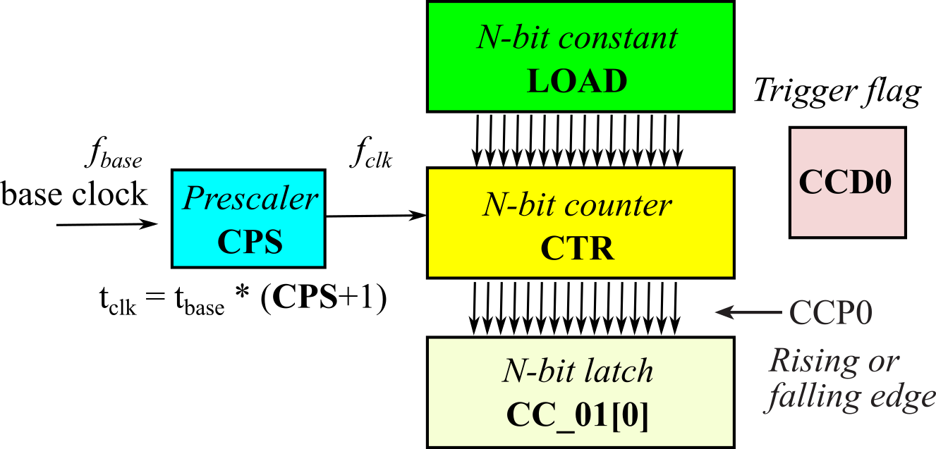
Figure M.9.1. Rising or falling edge of CCP0 causes the counter CTR to be latched into CC_01[0], setting the CCD0 flag.
Each input capture module has
An external input pin, e.g., TIMG0_C0
A trigger flag bit, in the RIS register , e.g., CCD0 is set on a capture of TIMG0_C0 pin
Three edge control bits in the CCCTL_01 register, e.g., set CCOND to 001 to select rising edge
An arm bit in the CPU_INT.IMASK register, e.g., set bit 4, CCD0, to arm
A 16-bit or 32-bit counter, e.g., TIMG0->COUNTERREGS.CTR
A 16-bit or 32-bit input capture latch, e.g., TIMG0->COUNTERREGS.CC_01[0] contains the counter value at last capture
Table M.9.2 shows virtually every pin on the MSPM0G3507 can be used for input capture. The input capture pins are labeled TIMA0_C0, TIMA_C1, ... For example TIMG8_C1 is the input capture pin for Timer G8, submodule C1.
|
PINCM |
Pin |
Mode2 |
Mode3 |
Mode4 |
Mode5 |
Mode6 |
Mode7 |
Mode8 |
|
1 |
PA0 |
UART0_TX |
I2C0_SDA |
TIMA0_C0 |
TIMA_FAL1 |
TIMG8_C1 |
FCC_IN |
|
|
2 |
PA1 |
UART0_RX |
I2C0_SCL |
TIMA0_C1 |
TIMA_FAL2 |
TIMG8_IDX |
TIMG8_C0 |
|
|
7 |
PA2 |
TIMG8_C1 |
SPI0_CS0 |
TIMG7_C1 |
SPI1_CS0 |
|||
|
8 |
PA3 |
TIMG8_C0 |
SPI0_CS1 |
UART2_CTS |
TIMA0_C2 |
COMP1_OUT |
TIMG7_C0 |
TIMA0_C1 |
|
9 |
PA4 |
TIMG8_C1 |
SPI0_POCI |
UART2_RTS |
TIMA0_C3 |
LFCLK_IN |
TIMG7_C1 |
TIMA0_C1N |
|
10 |
PA5 |
TIMG8_C0 |
SPI0_PICO |
TIMA_FAL1 |
TIMG0_C0 |
TIMG6_C0 |
FCC_IN |
|
|
11 |
PA6 |
TIMG8_C1 |
SPI0_SCK |
TIMA_FAL0 |
TIMG0_C1 |
HFCLK_IN |
TIMG6_C1 |
TIMA0_C2N |
|
14 |
PA7 |
COMP0_OUT |
CLK_OUT |
TIMG8_C0 |
TIMA0_C2 |
TIMG8_IDX |
TIMG7_C1 |
TIMA0_C1 |
|
19 |
PA8 |
UART1_TX |
SPI0_CS0 |
UART0_RTS |
TIMA0_C0 |
TIMA1_C0N |
||
|
20 |
PA9 |
UART1_RX |
SPI0_PICO |
UART0_CTS |
TIMA0_C1 |
RTC_OUT |
TIMA0_C0N |
TIMA1_C1N |
|
21 |
PA10 |
UART0_TX |
SPI0_POCI |
I2C0_SDA |
TIMA1_C0 |
TIMG12_C0 |
TIMA0_C2 |
I2C1_SDA |
|
22 |
PA11 |
UART0_RX |
SPI0_SCK |
I2C0_SCL |
TIMA1_C1 |
COMP0_OUT |
TIMA0_C2N |
I2C1_SCL |
|
34 |
PA12 |
UART3_CTS |
SPI0_SCK |
TIMG0_C0 |
CAN_TX |
TIMA0_C3 |
FCC_IN |
|
|
35 |
PA13 |
UART3_RTS |
SPI0_POCI |
UART3_RX |
TIMG0_C1 |
CAN_RX |
TIMA0_C3N |
|
|
36 |
PA14 |
UART0_CTS |
SPI0_PICO |
UART3_TX |
TIMG12_C0 |
CLK_OUT |
||
|
37 |
PA15 |
UART0_RTS |
SPI1_CS2 |
I2C1_SCL |
TIMA1_C0 |
TIMG8_IDX |
TIMA1_C0N |
TIMA0_C2 |
|
38 |
PA16 |
COMP2_OUT |
SPI1_POCI |
I2C1_SDA |
TIMA1_C1 |
TIMA1_C1N |
TIMA0_C2N |
FCC_IN |
|
39 |
PA17 |
UART1_TX |
SPI1_SCK |
I2C1_SCL |
TIMA0_C3 |
TIMG7_C0 |
TIMA1_C0 |
|
|
40 |
PA18 |
UART1_RX |
SPI1_PICO |
I2C1_SDA |
TIMA0_C3N |
TIMG7_C1 |
TIMA1_C1 |
|
|
46 |
PA21 |
UART2_TX |
TIMG8_C0 |
UART1_CTS |
TIMA0_C0 |
TIMG6_C0 |
||
|
47 |
PA22 |
UART2_RX |
TIMG8_C1 |
UART1_RTS |
TIMA0_C1 |
CLK_OUT |
TIMA0_C0N |
TIMG6_C1 |
|
53 |
PA23 |
UART2_TX |
SPI0_CS3 |
TIMA0_C3 |
TIMG0_C0 |
UART3_CTS |
TIMG7_C0 |
TIMG8_C0 |
|
54 |
PA24 |
UART2_RX |
SPI0_CS2 |
TIMA0_C3N |
TIMG0_C1 |
UART3_RTS |
TIMG7_C1 |
TIMA1_C1 |
|
55 |
PA25 |
UART3_RX |
SPI1_CS3 |
TIMG12_C1 |
TIMA0_C3 |
TIMA0_C1N |
||
|
59 |
PA26 |
UART3_TX |
SPI1_CS0 |
TIMG8_C0 |
TIMA_FAL0 |
CAN_TX |
TIMG7_C0 |
|
|
60 |
PA27 |
RTC_OUT |
SPI1_CS1 |
TIMG8_C1 |
TIMA_FAL2 |
CAN_RX |
TIMG7_C1 |
|
|
3 |
PA28 |
UART0_TX |
I2C0_SDA |
TIMA0_C3 |
TIMA_FAL0 |
TIMG7_C0 |
TIMA1_C0 |
|
|
4 |
PA29 |
I2C1_SCL |
UART2_RTS |
TIMG8_C0 |
TIMG6_C0 |
|||
|
5 |
PA30 |
I2C1_SDA |
UART2_CTS |
TIMG8_C1 |
TIMG6_C1 |
|||
|
6 |
PA31 |
UART0_RX |
I2C0_SCL |
TIMA0_C3N |
TIMG12_C1 |
CLK_OUT |
TIMG7_C1 |
TIMA1_C1 |
|
12 |
PB0 |
UART0_TX |
SPI1_CS2 |
TIMA1_C0 |
TIMA0_C2 |
|||
|
13 |
PB1 |
UART0_RX |
SPI1_CS3 |
TIMA1_C1 |
TIMA0_C2N |
|||
|
15 |
PB2 |
UART3_TX |
UART2_CTS |
I2C1_SCL |
TIMA0_C3 |
UART1_CTS |
TIMG6_C0 |
TIMA1_C0 |
|
16 |
PB3 |
UART3_RX |
UART2_RTS |
I2C1_SDA |
TIMA0_C3N |
UART1_RTS |
TIMG6_C1 |
TIMA1_C1 |
|
17 |
PB4 |
UART1_TX |
UART3_CTS |
TIMA1_C0 |
TIMA0_C2 |
TIMA1_C0N |
||
|
18 |
PB5 |
UART1_RX |
UART3_RTS |
TIMA1_C1 |
TIMA0_C2N |
TIMA1_C1N |
||
|
23 |
PB6 |
UART1_TX |
SPI1_CS0 |
SPI0_CS1 |
TIMG8_C0 |
UART2_CTS |
TIMG6_C0 |
TIMA1_C0N |
|
24 |
PB7 |
UART1_RX |
SPI1_POCI |
SPI0_CS2 |
TIMG8_C1 |
UART2_RTS |
TIMG6_C1 |
TIMA1_C1N |
|
25 |
PB8 |
UART1_CTS |
SPI1_PICO |
TIMA0_C0 |
COMP1_OUT |
|||
|
26 |
PB9 |
UART1_RTS |
SPI1_SCK |
TIMA0_C1 |
TIMA0_C0N |
|||
|
27 |
PB10 |
TIMG0_C0 |
TIMG8_C0 |
COMP1_OUT |
TIMG6_C0 |
|||
|
28 |
PB11 |
TIMG0_C1 |
TIMG8_C1 |
CLK_OUT |
TIMG6_C1 |
|||
|
29 |
PB12 |
UART3_TX |
TIMA0_C2 |
TIMA_FAL1 |
TIMA0_C1 |
|||
|
30 |
PB13 |
UART3_RX |
TIMA0_C3 |
TIMG12_C0 |
TIMA0_C1N |
|||
|
31 |
PB14 |
SPI1_CS3 |
SPI1_POCI |
SPI0_CS3 |
TIMG12_C1 |
TIMG8_IDX |
TIMA0_C0 |
|
|
32 |
PB15 |
UART2_TX |
SPI1_PICO |
UART3_CTS |
TIMG8_C0 |
TIMG7_C0 |
||
|
33 |
PB16 |
UART2_RX |
SPI1_SCK |
UART3_RTS |
TIMG8_C1 |
TIMG7_C1 |
||
|
43 |
PB17 |
UART2_TX |
SPI0_PICO |
SPI1_CS1 |
TIMA1_C0 |
TIMA0_C2 |
||
|
44 |
PB18 |
UART2_RX |
SPI0_SCK |
SPI1_CS2 |
TIMA1_C1 |
TIMA0_C2N |
||
|
45 |
PB19 |
COMP2_OUT |
SPI0_POCI |
TIMG8_C1 |
UART0_CTS |
TIMG7_C1 |
||
|
48 |
PB20 |
SPI0_CS2 |
SPI1_CS0 |
TIMA0_C2 |
TIMG12_C0 |
TIMA_FAL1 |
TIMA0_C1 |
TIMA1_C1N |
|
49 |
PB21 |
SPI1_POCI |
TIMG8_C0 |
|||||
|
50 |
PB22 |
SPI1_PICO |
TIMG8_C1 |
|||||
|
51 |
PB23 |
SPI1_SCK |
COMP0_OUT |
TIMA_FAL0 |
||||
|
52 |
PB24 |
SPI0_CS3 |
SPI0_CS1 |
TIMA0_C3 |
TIMG12_C1 |
TIMA0_C1N |
TIMA1_C0N |
|
|
56 |
PB25 |
UART0_CTS |
SPI0_CS0 |
TIMA_FAL2 |
||||
|
57 |
PB26 |
UART0_RTS |
SPI0_CS1 |
TIMA0_C3 |
TIMG6_C0 |
TIMA1_C0 |
||
|
58 |
PB27 |
COMP2_OUT |
SPI1_CS1 |
TIMA0_C3N |
TIMG6_C1 |
TIMA1_C1 |
Table M.9.2. Table M.1.5 PINCM is redrawn highlighting pins available for input capture. PF field values for the PINCM register.
In this book we use the term arm to describe the bit that allows/denies a specific flag from requesting an interrupt. The Texas Instruments manuals refer to this bit as a mask. I.e., the device is armed when the mask bit is 1. Typically, there is a separate arm bit for every flag that can request an interrupt. An external digital signal is connected to the input capture pin. During initialization we specify whether the rising or falling edge of the external signal will trigger an input capture event. The 16-bit counter decrements at the rate of the bus clock, when it hits 0, it automatically rolls over to 0xFFFF and continues to count down (Figure M.9.1). Let m be the timer: A0, A1, G0, G6, G7, G8 or G12. Let n be the timer pin number: 0, 1, 2, or 3. For example, TIMG8_C1 is timer G8 pin 1. Three actions result from an input capture event:
1) the current timer value is copied into the input capture register (COUNTERREGS.CC_01[n]),
2)the input capture flag is set (CCDn) and 3) an interrupt is requested if armed
(IM).
The input capture mechanism has many uses. For input
capture, an external digital signal is connected to an input (TIMm_Cn)
of the microcontroller. Three of common applications are: 1. An ISR is executed on the active edge of the
external signal 2. Perform two rising edge input captures and
subtract the two to get period 3. Perform a rising edge and then a falling edge
capture and subtract the two measurements to get pulse width Observation: The timer is very accurate because of the stability of
the crystal clock. Observation: When
measuring period or pulse-width, the measurement resolution will equal the bus
clock period times the prescale value. The basic idea of period
measurement is to generate two input captures on the same edge (both rise or
both fall), record the times of each edge, and calculate the period as the
difference between those two times. Before one implements a system that measures
period, it is appropriate to consider the issues of resolution, precision and range. The resolution of a period measurement
M.9.2. Period Measurement
The precision of the period measurement is defined as the number of separate and distinguishable measurements. If the 16-bit counter is used, there are about 65536 different periods that can be measured. We can specify the precision in alternatives, e.g., 216, or in bits, e.g., 16 bits.
The last issue to consider is the range of the period measurement, which is defined as the minimum and maximum values that can reliably be measured. We are concerned what happens if the period is too small or too large. For this example, the minimum and maximum periods depend on the time to run the ISR. For example, let's allocate the ISR execution time to be 20µs. Therefore the minimum period we can measure will be 20µs and the maximum period will be 65516µs. A good measurement system should be able to detect overflows and underflows. In addition, we would not like the system to crash, or hang-up if the input period is out of range. Similarly, it is desirable if the system can detect when there is no period. For edge detection, the input must be high for at least two system clock periods and low for at least two system clock periods. I, ECE445L Lab 8, we will add a separate periodic interrupt to detect period too large or no period at all (stopped motor).
We begin initialization by enabling the clock for the timer and for the digital port we will be using. We enable the digital pin and select its alternative function. Table M.9.3 lists the edge capture modes CCOND in the CCCTL_01 register.) Program M.9.1 measures the period on PA12 (TIMG0_C0). Please refer to the timer chapter in MSPM0 technical reference manual for more details.
|
CCOND |
Active edge |
|
000 |
None |
|
001 |
Capture on rising |
|
010 |
Capture on falling |
|
011 |
Capture on both rising and falling |
Table M.9.2. Three control bits define the active edge used for input capture.
uint32_t Time,Last,Period;
void InputCapture_Init(uint32_t prescale, uint32_t priority){
TIMG0->GPRCM.RSTCTL = 0xB1000003;
TIMG0->GPRCM.PWREN = 0x26000001;
Clock_Delay(24); // time for TimerG0 to power up
IOMUX->SECCFG.PINCM[PA12INDEX] = 0x00040084; // TIMG0 CCP0
TIMG0->CLKSEL = 8; // 8=BUSCLK, 4= MFCLK, 2= LFCLK clock
TIMG0->CLKDIV = 0x00; // divide by 1
TIMG0->COMMONREGS.CPS = prescale-1; // divide by prescale,
TIMG0->COUNTERREGS.LOAD = 0xFFFF; // set reload register
// interrupts at rising edge of PA12
TIMG0->COUNTERREGS.CTRCTL = 0x02;
// bits 5-4 CM =0, down
// bits 3-1 REPEAT =001, continue
// bit 0 EN enable (0 for disable, 1 for enable)
TIMG0->COUNTERREGS.CCCTL_01[0] = 0x00020001;
// CCCTL_01
// bit 17 1 capture
// bits 14-12 ZCOND zero condition
// bits 10-8 LCOND load condition
// bits 6-4 ACOND advance condition
// bits 2-0 CCOND capture condition, 1 is rising edge of CCP
TIMG0->CPU_INT.IMASK |= 0x10; // CCD0 mask
TIMG0->COMMONREGS.CCLKCTL = 1;
TIMG0->COUNTERREGS.IFCTL_01[0] = 0x0002;
// bit 12 FE =0 bypass
// bit 11 CPV=0 voting
// bit 9-8 FP=00 filter period 3
// bit 7 INV=0 noninverted
// bits 3-0 =0010 input is CCP0
NVIC->ISER[0] = 1 << 16; // TIMG0 interrupt
NVIC->IP[4] = (NVIC->IP[4]&(~0x000000FF))|(priority<<6);
// set priority (bits 7,6) IRQ 16
TIMG0->COUNTERREGS.CTRCTL |= 0x01;
}
void TIMG0_IRQHandler(void){uint32_t iidx;
iidx = TIMG0->CPU_INT.IIDX;// this will acknowledge
if((iidx) == 5){ // 5 means capture CCD0
Time = TIMG0->COUNTERREGS.CC_01[0]; // time now
Period = (Last-Time)&0xFFFF; // elapsed time since last
Last = Time;
}
}
Program M.9.1. Period Measurement.
M.9.3. Pulse width measurement
In this section
we will design a system to measure pulse width using
interrupts, with a precision of 16 bits and a resolution of 1 µs.
In this example, the digital-level input
signal is connected to two input capture pins, PB8/CCP0/TIMA0_C0
and PB12/CCP1/TIMA0_C1 (Figure M.9.3). The bus clock is selected to be 80 MHz, Timer A0 module
clock runs at 80 MHz, and the prescale is 80, so the
measurement resolution will be 1 µs. The rising edge time will be
measured by CCP1 without the need of an
interrupt and the falling edge interrupts will be handled by CCP0. The pulse width is calculated as the
difference in
TIMA0->COUNTERREGS.CC_01[1]-TIMA0->COUNTERREGS.CC_01[0]
In this example the TIMA0_IRQHandler
interrupt handler simply sets the global variable, PW, at the time of the falling edge. Because no
software is required to process the CCP1
measurement, there is no software limit to the minimum pulse width. There is
the hardware limit requiring at least two bus clock periods while high and two
bus clock periods while low. On the other hand, software processing is required
to handle the TIMA0_IRQHandler signal, so there is a
minimum period. E.g., there must be more than 2 µs from one falling edge to the
next falling edge. This time depends on software execution speed in the ISR,
and the context switch. This minimum period will be larger for systems with
higher priority interrupts. Again, the first measurement may or may not be
accurate.
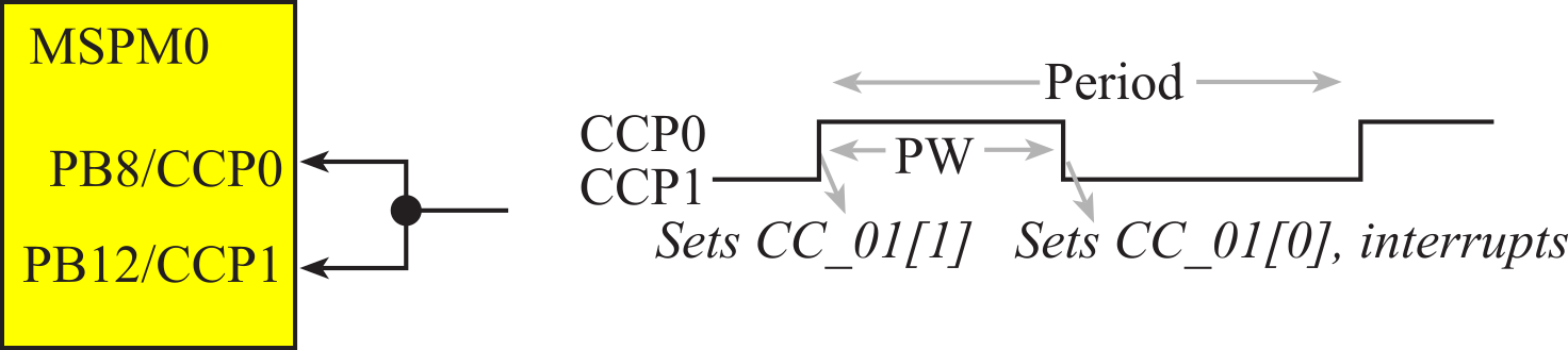
Figure M.9.3. The rising edge is measured with TIMA0_C1, and falling edge is measured with TIMA0_C0.
The pulse width measurement is performed from rising edge to falling edge. The global, PW, contains the most recent measurement. Done is set at the falling edge by the ISR signifying a new measurement is available. If the first edge after the PWMeasure_Init(); is executed is a falling edge, then the first measurement will be incorrect (because TIMA0->COUNTERREGS.CC_01[1] is incorrect). If the first edge after the PWMeasure_Init(); is executed is a rising edge, then the first measurement will be correct. Notice how little software overhead is required to perform these measurements (Program M.9.2).
uint32_t PW; // 16 bits, 1us units
int Done; // set each falling
void PWMeasure_Init(uint32_t priority){
TIMA0->GPRCM.RSTCTL = 0xB1000003;
TIMA0->GPRCM.PWREN = 0x26000001;
Clock_Delay(24); // time for TimerA0 to power up
Done = 0;
IOMUX->SECCFG.PINCM[PB8INDEX] = 0x00040084; // TIMA0 CCP0
IOMUX->SECCFG.PINCM[PB12INDEX] = 0x00040085; // TIMA0 CCP1
TIMA0->CLKSEL = 8; // 8=BUSCLK, 4= MFCLK, 2= LFCLK clock
TIMA0->CLKDIV = 0x00; // divide by 1
TIMA0->COMMONREGS.CPS = 79; // divide by 80,
TIMA0->COMMONREGS.CCPD = 0; // CCP are inputs
TIMA0->COUNTERREGS.LOAD = 0xFFFF; // set reload register
TIMA0->COUNTERREGS.CTRCTL = 0x02;
// bits 5-4 CM =0, down
// bits 3-1 REPEAT =001, continue
// bit 0 EN enable (0 for disable, 1 for enable)
TIMA0->COUNTERREGS.CCCTL_01[0] = 0x00020002; // falling edge of PB8
TIMA0->COUNTERREGS.CCCTL_01[1] = 0x00020001; // rising edge of PB12
// CCCTL_01
// bit 17 1 capture
// bits 14-12 ZCOND zero condition
// bits 10-8 LCOND load condition
// bits 6-4 ACOND advance condition
// bits 2-0 CCOND capture condition, 1 is rising, 2 is falling
TIMA0->CPU_INT.IMASK |= 0x10; // not CCD1, just CCD0 mask
TIMA0->COMMONREGS.CCLKCTL = 1;
TIMA0->COUNTERREGS.IFCTL_01[0] = 0x0002;
// bit 12 FE =0 bypass
// bit 11 CPV=0 voting
// bit 9-8 FP=00 filter period 3
// bit 7 INV=0 noninverted
// bits 3-0 =0010 input is CCP0
NVIC->ISER[0] = 1 << 18; // TIMA0 interrupt
NVIC->IP[4] = (NVIC->IP[4]&(~0x00FF0000))|(priority<<22); // set priority (bits 7,6) IRQ 18
TIMA0->COUNTERREGS.CTRCTL |= 0x01;
}
void TIMA0_IRQHandler(void){
uint32_t iidx = TIMA0->CPU_INT.IIDX;// this will acknowledge
if(iidx == 5){ // 5 means capture CCD0, PB8, TIMA0_C0
PW = (TIMA0->COUNTERREGS.CC_01[1]-TIMA0->COUNTERREGS.CC_01[0])&0xFFFF;
Done = 1;
}
}
Program M.9.2. Pulse-width measurement using two input captures.
M.10. Controller Area Network (CAN)
The fundamentals of CAN are presented in Section 9.2 This section shows the details for the MSPM0. The CAN_TX pin can be PA12 (mode 5) or PA26 (mode 6). The CAN_RX pin can be PA13 (mode 6) or PA27 (mode 6), as listed in the PINCM register. Figure M.10.1 shows the CAN interface for the ECE445M RTOS robot. This circuit exists on both sensor and motor boards. The CANH, CANL, and GND signals are connected between the boards.
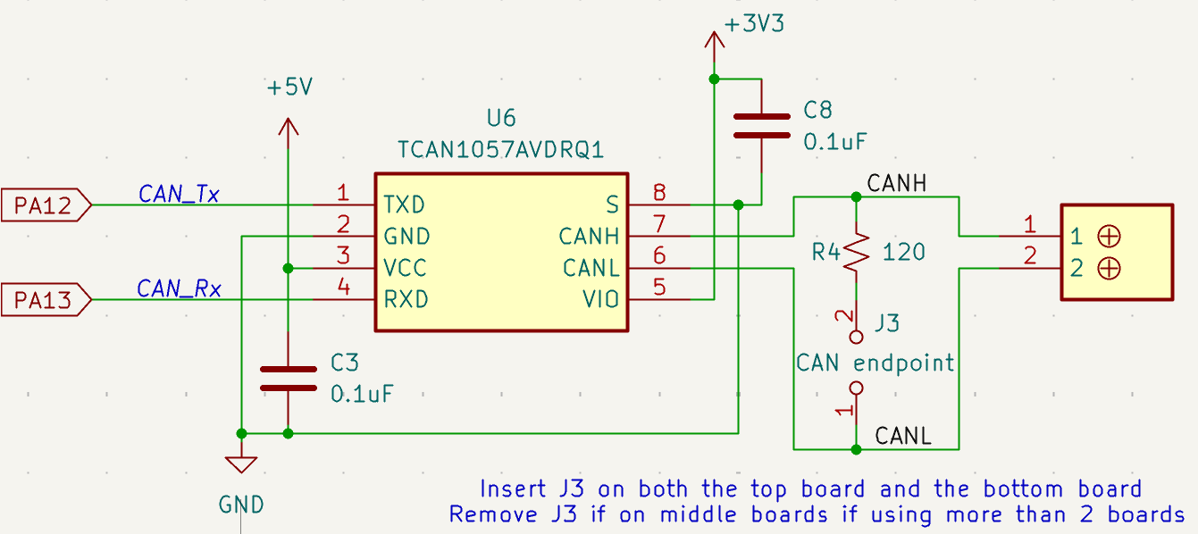
Figure M.10.1. CAN interfacing using the TCAN1057AVDRQ1 driver IC.
A device driver for the CAN network is divided into three components: initialization, transmission, and reception. There is a CAN driver available in the starter code for this book, see CAN.h and CAN.c in the inc folder and the CAN project. In this section, we will use this driver to develop a simple system that exchanges messages between two microcontrollers. Each node generates a CAN message when the S2 negative logic switch (PB21) on the LaunchPad is touched and released. There are two IDs used in this example. YourID is an 11-bit number from 0 to 1023, representing the ID of the transmitting message. TheDLC is the length of the transmitting message (0 to 8 bytes) and TheData[8] is the transmitted data. RecvID RecDLC RecvData[8] describe the received frame. The software functions on the two nodes are identical.
Transmission uses busy-wait synchronization. However, receiving messages is interrupt driven, and messages are passed from the CANFD0_IRQHandler to the user application using a second 8-deep software FIFO. The ISR will put into the FIFO, and the CAN_GetMailNonBlock function will get from the FIFO. Program M.10.1 shows the high-level user code from the CAN project.
uint32_t TheValue=0; // data values change each time
uint32_t YourID=253; // ID for transmission
uint16_t TheDLC=4; // size for transmission
uint8_t TheData[8]; // data for transmission
uint32_t RecvID,RecDLC; // received frame
uint8_t RecvData[8]; // received frame data
int main(void){
__disable_irq();
LaunchPad_Init();
Clock_Init_HFXT_40_80MHz(0);
CAN_Init();
CAN_EnableInterrupts(1); // priority=1
__enable_irq();
while(1){
if(CAN_GetMailNonBlock(&RecvID,&RecDLC,RecvData)){
GPIOB->DOUTTGL31_0 = RED;
}
if((GPIOB->DIN31_0&(1<<21))==0){// negative logic
GPIOB->DOUTTGL31_0 = GREEN;
for(int i=0; i<TheDLC; i++){
TheData[i] = TheValue++;
}
CAN_Send(YourID,TheDLC,TheData);
YourID = (YourID+1)&0x3FF; // 0 to 1023
TheDLC = (TheDLC+1)%9; // 0 to 8
while((GPIOB->DIN31_0&(1<<21))==0){
Clock_Delay(100000); // wait for release, debounce
}
}
}
}
Program M.10.1. High-level code for a simple CAN network .
This work is based on the course ECE445L
taught at the University of Texas at Austin. This course was developed by Jonathan Valvano, Mark McDermott, and Bill Bard.
Reprinted with approval from Embedded Systems: Real-Time Interfacing to ARM Cortex-M Microcontrollers, ISBN-13: 978-1463590154

Embedded Systems: Real-Time Interfacing to ARM Cortex-M Microcontrollers by Jonathan Valvano is
licensed under a Creative
Commons
Attribution-NonCommercial-NoDerivatives 4.0 International License.