9. Communication
Table of Contents:
- 9.1. Fundamentals
- 9.1.1. The network
- 9.1.2. Physical Layer
- 9.1.3. Wireless Communication
- 9.1.4. Amplitude Shift Key (ASK)
- 9.1.5. Frequency Shift Key (FSK)
- 9.1.6. Phase Shift Key (PSK)
- 9.2. Controller Area Network (CAN)
- 9.3. Communication Systems Based on UARTs
- 9.4. Bluetooth Low Energy
- 9.4.1. Fundamentals
- 9.4.2. Bluetooth Protocol Stack
- 9.4.3. Client-server Paradigm
- 9.4.4. CC2650 Microcontroller
- 9.4.5. Single Chip Solution, CC2650 LaunchPad
- 9.4.6. Network Processor Interface (NPI)
- 9.5. SubGHz Wireless
- 9.6. ZigBee Wireless
- 9.7. Lab 9 Audio Communication
The goal of this chapter is to provide a brief introduction to communication systems. Communication theory is a richly developed discipline, and much of the communication theory is beyond the scope of this book. Nevertheless, the trend in embedded systems is to employ multiple intelligent devices, therefore the interconnection will be a strategic factor in the performance of the system. These devices will be developed by different manufacturers; thus the interconnection network must be flexible, robust, and reliable. Consequently, this chapter focuses on implementing communication systems appropriate for embedded systems. The components of an embedded system are typically combined to solve a common objective, thus the nodes on the communication network will cooperate towards that shared goal. Requirements of an embedded system, in general, involve relatively low bandwidth, static configuration, and a low probability of corrupted data. We will introduce the internet of things (IoT) by designing systems that connect to the internet.
9.1. Fundamentals
9.1.1. The network
A network is a collection of interfaces that share a physical medium and a data protocol. A network allows software tasks in one computer to communicate and synchronize with software tasks running on another computer. For an embedded system, the network provides a means for distributed computing. The topology of a network defines how the components are interconnected. Example topologies using copper wire include rings, buses, and multi-drop. Figure 9.1.1 shows a ring network of four microcontrollers. The advantage of this ring network is that it is low cost and can be implemented on any microcontroller with a serial port. Notice that the microcontrollers need not be the same type or speed. The I2C protocol implements a bus network, see Figure 9.1.2, and Section 3.1.4 (I2C) .
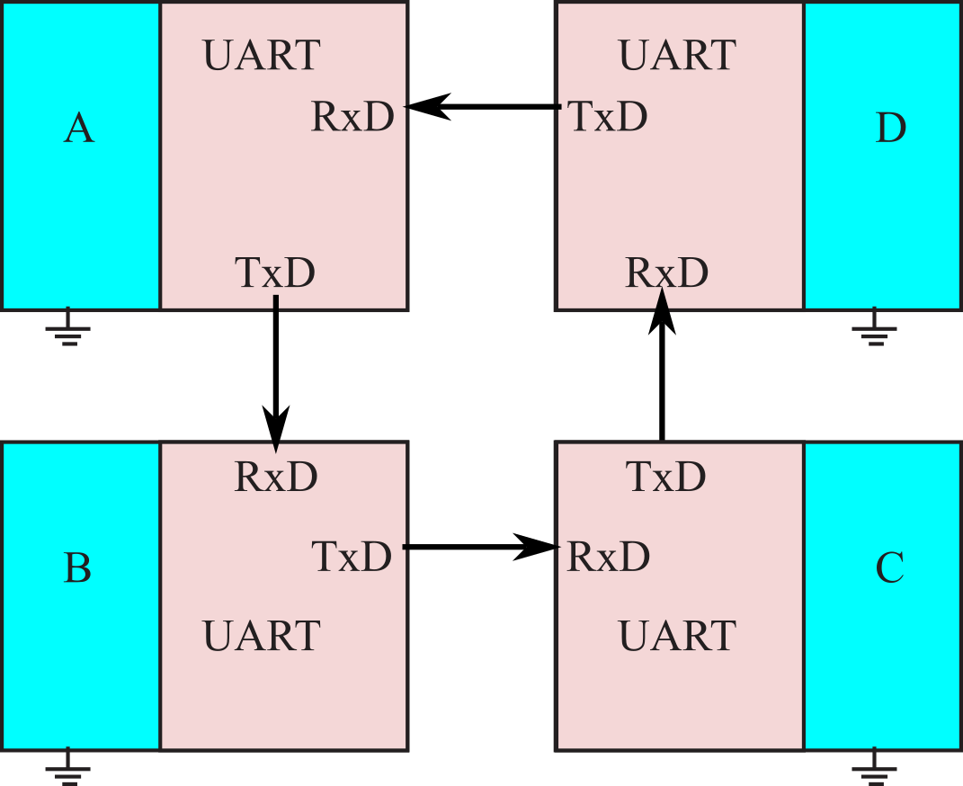
Figure 9.1.1. A simple ring network with four nodes, linked using the serial ports.
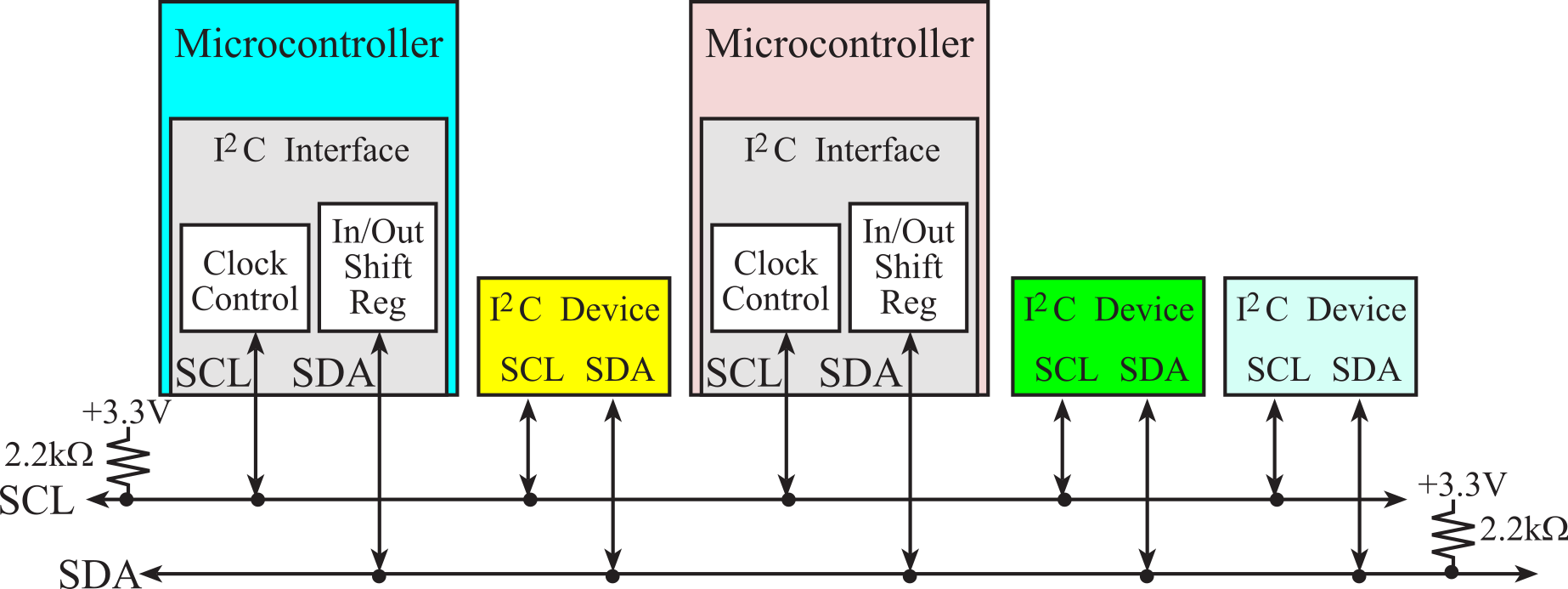
Figure 9.1.2. I2C does support communication between microcontrollers.
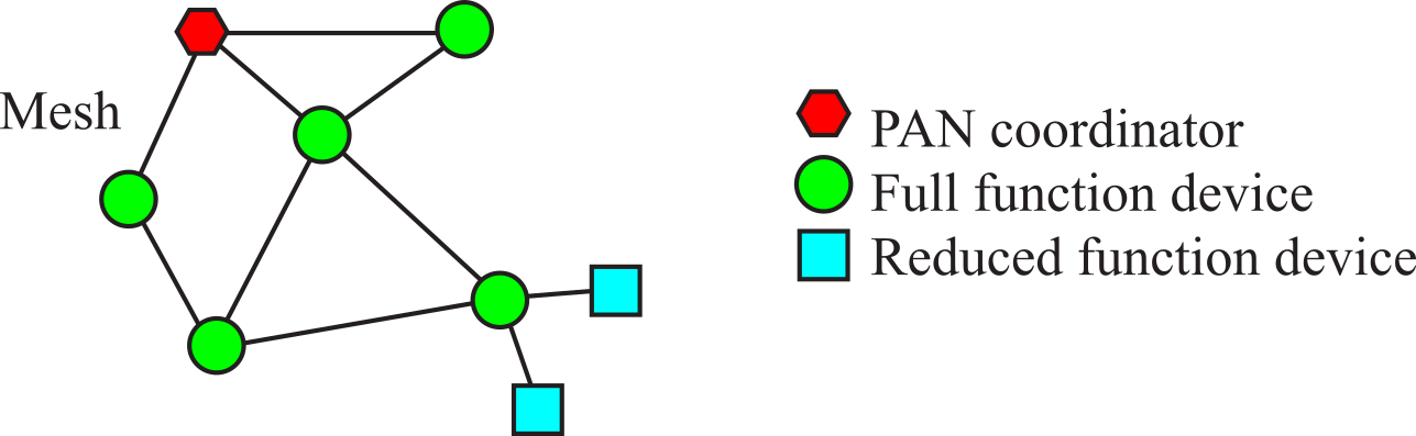
Figure 9.1.3 shows some topologies possible with radio links. The personal area network (PAN) has one coordinator, which manages the network. Personal means all nodes cooperate for a common objective. A full function device (FFD) can route messages. The reduced function device (RFD) can only receive/consume messages and create/send new messages to transmit. The star topology has a single PAN, which is connected to all other nodes. For the star and clustered tree, there is a unique routing path between any two nodes. However, with a mesh topology there can be multiple paths with which to route packets. The mesh is appropriate for mobile networks, networks that require reliability in the face of node failure, and systems that plan to grow.
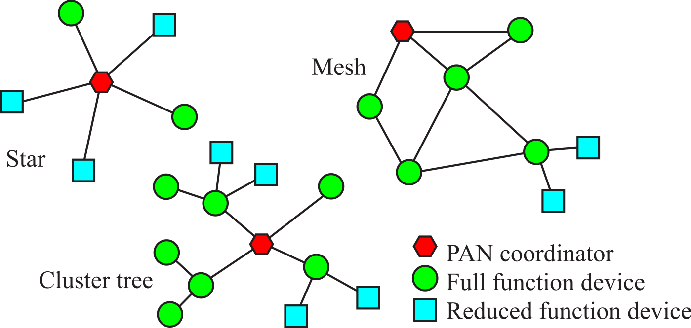
Figure 9.1.3. Wireless networks communicate by hopping between nodes.
A communication network includes both the physical channel (hardware) and the logical procedures (software) that allow users or software processes to communicate with each other across distance. The network provides the transfer of information as well as the mechanisms for process synchronization. It is convenient to visualize the network in a hierarchical fashion. Figure 9.1.4 shows the layers in a controller area network (CAN), see Section 9.2.
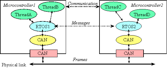
Figure 9.1.4. A layered approach to the controller area network.
Most networks provide an abstraction that hides low-level details from high-level operations. This abstraction is often described as layers. The International Standards Organization (ISO) defines a 7-layer model called the Open Systems Interconnection (OSI), as shown in Figure 9.1.5. It provides a standard way to classify network components and operations.
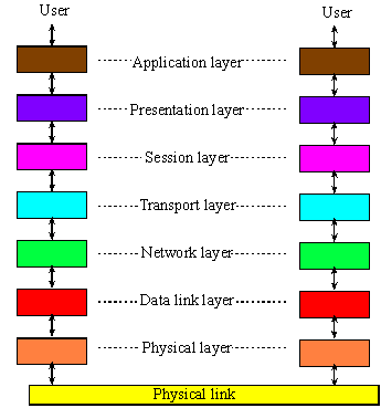
Figure 9.1.5. The Open Systems Interconnection model has seven layers.
9.1.2. Physical Layer
The Physical layer includes connectors, bit formats, and a means to transfer energy. Examples include RS232, controller area network (CAN), modem V.35, T1, 10BASE-T, 100BASE-TX, DSL, and 802.11a/b/g/n PHY. The Data link layer includes error detection and control across a single link (single hop). Examples include 802.3 (Ethernet), 802.11a/b/g/n MAC/LLC, PPP, and Token Ring. The Network layer defines end-to-end multi-hop data communication. The Transport layer provides connections and may optimize network resources. The Session layer provides services for end-user applications such as data grouping and check points. The Presentation layer includes data formats, transformation services. The Application layer provides an interface between network and end-user programs.
Observation: Communication systems often specify bandwidth in total bits/sec, but the important parameter is the data transfer rate.
Observation: Often the bandwidth is limited by the software and not the hardware channel.
Many embedded systems require the communication of command or data information to other modules at either a near or a remote location. A full duplex channel allows data to transfer in both directions at the same time. Ethernet, SPI, and UART implement full duplex communication. In a half duplex system, data can transfer in both directions but only in one direction at a time. Half duplex is popular because it is less expensive and allows the addition of more devices on the channel without change to the existing nodes. CAN, I2C, and most wireless protocols implement half-duplex communication. A simplex channel allows data to flow in only one direction.
: In which manner to most people communicate: simplex, half duplex or full duplex?
Information, such as text, sound, pictures and movies, can be encoded in digital form and transmitted across a channel, as shown in Figure 9.1.6. Channel capacity is defined as the maximum information per second it can transmit. To improve the capacity, many communication systems will compress the information at the source, transmit the compressed version, and then decompress the data at the destination. Compression essentially removes redundant information in such a way that the decompressed data is identical (lossless) or slightly altered but similar enough (lossy). For example, a 400 pixels/inch photo compressed using the JPEG algorithm will be 5 to 30 times smaller than the original.
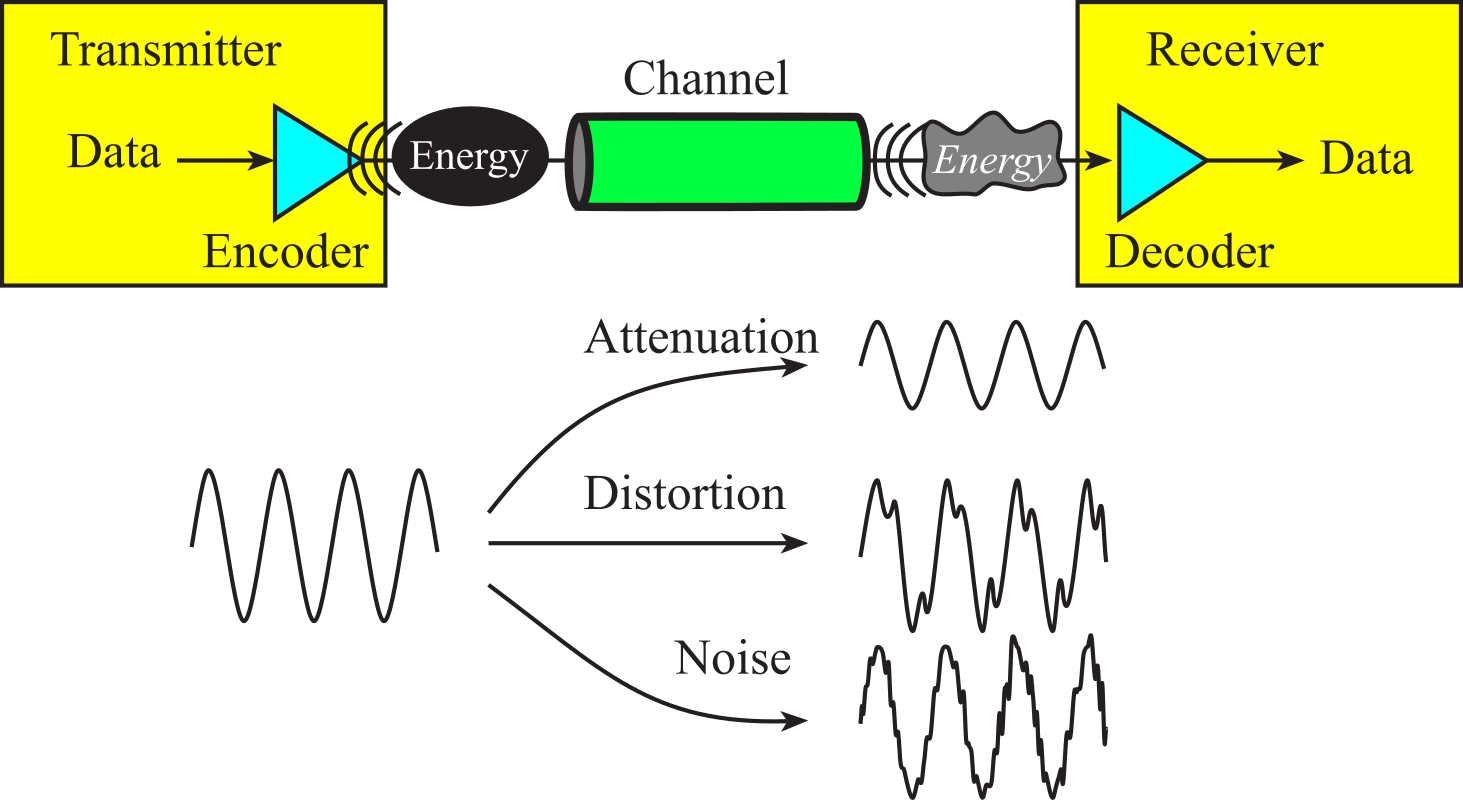
Figure 9.1.6. Information is encoded as energy, and errors can occur during transmission.
In general, for communication to occur, the transmitter must encode information as energy, the channel must allow the energy to move from transmitter to receiver, and the receiver must decode the energy back into the information, see Figure 9.1.6. In an analog communication system, energy can vary continuously in amplitude and time. AM radio is an example of analog communication. A digital communication signal exists at a finite number of energy levels for discrete amounts of time.
A guided medium focuses the transmission of energy into a well-defined path, such as current flowing along copper wire of a twisted pair cable, or light traveling along a fiber optic cable. Conversely, an unguided medium has no focus, and the energy field diffuses as in propagates, such as sound or EM fields in air or water.
Along the way, the energy may be lost due to attenuation. For example, a simple V=I*R voltage drop is a loss of energy as electrical energy converted to thermal energy. A second example of attenuation is an RF cable splitter. For each splitter, there will be 50% attenuation, where half the energy goes left and the other half goes right through the splitter. Unguided media will have attenuation as the energy propagates in multiple directions. Attenuation causes the received energy to be lower in amplitude than the transmitted energy.
A second problem is distortion. The transfer gain and phase in the channel may be function of frequency, time, or amplitude. Distortion causes the received energy to have a different shape than the transmitted energy. Signals traveling down a copper wire are distorted by the capacitance of the cable.
A third problem is noise. The noise energy is combined with the information energy to create a new signal. White noise is an inherent or internally generated noise caused by thermal fluctuations. EM field noise is externally generated and is coupled or added into the system. Crosstalk is a problem where energy in one wire causes noise in an adjacent wire. We quantify noise with signal-to-noise ratio (SNR), which is the ratio of the information signal power to noise power.
![]()
: Why do we measure SNR as power and not voltage?
: Why do we always have a ratio of two signals whenever we use the log10 to calculate the amplitude of a signal?
Observation: Whenever we use the log10 to calculate the amplitude of a signal, we multiply by 10 if we have a ratio of two power signals or energy signals, and we multiply by 20 if we have a ratio of two voltage signals or current signals.
We can make an interesting analogy between time and space. A communication system allows us transfer information from position A to position B. A digital storage system allows us transfer information from time A to time B. Many of the concepts (encoding/decoding information as energy, signal to noise ratio, error detection/correction, security, and compression) apply in an analogous manner to both types of systems.
: We measure the performance of a communication system as bandwidth in bits/sec. What is the analogous performance measure of a digital storage system?
Errors can occur when communicating through a channel with attenuation, distortion and added noise. If the receiver detects an error, it can send a negative acknowledgement so the transmitter will retransmit the data. The CAN, ZigBee, and Bluetooth protocols handle this detection-retransmission process automatically. Networks based on the UARTs could define and implement error detection. For example, we can add an additional bit to the serial frame for the purpose of detecting errors. With even parity, the sum of the data bits plus the parity bit will be an even number. The framing error in the UART can also be used to signify the data may be corrupted. The CAN network sends a longitudinal redundancy check, LRC, which is the exclusive or of the bytes in the frame. The ZigBee network adds a checksum, which is the sum of all the data. The Network Processor Interface (NPI) later in this chapter uses LRC.
There are many ways to improve transmission in the channel, reducing the probability of errors. The first design choice is the selection of the interface driver. For example, a UART with RS422 is less likely to exhibit errors than a UART with RS232. Of course, having a driver will be more reliable than not having a driver. The second consideration is the cable. Proper shielding can improve SNR. For example, Cat6 Ethernet cables have a separator between the four pairs of twisted wire, which reduces the crosstalk between lines as compared to Cat5e cable. If we can separate or eliminate the source of added noise, the SNR will improve. Reducing the distance and reducing the bandwidth often will reduce the probability of error. If we must transmit long distances, we can use a repeater, which accepts the input and retransmits the data again.
Error correcting codes are beyond the scope of this book. However, we can present two simple error correcting codes. The first error correcting code involves sending three copies of each data. The receiver will compare the three versions received and the majority vote will decide which value to use.
A second error correcting code uses both parity and LRC. For example, assume we wished to send the message "Ciao". Encoded as ASCII characters the data are 0x43, 0x69, 0x61, and 0x6F. The first step is to visualize the binary data in 2-D.
|
|
Byte 0 |
Byte 1 |
Byte 2 |
Byte 3 |
|
Bit 7 |
0 |
0 |
0 |
0 |
|
Bit 6 |
1 |
1 |
1 |
1 |
|
Bit 5 |
0 |
1 |
1 |
1 |
|
Bit 4 |
0 |
0 |
0 |
0 |
|
Bit 3 |
0 |
1 |
0 |
1 |
|
Bit 2 |
0 |
0 |
0 |
1 |
|
Bit 1 |
1 |
0 |
0 |
1 |
|
Bit 0 |
1 |
1 |
1 |
1 |
The second step is to add an even parity bit to each byte and add a 9-bit LRC at the end.
|
|
Byte 0 |
Byte 1 |
Byte 2 |
Byte 3 |
LRC |
|
Parity |
1 |
0 |
1 |
0 |
0 |
|
Bit 7 |
0 |
0 |
0 |
0 |
0 |
|
Bit 6 |
1 |
1 |
1 |
1 |
0 |
|
Bit 5 |
0 |
1 |
1 |
1 |
1 |
|
Bit 4 |
0 |
0 |
0 |
0 |
0 |
|
Bit 3 |
0 |
1 |
0 |
1 |
0 |
|
Bit 2 |
0 |
0 |
0 |
1 |
1 |
|
Bit 1 |
1 |
0 |
0 |
1 |
0 |
|
Bit 0 |
1 |
1 |
1 |
1 |
0 |
Notice that the even parity is the exclusive OR of each bit in the vertical column and the LRC is the exclusive OR of each bit in the horizontal row. The parity bit for the LRC (or the LRC bit for the parity) will be the exclusive OR of all the data bits.
Now, if any one bit in this 9-row by 5-column matrix is flipped, we can determine which byte is in error by the parity and which bit is in error by the LRC. Rather than asking for retransmission, we simply correct the error. These are very simple error correcting codes, but they illustrate that we can send more bits than the minimum and use those extra bits in a creative way to either detect or correct errors.
RS422, RS485, Ethernet, and CAN are high-speed communication channels. This means the bandwidth and slew rate on the signals are higher than RS232. There is a correspondence between rise time (t) of a digital signal and equivalent sinusoidal frequency (f). The derivative of A*sin(2πft) is 2πf*A*cos(2πft). The maximum slew rate of this sinusoid is 2πf*A. Approximating the slew rate as A/t, we get a correspondence between f and t
f = 1/t
For example, if the rise time is 5 ns, the equivalent frequency is 200 MHz. Notice that this equivalent frequency is independent of baud rate. So, even at 1000 bits/sec, if the rise time is 5 ns, then the signal has a strong 200 MHz frequency component! To deal with this issue, the RS232 protocol limits the slew rate to a maximum of 30V/µs. This means it will take about 400 ns for a signal to rise from -6 to +6 V. Consequently, RS232 signals have frequency components less than 2 MHz. However, to transmit faster than RS232, the protocol must have faster rise times. Electrical signals travel at about 0.6 to 0.9 times the speed of light. This velocity factor (VF) is a property of the cable. For example, VF for RG-6/U coax cable is 0.75, whereas VF is only 0.66 for RG-58/U coax cable. Using the slower 0.66 estimate, the speed is v = 2*108 m/s. According to wave theory, the wavelength is l = v/f. Estimating the frequency from rise time, we get
l = v * t
In our example, a rise time of 5 ns is equivalent to a wavelength of about 1 m. As a rule of thumb, we will consider the channel as a transmission line if the length of the wire is greater than l/4, which is 25 cm for this signal with a 5-ns rise time. Another requirement is for the diameter of the wire to be much smaller than the wavelength. In a transmission line, the signals travel down the wires as waves according to the wave equation. Analysis of the wave equation is outside the scope of this book. However, you need to know that when a wave meets a change in impedance, some of the energy will transmit (a good thing) and some of the energy will reflect (a bad thing). Reflections are essentially noise on the signal, and if large enough, they will cause bit errors in transmission. We can reduce the change in impedance by placing terminating resistors on both ends of a long high-speed cable, which are needed for both CAN and Ethernet. These resistors reduce reflections; hence they improve signal to noise ratio.
: What is the ¼ wavelength distance if the rise time is 100ns?
9.1.3. Wireless Communication
The details of exactly how wireless communication operates are beyond the scope of this book. Nevertheless, the interfacing techniques presented in this book are sufficient to implement wireless communication by selecting a wireless module and interfacing it to the microcontroller. In general, one considers bandwidth, distance, topology and security when designing a wireless link. Bandwidth is the fundamental performance measure for a communication system. In this book, we define bandwidth of the system as the information transfer rate. However, when characterizing the physical channel, bandwidth can have many definitions. In general, the bandwidth of a channel is the range of frequencies passed by the channel (Communication Networks by Leon-Garcia). Let Gx(f) be the gain versus frequency of the channel. When considering EM fields transmitted across space, we can define absolute bandwidth as the frequency interval that contains all the signal's frequencies. Half-power bandwidth is the interval between frequencies at which Gx(f) has dropped to half power (‑3dB). Let fc be the carrier frequency, and Px be the total signal power over all frequencies. The equivalent rectangular bandwidth is Px/Gx(fc). The null-to-null bandwidth is the frequency interval between first two nulls of Gx(f). The FCC defines fractional power containment bandwidth as the bandwidth with 0.5% of signal power above and below the band. The bounded power spectral density is the band defined so that everywhere outside Gx(f) must have fallen to a given level. The purpose of this list is to demonstrate to the reader that, when quoting performance data, we must give both definition of the parameter and the data. If we know the channel bandwidth W in Hz and the SNR, we can use the Shannon-Hartley Channel Capacity Theorem to estimate the maximum data transfer rate C in bits/s:
![]()
For example, consider a telephone line with a bandwidth W of 3.4 kHz and SNR of 38 dB. The dimensionless SNR = 10(38/10) = 6310. Using the Channel Capacity Theorem, we calculate C = 3.4 kHz * log2(1 + 6310) = 43 kbits/s.
Figure 9.1.7 shows a rough image of various electromagnetic waves that exist from radio waves to gamma rays. Visible light constitutes a very small fraction, ranging from 430-770 THz. Bluetooth. ZigBee, and WiFi use an even narrower range from 2.40 to 2.48 GHz, which exists in the microwave spectrum.
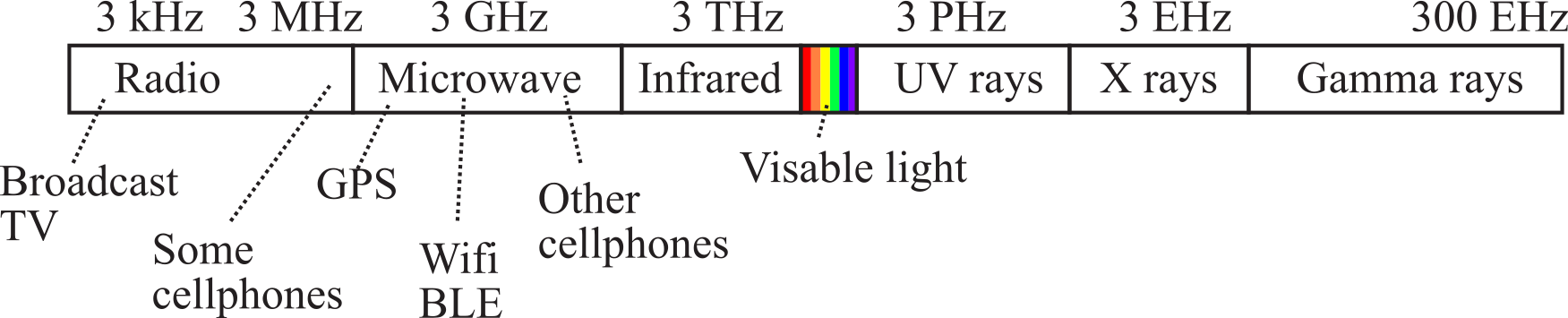
Figure 9.1.7. Bluetooth communication occurs in the microwave band at about 2.4 GHz.
Table 9.1.1 shows some general descriptions of the three major communication standards operating in this 2.4 GHz band.
|
Standard |
Description |
|
WiFi |
Up to 600 Mbits/sec |
|
Bluetooth/BLE |
Very low power |
|
ZigBee |
Very low power |
Table 9.1.1. Comparison between Wi-Fi, Bluetooth, and ZigBee.
9.1.4. Amplitude Shift Key (ASK)
One of the simplest encode-decode schemes is amplitude shift key (ASK). In ASK, the binary information is encoded as amplitudes. If one of the amplitudes is 0, and other is nonzero, we call it on-off key (OOK), as shown in Figure 9.1.8.
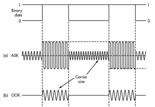
Figure 9.1.8. On-off key is an example of amplitude shift key.
To send ASK, the transmitter has a high frequency periodic interrupt that outputs a sinewave. Let Bit be a global variable which is 1 (for small amplitude) and 0 (for large amplitude). Let the carrier frequency be fc=1kHz, which will be fixed. If N is size of the buffer, the periodic interrupt rate should be N*fc. If N=16, the high frequency interrupt is 16 kHz.
Fetch one DAC value from a buffer
Output that value>>Bit to the DAC
Increment the index by 1, and wrap the index back to 0 if needed
Notice there are 8 waves/bit in Figure 9.1.8a, so each bit takes 8ms, making the baud rate 125 bits/sec. Let f be the desired baud rate. We need a second periodic interrupt executing at f. We will use a bit FIFO to pass data from system to the transmitter. This means we put and get one bit at a time. The system stores the desired message as a bit stream by putting bits into the FIFO.
Get one data bit from a FIFO
If the FIFO was empty, set Bit=16 (no sound)
If the data bit is 0, set Bit=1 (50% amplitude)
If the data bit is 1, set Bit=0 (100% amplitude)
To send a frame, we will need a start bit (data=0, bit=1, 50% amplitude). Figure 9.1.9 shows a 10-bit ASK frame (1kHz, 125 bits/sec) as it is sampled at the receiver.
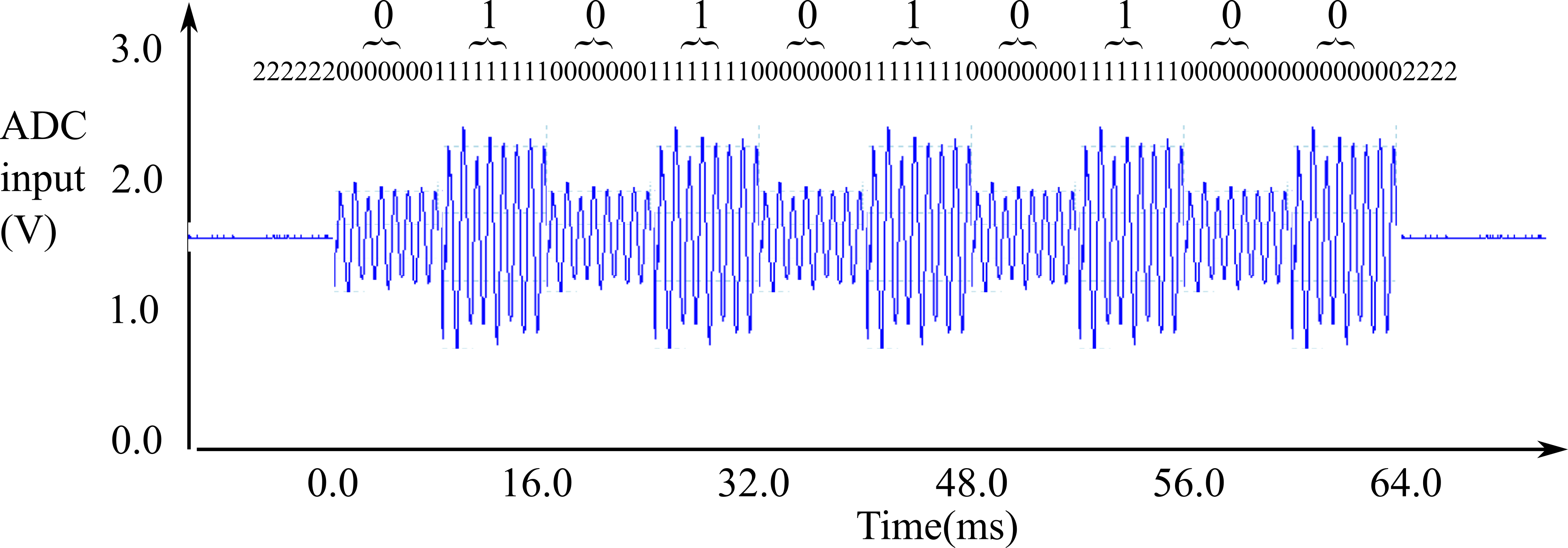
Figure 9.1.9. Ten bit frame of amplitude shift key as it is decoded by the receiver.
In this simple example, let the average input be 2048 because there is an analog HPF. To detect a start of frame we will sample the input until we have an input large enough to constitute a transmission. A simple measure of amplitude is RMS (without the square root). The threshold variable is set to halfway between low and high. We can determine if the audio input signal is large or small by calculating RMS (without the square root) and comparing it to the threshold. This 16 kHz ISR puts into one bit FIFO every 1 ms
x = Sample ADC
ACsum = (x-2048)2
I = I+1
if I is 16 is 0{
if(ACsum > threshold){
put(1) // high
}else{
if(ACsum > threshold/4){
put(0) // low
}
else{
put(2) // no bit
}
}
ACsum=0 and I=0
}
Since the bit time is 8ms, we can expect the bit FIFO to contain 8 0's for each data bit of 0, and 8 1's for each data bit of 1.
9.1.5. Frequency Shift Key (FSK)
Figure 9.1.10 shows a simple frequency shift key encoding. For this protocol, a 1 kHz audio signal means 1, and the 2 kHz audio signal means 0. The bit time in this example is 10ms, so the baud rate is 100 Hz.
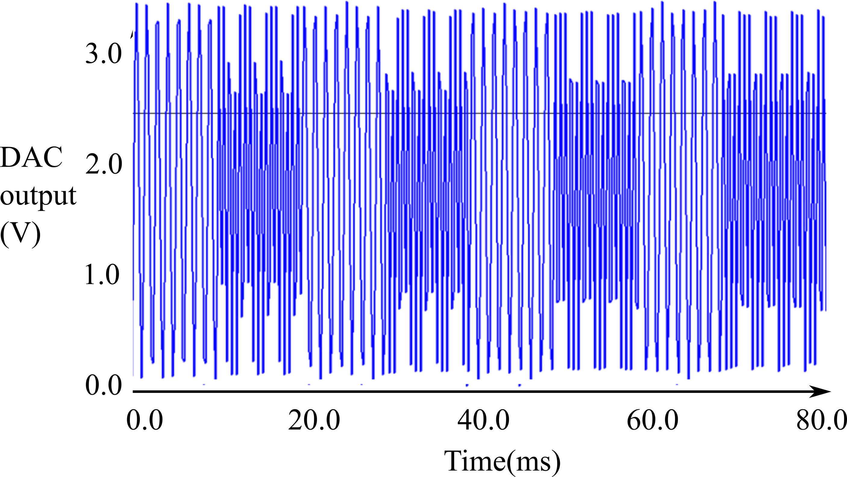
Figure 9.1.10. Frequency shift key implemented with audio tones.
To send this signal, the transmitter has a high frequency periodic interrupt that outputs a sinewave. Let Bit be a global variable which is 1 (for 1 kHz) and 2 (for 2 kHz). If N is size of the buffer, the periodic interrupt rate should be N kHz. For the data shown in Figure 9.1.10, the baud rate is 100 Hz, N=16, so the high frequency interrupt is 16 kHz.
Fetch one DAC value from a buffer
Output that value to the DAC
Increment the index by Bit, and wrap the index back to 0 if needed
Let f be the desired baud rate. We need a second periodic interrupt executing at f. We will use a bit FIFO to pass data from system to the transmitter. This means we put and get one bit at a time. The system stores the desired message as a bit stream by putting bits into the FIFO.
Get one data bit from a FIFO
If the FIFO was empty, set Bit=0 (no sound)
If the data bit is 0, set Bit=2 (2 kHz)
If the data bit is 1, set Bit=1 (1 kHz)
In Figure 9.1.11 the baud rate is 100 bits/sec. Every 10ms, a new bit is sent. This figure shows a 10-bit frame, with start bit, 8 data bits and even parity. The format for this message is
Start, B0, B1, B2, B3, B4, B5, B6, B7, Parity
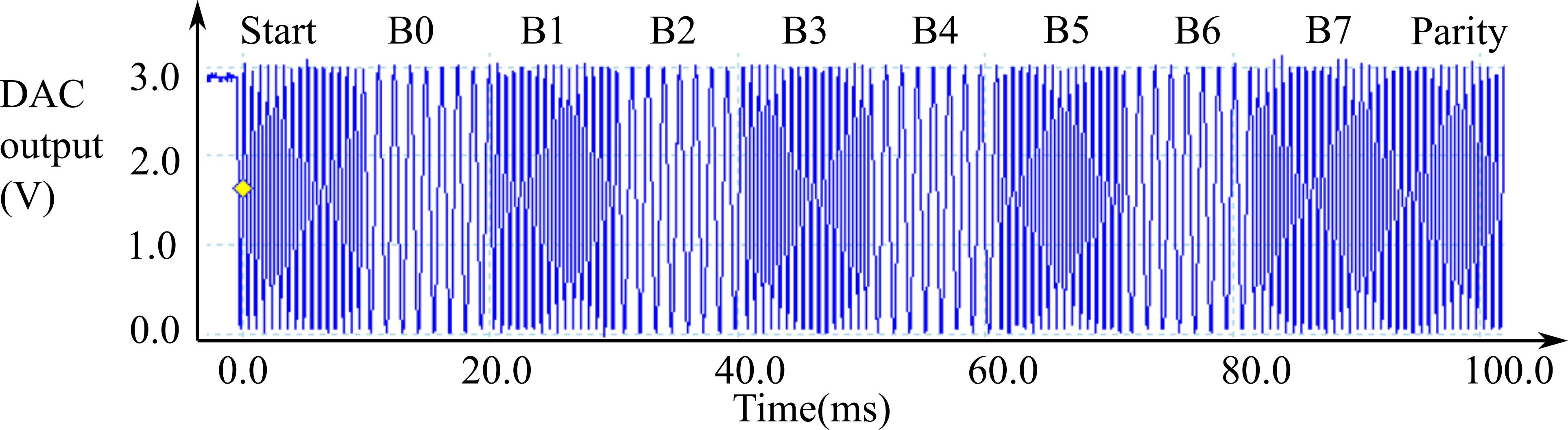
Figure 9.1.11. 10-bit transmission using a simple FSK protocol, ASCII 'U' 0x55.
Decoding this protocol is much harder than encoding. One way to determine if the audio input signal is 1 kHz or 2 kHz is to use the Discrete Fourier Transform (DFT). If we sample the input at 16 kHz, the k=1 term of the DFT represents 1 kHz and the k=2 term of the DFT represents 2 kHz. The 16 kHz periodic interrupt samples the ADC and accumulates DFT calculations. See M.5 Discrete Fourier Transform for the details of the DFT.
a = Sample ADC
rsum1 += a*ReW[i]
isum1 += a*ImW[i]
rsum2 += a*ReW[2*i]
isum2 += a*ImW[2*i]
The 1 kHz periodic interrupt performs the k=1 and k=2 DFT and decide if the input is 1 kHz, 2 kHz or neither. The shift right prevents the calculation from overflowing the 32-bit processor. Encoding also uses a bit FIFO. Because the DFT occurs every 1ms, and the bit time is 10ms, we can expect 9, 10, or 11 bits of DFT output for every data bit.
mag1 = (rsum1>>10)*(rsum1>>10)+(isum1>>10)*(isum1>>10)
mag2 = (rsum2>>10)*(rsum2>>10)+(isum2>>10)*(isum2>>10)
if mag1 is high and mag2 is low, put(1)
else if mag2 is high and mag1 is low, put(0)
else put(2)
Clear all four sums
Figure 9.1.12 shows an ADC input data, with the corresponding bit stream created by the 1 kHz periodic interrupt. Another thread gets from this bit FIFO and converts the bit stream into data.
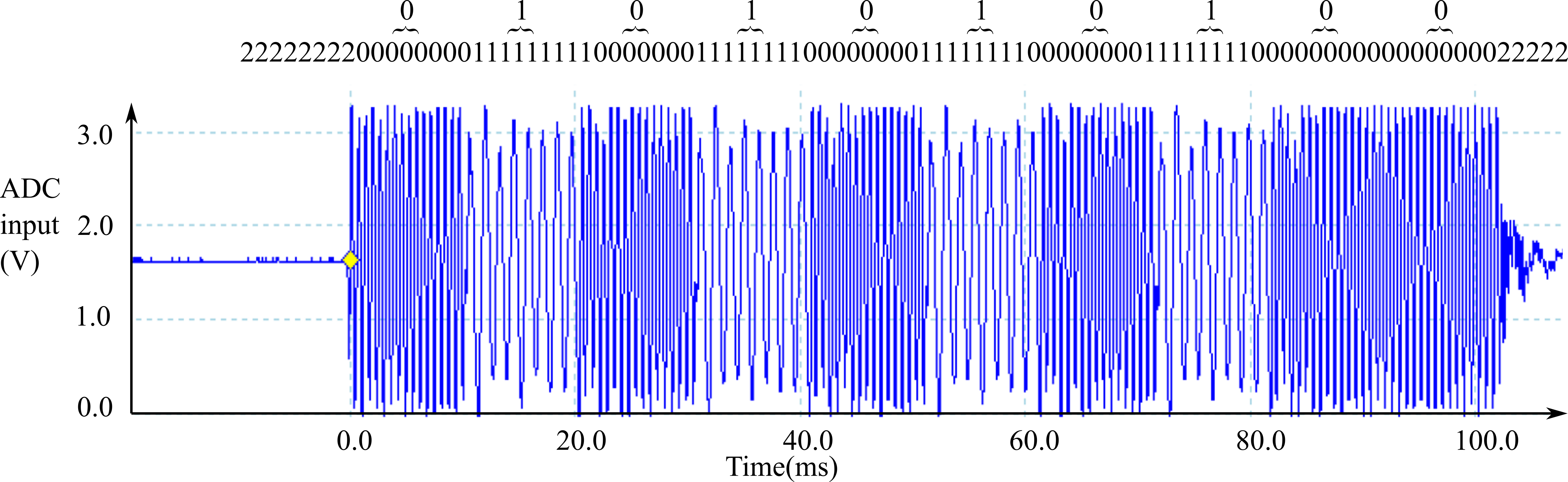
Figure 9.1.12. Encode this simple FSK using DFT.
Just like a UART decoder, we can look for the 222000 sequence and set the start of the frame at between the 222 and the 000. Let T=10ms be the bit time of the protocol. Next, we observe three DFT bits at ½*T, 1½*T, ... 9½*T. These three bits to be equal for a valid communication. If they are not equal, the communication is invalid.
: How would the decoding change if the receiver samples at 32 kHz?
9.1.6. Phase Shift Key (PSK)
The next decode-encode scheme we will present is phase shift key (PSK), as illustrated in Figure 9.1.13. Let the carrier frequency be fc=433 MHz, which will be fixed. In this scheme, the binary information is encoded as 0 and 180 degree phase.
Binary 0 s(t) = A cos(2πfc t+ π) = -A cos(2πfc t)
Binary 1 s(t) = A cos(2πfc t)
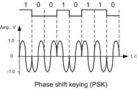
Figure 9.1.13. Phase shift key.
To send PSK, the transmitter has a high frequency task that outputs a sinewave. At 433 MHz, this task must be mixed analog/digital hardware, not software. If N is size of the buffer, the high frequency task executes at N*fc. If N=16, the high frequency task runs at 6.928 GHz. Let Index be the index into the sinewave buffer (0≤Index≤15).
Fetch one DAC value from a buffer
Output that value to the DAC
Index = (Index+1)&(N-1)
Let f be the desired baud rate. We need a second periodic task executing at f. We will use a bit FIFO to pass data from system to the transmitter. This means we put and get one bit at a time. The system stores the desired message as a bit stream by putting bits into the FIFO. For this simple example, we encode 0 as phase=+180 and 1 as phase=0.
Get one data bit from a FIFO
If the FIFO was empty, we turn off the radio to save power
If the data bit is 0, set Index = N/2 (+180 phase)
If the data bit is 1, Index = 0 (0 phase)
To decode this protocol we could use M.5 Discrete Fourier Transform (DFT) or M.5. Cross Correlation, both of which contain phase information. However, the fastest decoding uses this trig identity.
sin(2πfct+θ1)*sin(2πfct+θ2)=½[cos(θ1-θ2)-cos(4πfct+(θ1+θ2))]
One wave (sin(2πfct+θ1)) is the sampled input, and the other (sin(2πfct+θ2)) is a known template. An analog multiplier, followed by a LPF, gives a continuous output of the phase of the received signal.
½ cos(θ1-θ2)
For more information see, https://en.wikipedia.org/wiki/Phase-shift_keying
9.2. Controller Area Network (CAN)
In this section, we will design and implement a Controller Area Network (CAN). CAN is a high-integrity serial data communications bus that is used for real-time applications. It can operate at data rates of up to 1 Mbits/second, having excellent error detection and confinement capabilities. The CAN was originally developed by Robert Bosch for use in automobiles, and is now extensively used in industrial automation and control applications. The CAN protocol has been developed into an international standard for serial data communication, specifically the ISO 11989.
Figure 9.2.1 shows the block diagram of a CAN system, which can have up to 112 nodes. There are four components of a CAN system. The physical channel is the CAN bus consisting of two wires (CANH, CANL) with 120-Ω termination resistors on each end. The physical layer also includes an integrated circuit called the Transceiver, which handles the voltage levels and interfacing the separate receive (RxD) and transmit (TxD) signals onto the CAN bus. The data link layer includes the CAN controller, which is hardware built into the microcontroller, and it handles message timing, priority, error detection, and retransmission. The network layer includes software that handles the high-level functions of generating data to transmit and processing data received from other nodes.
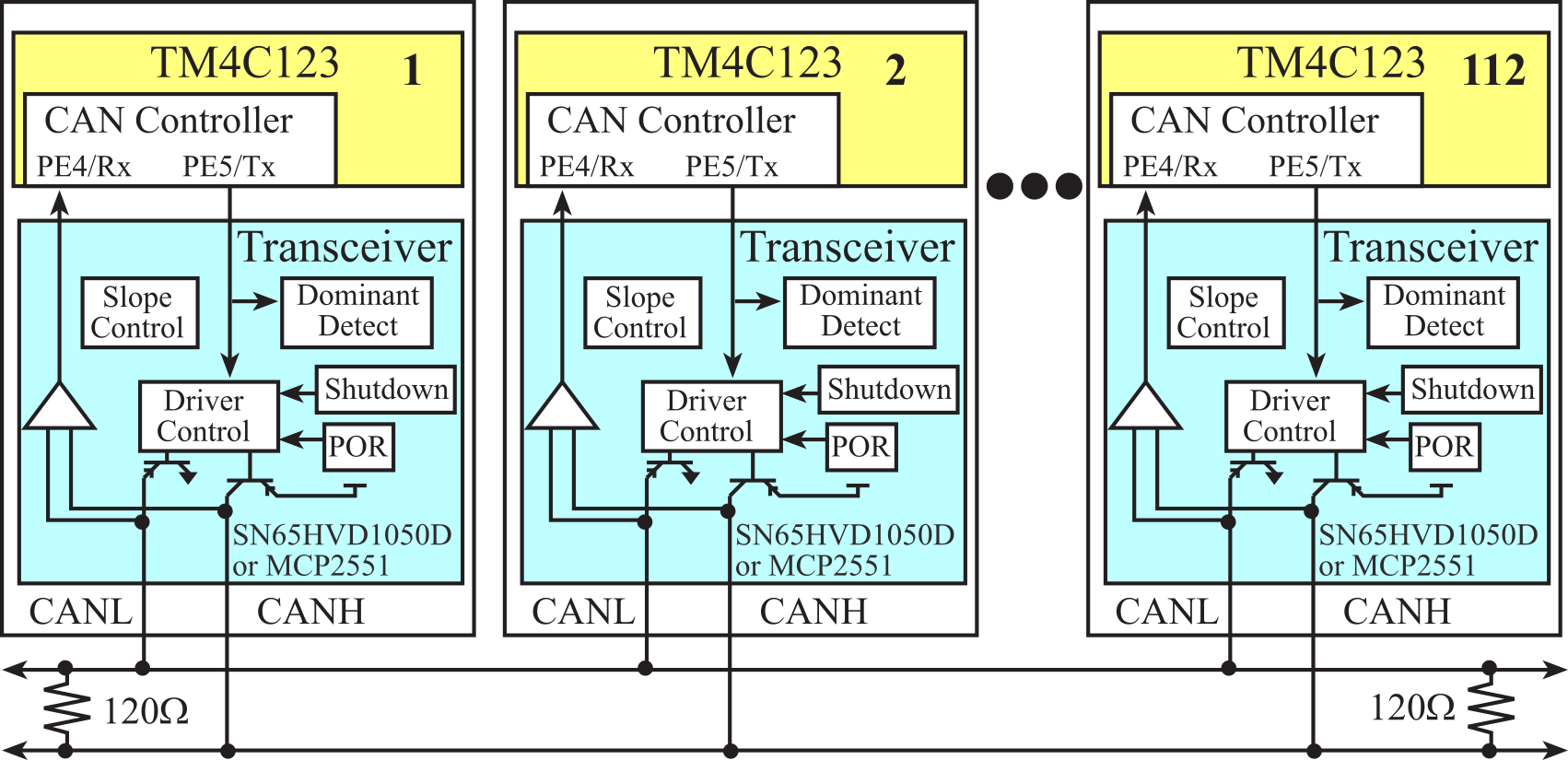
Figure 9.2.1. Block Diagram of a TM4C-Based CAN communication system
Each node consists of a microcontroller (with an internal CAN controller), and a transceiver that interfaces the CAN controller to the CAN bus. A transceiver is a device capable of transmitting and receiving on the same channel. The CAN is based on the "broadcast communication mechanism", which follows a message-based transmission protocol rather than an address-based protocol. The CAN provides two communication services: the sending of a message (data frame transmission) and the requesting of a message (remote transmission request). All other services such as error signaling, automatic retransmission of erroneous frames are user-transparent, which implies that the CAN interface automatically performs these functions. The TM4C123 has two CAN devices. The MSPM0G3507 has one CAN device. The physical channel consists of two wires containing in differential mode one digital logic bit. Because multiple outputs are connected together, there must be a mechanism to resolve simultaneous requests for transmission. In a manner similar to open collector logic, there are dominant and recessive states on the transmitter, as shown in Figure 9.2.2. The outputs follow a wired-and mechanism in such a way that if one or more nodes are sending a dominant state, it will override any nodes attempting to send a recessive state.
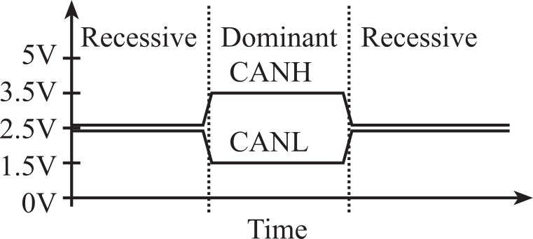
Figure 9.2.2. Voltage specifications for the recessive and dominant states.
: What are the dominant and recessive states in open collector logic?
The CAN transceiver is a high-speed, fault-tolerant device that serves as the interface between a CAN protocol controller (located in the microcontroller) and the physical bus. The transceiver is capable of driving the large current needed for the CAN bus and has electrical protection against defective stations. Typically, each CAN node must have a device to convert the digital signals generated by a CAN controller to signals suitable for transmission over the bus cabling. The transceiver also provides a buffer between the CAN controller and the high-voltage spikes than can be generated on the CAN bus by outside sources. Examples of CAN transceiver chips include the Texas Instruments SN65HVD1050D, AMIS-30660 high speed CAN transceiver, ST Microelectronics L9615 transceiver, Philips Semiconductors AN96116 transceiver, and the Microchip MCP2551 transceiver. These transceivers have similar characteristics and would be equally suitable for implementing a CAN system.
In a CAN system, messages are identified by their contents rather by addresses. Each message sent on the bus has a unique identifier, which defines both the content and the priority of the message. This feature is especially important when several stations compete for bus access, a process called bus arbitration. As a result of the content-oriented addressing scheme, a high degree of system and configuration flexibility is achieved. It is easy to add stations to an existing CAN network.
Four message types or frames can be sent on a CAN bus. These include the Data Frame, the Remote Frame, the Error Frame, and the Overload Frame. This section will focus on the Data Frame, where the parts in standard format are shown in Figure 9.2.3. The Arbitration Field determines the priority of the message when two or more nodes are contending for the bus. For the Standard CAN 2.0A, it consists of an 11-bit identifier. For the Extended CAN 2.0B, there is a 29-bit Identifier. The identifier defines the type of data. The Control Field contains the DLC, which specifies the number of data bytes. The Data Field contains zero to eight bytes of data. The CRC Field contains a 15-bit checksum used for error detection. Any CAN controller that has been able to correctly receive this message sends an Acknowledgement bit at the end of each message. This bit is stored in the Acknowledge slot in the CAN data frame. The transmitter checks for the presence of this bit and if no acknowledge is received, the message is retransmitted. To transmit a message, the software must set the 11-bit Identifier, set the 4-bit DLC, and give the 0 to 8 bytes of data. The receivers can define filters on the identifier field, so only certain message types will be accepted. When a message is received the software can read the identifier, length, and data.
The Intermission Frame Space (IFS) separates one frame from the next. There are two factors that affect the number of bits in a CAN message frame. The ID (11 or 29 bits) and the Data fields (0, 8, 16, 24, 32, 40, 48, 56, or 64 bits) have variable length. The remaining components (36 bits) of the frame have fixed length including SOF (1), RTR (1), IDE/r1 (1), r0 (1), DLC (4), CRC (15), and ACK/EOF/intermission (13). For example, a Standard CAN 2.0A frame with two data bytes has 11+16+36 = 63 bits. Similarly, an Extended CAN 2.0B frame with four data bytes has 29+32+36 = 97 bits.
If a long sequence of 0's or a long sequence of 1's is being transferred, the data line will be devoid of edges that the receiver needs to synchronize its clock to the transmitter. In this case, measures must be taken to ensure that the maximum permissible interval between two signal edges is not exceeded. Bit Stuffing can be utilized by inserting a complementary bit after five bits of equal value. Some CAN systems add stuff bits, where the number of stuff bits depends on the data transmitted. Assuming n is the number of data bytes (0 to 8), CAN 2.0A may add 3+n stuff bits and a CAN 2.0B may add 5+n stuff bits. Of course, the receiver has to un-stuff these bits to obtain the original data.
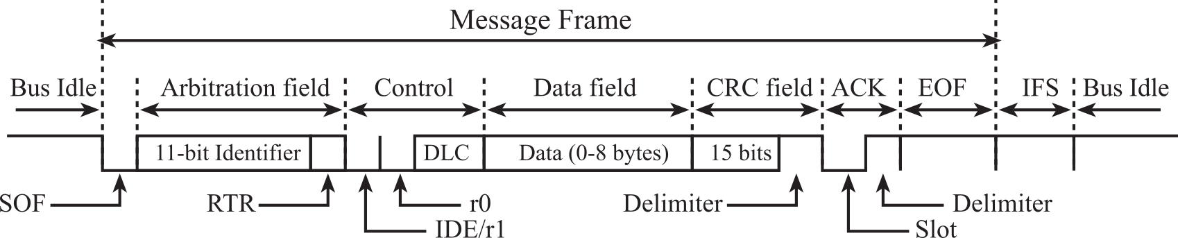
Figure 9.2.3. CAN Standard Format Data Frame.
The urgency of messages to be transmitted over the CAN network can vary greatly in a real-time system. Typically, there are one or two activities that require high transmission rates or quick responses. Both bandwidth and response time are affected by message priority. Low priority messages may have to wait for the bus to be idle. There are two priorities occurring as the CANs transmit messages. The first priority is the 11-bit identifier, which is used by all the CAN controllers wishing to transmit a message on the bus. Message identifiers are specified during system design and cannot be altered dynamically. The 11-bit identifier with the lowest binary number has the highest priority. To resolve a bus access conflict, each node in the network observes the bus level bit by bit, a process known as bit-wise arbitration. In accordance with the wired-and-mechanism, the dominant state overwrites the recessive state. All nodes with recessive transmission but dominant observation immediately lose the competition for bus access and become receivers of the message with higher priority. They do not attempt transmission until the bus is available again. Transmission requests are hence handled according to their importance for the system. The second priority occurs locally, within each CAN node. When a node has multiple messages ready to be sent, it will send the highest priority messages first.
Observation: It is confusing when designing systems that use a sophisticated I/O interface like the CAN to understand the difference between those activities automatically handled by the CAN hardware module and those activities your software must perform. The solution to this problem is to look at software examples to see exactly the kinds of tasks your software must perform.
Details of CAN on the TM4C123 can be found in Section T.10.
9.3. Communication Systems Based on UARTs
In this section, we will present three communication systems that utilize the UART port. Figure 9.3.1 shows a master-slave configuration, where the master transmit output is connected to all slave receive inputs. This provides for broadcast of commands from the master. All slave transmit outputs are connected together using wire-or open drain logic, allowing for the slaves to respond one at a time. The ODE (Open Drain Enable) in the slaves should be set to activate open drain mode on transmitters. The low-level device driver for this communication system is identical to the UART driver developed in Program 5.9. When the master performs UART output it is broadcast to all the slaves. There can be no conflict when the master transmits, because a single output is connected to multiple inputs. When a slave receives input, it knows it is a command from the master. In the other direction, however, a potential problem exists because multiple slave transmitters are connected to the same wire. If the slaves only transmit after specifically being triggered by the master, no collisions can occur.
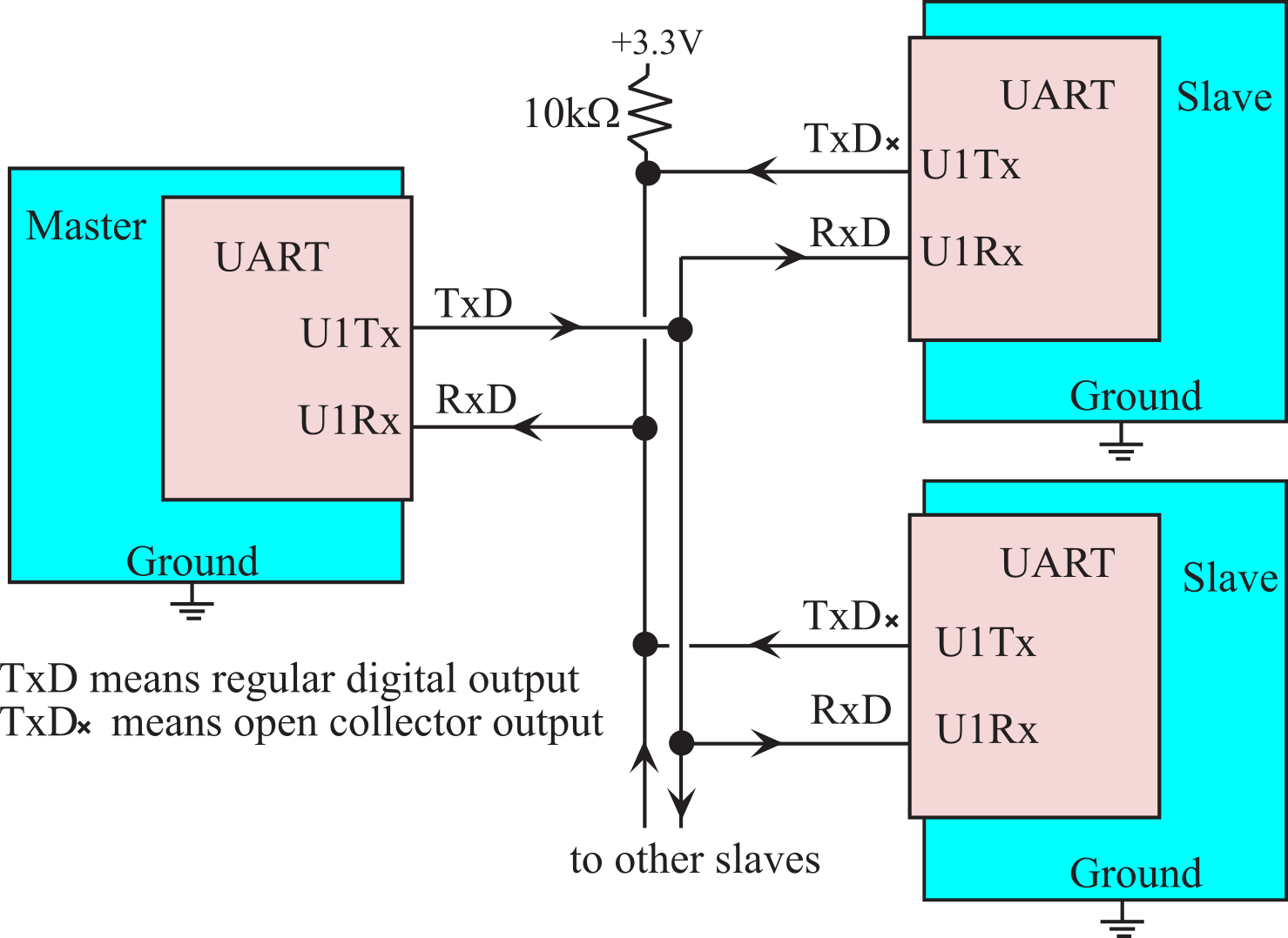
Figure 9.3.1. A master-slave network implemented with multiple microcontrollers.
: What voltage level will the master RxD observe if two slaves simultaneously transmit, one making it a logic high and the other a logic low?
The next communication system is a ring network. This is the simplest distributed system to design, because it can be constructed using standard serial ports. In fact, we can build a ring network simply by chaining the transmit and receive lines together in a circle, as shown in Figure 9.3.2. Building a ring network is a matter as simple as soldering a RS232 cable in a circle with one DB9 connector for each node. Messages will include source address, destination address and information. If computer A wishes to send information to computer C, it sends the message to B. The software in computer B receives the message, notices it is not for itself, and it resends the message to C. The software in computer C receives the message, notices it is for itself, and it keeps the message. Although simple to build, this system has slow performance (response time and bandwidth), and it is difficult to add/subtract nodes.
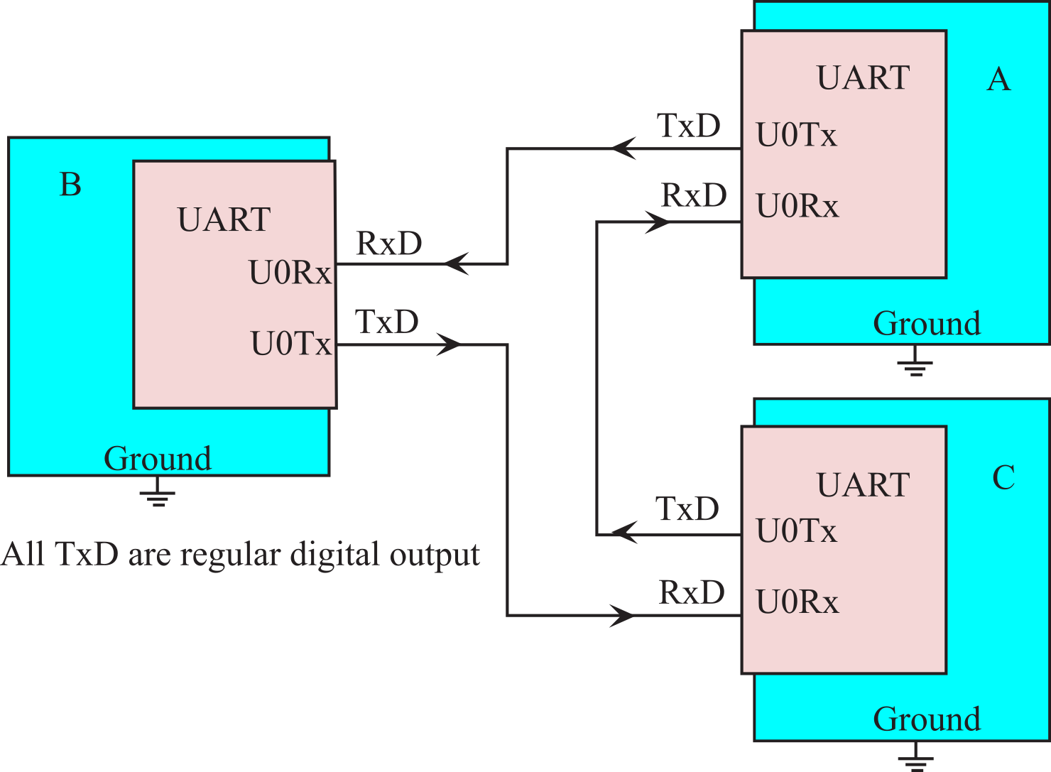
Figure 9.3.2. A ring network implemented with three microcontrollers.
: Assume the ring network has 10 nodes, the baud rate is 100,000 bits/sec, and there are 10 bits/frame. What is average time it takes to send a 10 byte message from one computer to another?
If the distances are short, a multi-drop network can be implemented with simple open collector or open-drain digital-level logic, see Figure 9.3.3. Open drain logic has two output states: low and off. In the off state the output is not driven high or low, it just floats. The 10 kΩ pull-up resistor will passively make the signal high if none of the open drain outputs are low. The microcontroller can make its TxD serial outputs be open drain (ODE on the TM4C). This mode allows a half duplex network to be created without any external logic (although pull-up resistors are often used). Three factors will limit the implementation of this simple half duplex network: 1) the number nodes on the network, 2) the distance between nodes; and 3) presence of corrupting noise. In these situations, a half duplex RS485 driver chip like the SP483 made by Sipex or Maxim can be used. To transmit a byte to the other computers, the software activates the SP483 driver and outputs the frame. Since it is half duplex, the frame is also sent to the receiver of the computer that sent it. This echo can be checked to see if a collision occurred (two devices simultaneously outputting.) If more than two computers exist on the network, we usually send address information first, so that the proper device receives the data. Many collisions can be avoided looking to see if the receiver is active before transmitting.
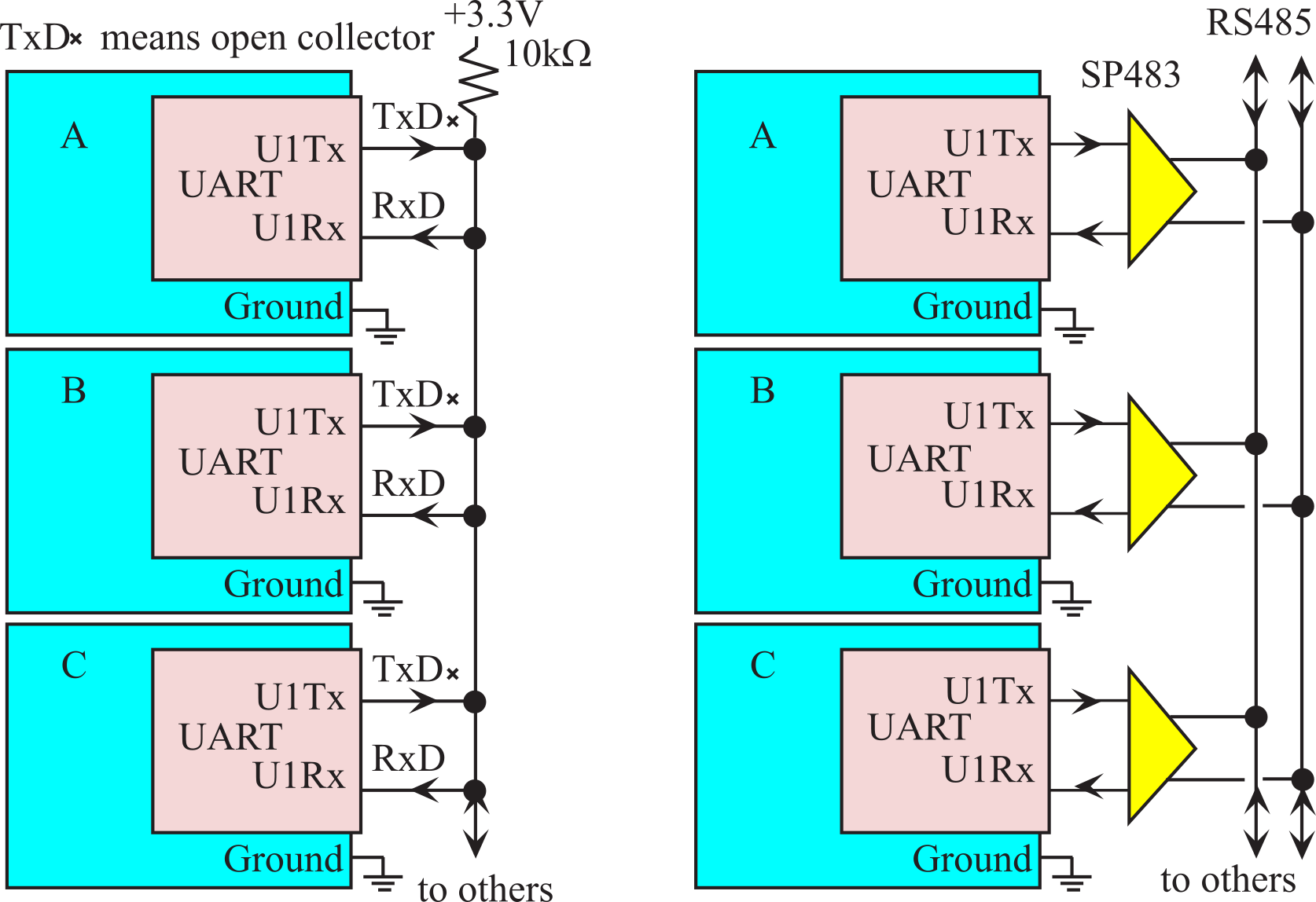
Figure 9.3.3. A multidrop network is created using a half duplex serial channel implemented with open drain logic or with RS485 drivers.
: How can the transmitter detect corrupted data caused by a collision?
: How can the receiver detect corrupted data caused by a collision?
9.4. Bluetooth Low Energy
9.4.1. Fundamentals
Bluetooth is wireless medium and a data protocol that connects devices together over a short distance. Examples of Bluetooth connectivity include headset to phone, speaker to computer, and fitness device to phone/computer. Bluetooth is an important component of billions of products on the market today. Bluetooth operates from 1 to 100 meters, depending on the strength of the radio. Most Bluetooth devices operate up to a maximum of 10 meters. However, in order to improve battery life, many devices reduce the strength of the radio, and therefore save power by operating across distances shorter than 10 meters. If the computer or phone provides a bridge to the internet, a Bluetooth-connected device becomes part of the Internet of Things (IoT).
Bluetooth LE could use any of the 40 narrow bands (LL 0 to 39) at 2.4 GHz; these bands are drawn as bumps in Figure 9.4.1. This figure also shows the WiFi channels, which exist as three wide bands of frequencies, called channel 1, 6 and 11. Because BLE coexists with regular Bluetooth and WiFi, BLE will avoid the frequencies used by other communication devices. LL channels 37, 38 and 39 are used to advertise, and LL channels 9-10, 21-23 and 33-36 are used for BLE communication. BLE has good performance in congested/noisy environments because it can hop from one frequency to another. Frequency Hopping Spread Spectrum (FHSS) rapidly switches the carrier among many frequency channels, using a pseudorandom sequence known to both transmitter and receiver. This way, interference will only affect some but not all communication.
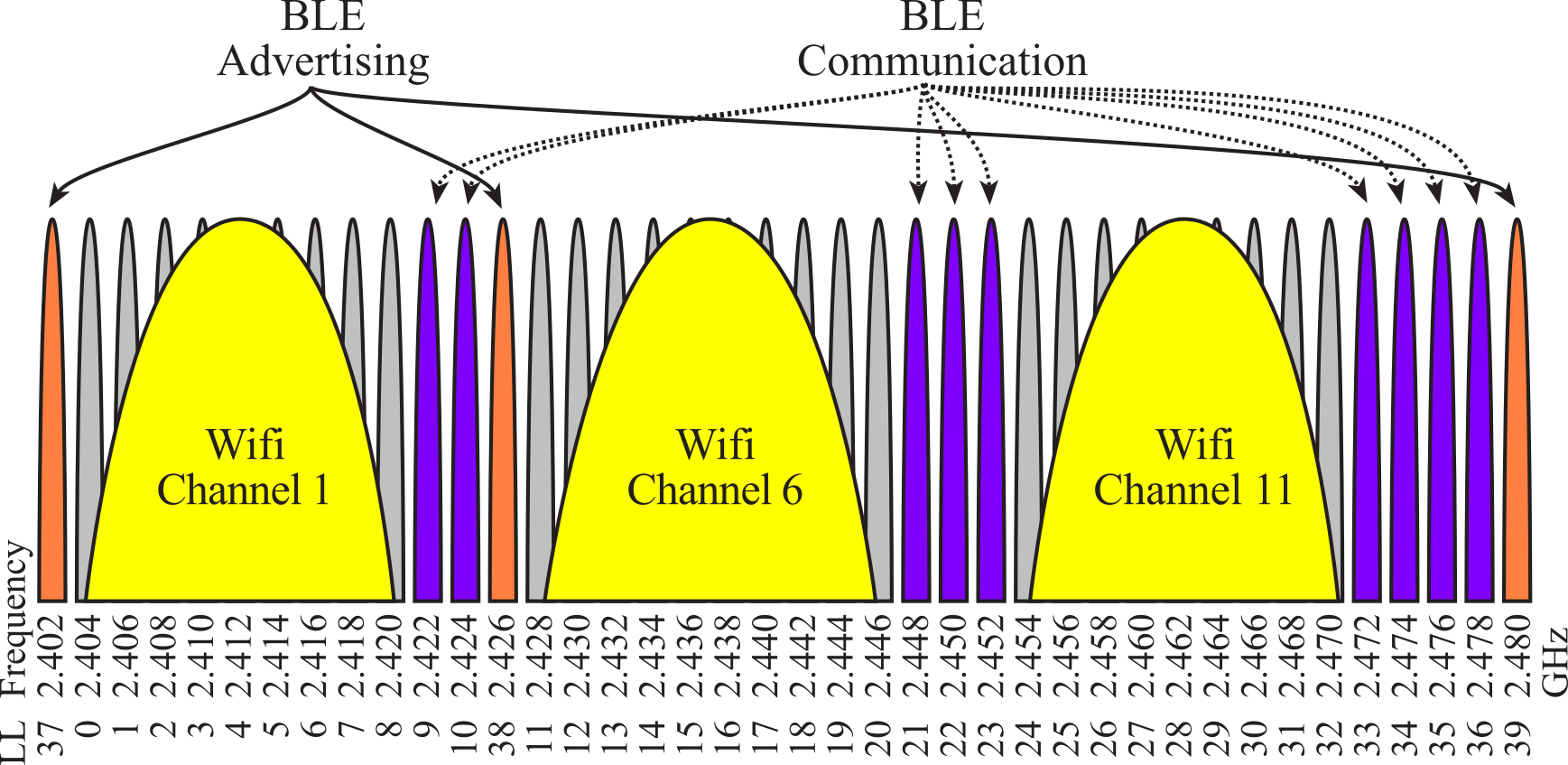
Figure 9.4.1. The 2.4 GHz spectrum is divided into 40 narrow bands, numbered LL 0 to 39. Each band is ±1 MHz.
Figure 9.4.2 illustrated the inverted F shape of the 2.4 GHz antenna used on the CC2650 LaunchPad. For more information on antenna layout, see http://www.ti.com/lit/an/swra351a/swra351a.pdf
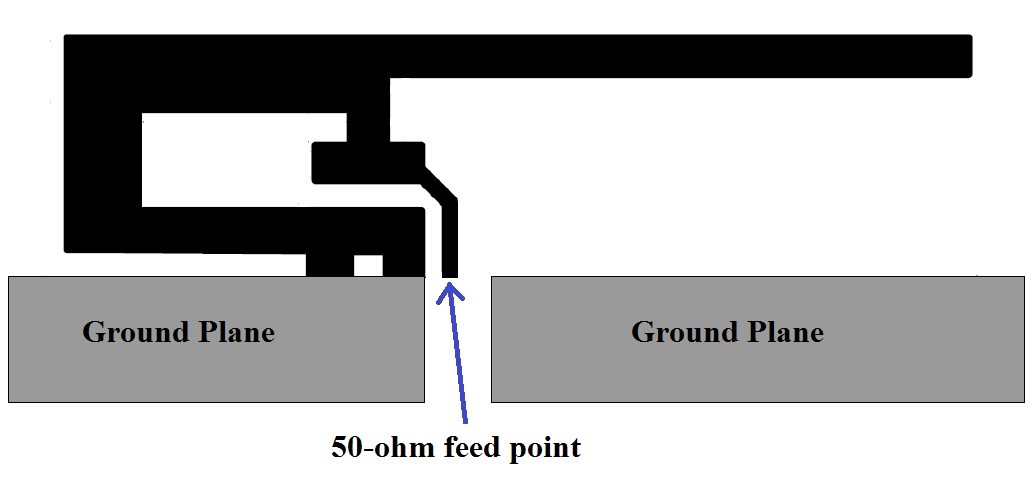
Figure 9.4.2. One possible layout of the 2.4 GHz antenna.
Bluetooth is classified as a personal area network (PAN) because it implements communication within the range of an individual person. Alternatively, devices within a Bluetooth network are usually owned or controlled by one person. When two devices on the network are connected, we often say the devices are paired.
At the highest level, we see Bluetooth devices implement profiles. A profile is a suite of functionalities that support a certain type of communication. For example, the Advanced Audio Distribution Profile (A2DP) can be used to stream data. The Health Device Profile (HDP) is a standard profile for medical devices. There are profiles for remote controls, images, printers, cordless telephones, health devices, hands free devices, and intercoms. The profile we will use in this chapter is the generic attribute protocol (GATT). Within the GATT there can be once or more services. Table 9.4.1 shows some of the services that have been developed.
|
Specification Name |
Assigned Number |
|
Alert Notification Service |
0x1811 |
|
Automation IO |
0x1815 |
|
Battery Service |
0x180F |
|
Blood Pressure |
0x1810 |
|
Body Composition |
0x181B |
|
Bond Management |
0x181E |
|
Continuous Glucose Monitoring |
0x181F |
|
Current Time Service |
0x1805 |
|
Cycling Power |
0x1818 |
|
Cycling Speed and Cadence |
0x1816 |
|
Device Information |
0x180A |
|
Environmental Sensing |
0x181A |
|
Generic Access |
0x1800 |
|
Generic Attribute |
0x1801 |
|
Glucose |
0x1808 |
|
Health Thermometer |
0x1809 |
|
Heart Rate |
0x180D |
|
HTTP Proxy |
0x1823 |
|
Human Interface Device |
0x1812 |
|
Immediate Alert |
0x1802 |
|
Indoor Positioning |
0x1821 |
|
Internet Protocol Support |
0x1820 |
|
Link Loss |
0x1803 |
|
Location and Navigation |
0x1819 |
|
Next DST Change Service |
0x1807 |
|
Object Transfer |
0x1825 |
|
Phone Alert Status Service |
0x180E |
|
Pulse Oximeter |
0x1822 |
|
Reference Time Update Service |
0x1806 |
|
Running Speed and Cadence |
0x1814 |
|
Scan Parameters |
0x1813 |
|
Transport Discovery |
0x1824 |
|
Tx Power |
0x1804 |
|
User Data |
0x181C |
|
Weight Scale |
0x181D |
Table 9.4.1. Adopted GATT services, https://www.bluetooth.com/specifications/gatt/services
Within a service there may be one or more characteristics. A characteristic is user or application data that is transmitted from one device to another across the network. One of the attributes of a characteristic is whether it is readable, writeable, or both. We will use the notify indication to stream data from the embedded object to the smart phone. Characteristics have a universally unique identifier (UUID), which is a 128-bit (16-byte) number that is unique. BLE can use either 16-bit or 32-bit UUIDs. A specific UUID is used within the network to identify a specific characteristic. Often a characteristic has one or more descriptors. Descriptors may be information like its name and its units. We will also see handles, which are a mechanism to identify characteristics within the device. A handle is a pointer to an internal data structure within the GATT that contains all the information about that characteristic. Handles are not passed across the Bluetooth network; rather, handles are used by the host and controller to keep track of characteristics. UUIDs are passed across the network. Figure 9.4.3 shows a GATT service with seven characteristics.
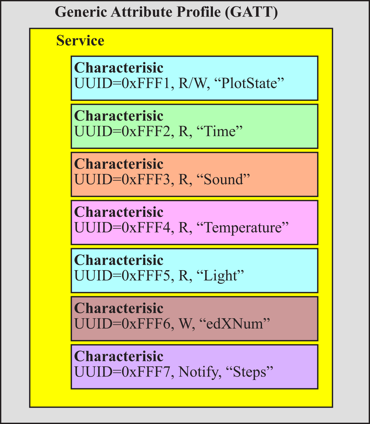
Figure 9.4.3. A GATT profile implements services, and a service has one or more characteristics.
9.4.2. Bluetooth Protocol Stack
The BLE protocol stack includes a controller and a host, as shown in Figure 9.4.4. Bluetooth BR (basic rate), Bluetooth EDR (enhanced data rate), and Bluetooth LE (low energy) all separate the controller and host as different layers and are often implemented separately. The user application and operating system sit on top of the host layer. This section is a brief overview of BLE. For more information on HCI, www.ti.com/ble-wiki and www.ti.com/ble-stack .
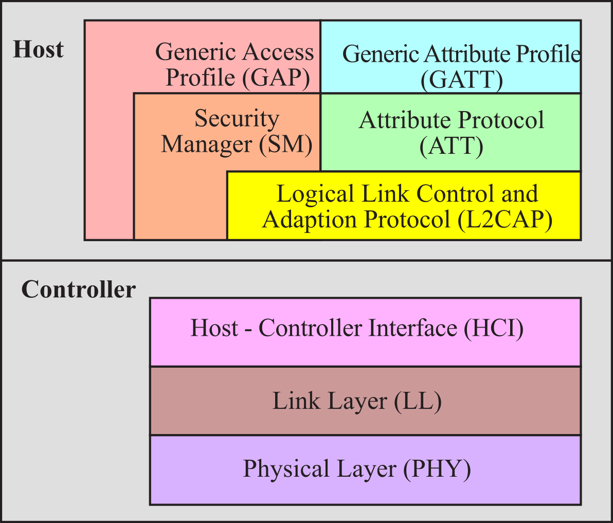
Figure 9.4.4. The BLE stack. These layers are implemented inside the CC2650. The physical layer includes the antenna, which is outside the CC2650.
The physical layer (PHY) is a 1Mbps adaptive frequency-hopping GFSK (Gaussian Frequency-Shift Keying) radio operating in the unlicensed 2.4 GHz ISM (Industrial, Scientific, and Medical) band.
The link layer (LL) controls the radiofrequency state of the device. The device can be in one of five states: standby, advertising, scanning, initiating, or connected. Advertisers transmit data without being in a connection, while scanners listen for advertisers. An Initiator is a device that is responding to an Advertiser with a connection request. If the Advertiser accepts, both the advertiser and initiator will enter a connected state. When a device is in a connection, it will be connected in one of two roles master or slave. The device that initiated the connection becomes the master, and the device that accepted the request becomes the slave. In Lab 6, the embedded system will be an advertiser and the smart phone will be the initiator.
The host control interface (HCI) layer provides a means of communication between the host and controller via a standardized interface. Standard HCI commands and events are specified in the Bluetooth Core Spec. The HCI layer is a thin layer which transports commands and events between the host and controller. The HCI is implemented has function calls and callbacks within the CC2650 controller.
The link logical control and adaption protocol (L2CAP) layer provides data encapsulation services to the upper layers, allowing for logical end-to-end communication of data. The security manager (SM) layer defines the methods for pairing and key distribution, and provides functions for the other layers of the protocol stack to securely connect and exchange data with another device. The generic access protocol (GAP) layer handles the connection and security. In this simple example, we configure the GAP to setup and initiate advertisement. We will use the GAP to connect our embedded system to a smart phone.
The overriding theme of Bluetooth communication is the exchange of data between paired devices. A service is a mechanism to exchange data. A collection of services is a profile. The generic attribute profile (GATT) handles services and profiles. The attribute protocol (ATT) layer protocol allows a device to expose "attributes" to other devices. All data communications that occur between two devices in a BLE connection are handled through the GATT.
The first step for our embedded device to perform is to configure and start advertisement, see Figure 9.4.5. In advertisement mode the device sends out periodic notifications of its existence and its willingness to connect. Another device, such as a smart phone, scans the area for possible devices. If desired this device can request a connection. If the advertiser accepts, both devices enter a connected phase, where the embedded device will be the slave (server) and the initiator becomes the master (client).
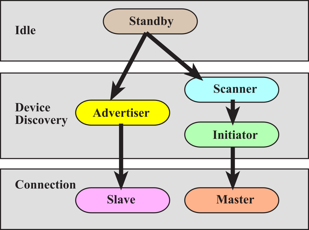
Figure 9.4.5. BLE connection steps.
To save power, the device spends most the time sleeping. The master sends out periodic requests to communicate. If the slave wishes to communicate, the master and slave will exchange data during this connection event. Figure 9.94.6 plots the device current verses time. This graph shows most of the current draw occurs during the connection events. The embedded device can save power by reducing the period of the connection events or by choosing not to participate in all the events.
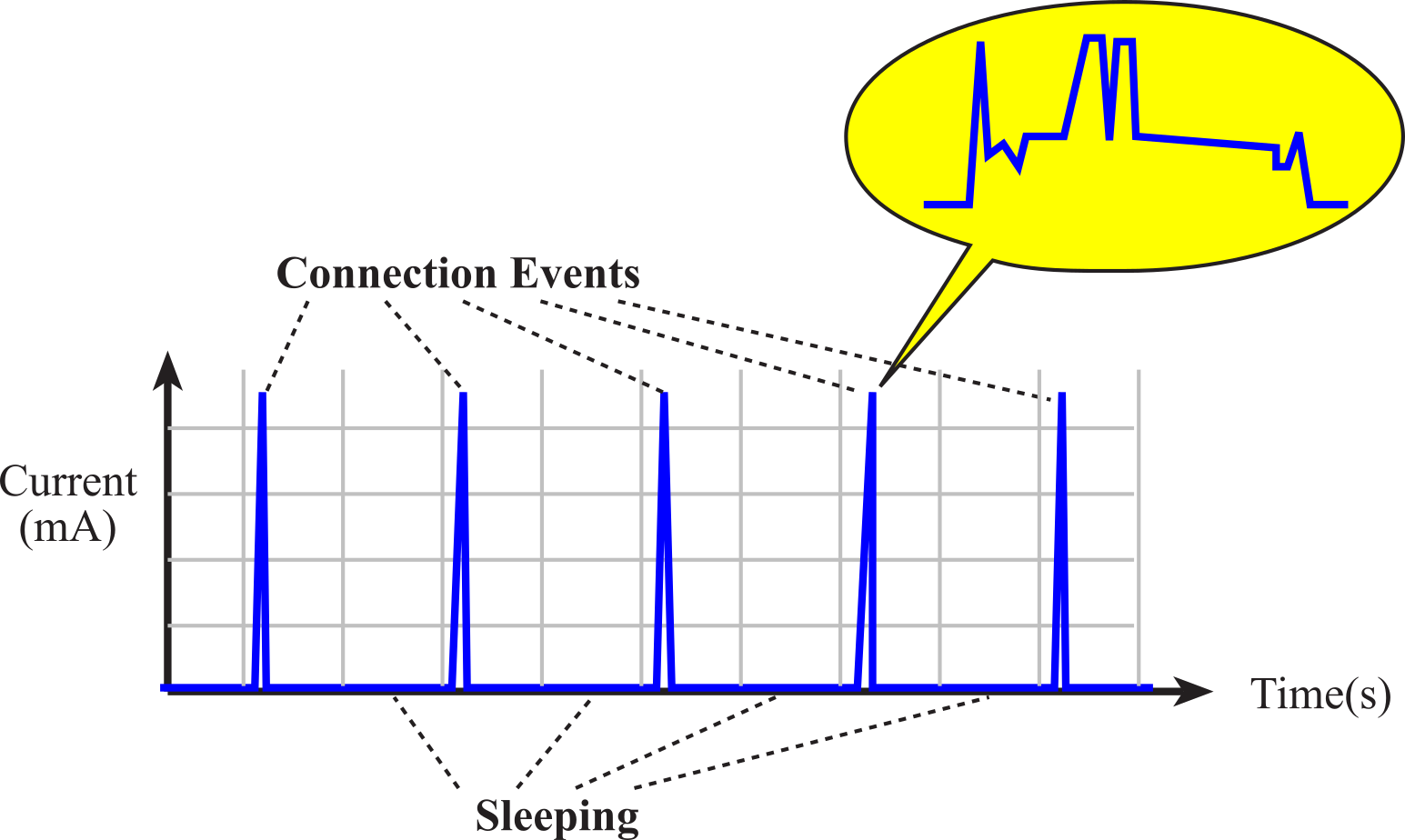
Figure 9.4.6. CC2650 current verses time, showing the connection events.
For example, you will see the advertising interval settings as parameters in the NPI_StartAdvertisement message. In particular, the example projects set the advertising interval to 62.5ms.
9.4.3. Client-server Paradigm
The client-server paradigm is the dominant communication pattern for network protocols, see Figure 9.4.7. In general, the embedded system will be the server, and the smart phone will be the client. The client can request information from the server, or the client can send data to the server. With Bluetooth this exchange of data is managed by the services and profiles, discussed in the next section. There are four main profile types.
A peripheral device has sensors and actuators. On startup it advertises as connectable, and once connected it acts as a slave. In general, the embedded device will be a peripheral.
A central device has intelligence to manage the system. On startup it scans for advertisements and initiates connections. Once connected it acts as the master. In general, the smart phone in will be a central device.
A broadcaster has sensors collecting information that is generally relevant. On startup it advertises but is not connectable. Other devices in the vicinity can read this information even though they cannot connect to the broadcaster. An example is a thermometer.
An observer can scan for advertisements but cannot initiate a connection. An example is a temperature display device that shows temperatures measured by broadcasters.
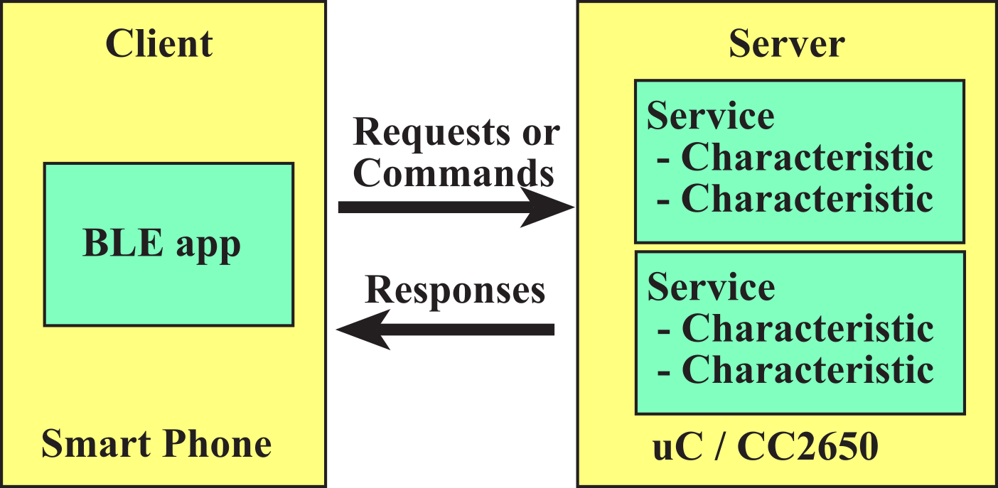
Figure 9.4.7. Client-server Paradigm.
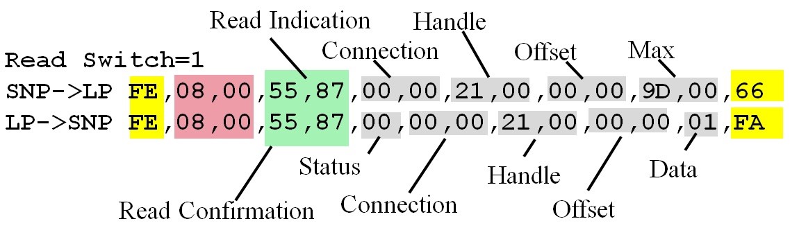
Read indication. When the client wishes to know the value of a characteristic, it will issue a read indication. Inside the request will be a universally unique identifier (UUID) that specifies which characteristic is desired. The server will respond with the value by returning a read confirmation. The data may be one or more bytes. For large amounts of data, the response could be broken into multiple messages. In the example projects, the data will be 1, 2 or 4 bytes long. The size of the data is determined during initialization as the characteristic is configured.
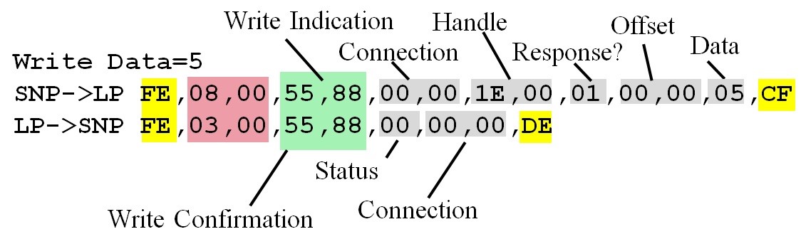
Write indication. When the client wishes to set the value of a characteristic, it will issue a write indication. This request will include data. The request will also include a UUID that specifies to which characteristic the data should be written. The server will respond with an acknowledgement, called a write confirmation.
Notify request. When the client wishes to keep up to data on a certain value in the server, it will issue a notify request. The request includes a UUID. The server will respond with an acknowledgement, and then the server will stream data. This streaming could occur periodically, or it could occur whenever the value changes. In the example projects, notify indication messages are sent from server to client periodically. The client can start notification (listen command on the phone) or stop notifications.
9.4.4. CC2650 Microcontroller
There are three controllers on the CC2650: a main CPU, an RF core, and a sensor controller. Together, these combine to create a one-chip solution for Bluetooth applications. The main CPU includes 128kB of flash, 20kB of SRAM, and a full range of peripherals. Typically, the ARM Cortex-M3 processor handles the application layer and BLE protocol stack. However, in this chapter, we will place the application layer on another processor and use the CC2560 just to implement Bluetooth.
The RF Core contains an ARM Cortex-M0 processor that interfaces the analog RF and base-band circuitries, handles data to and from the system side, and assembles the information bits in a given packet structure. The RF core offers a high level, command-based API to the main CPU. The RF core is capable of autonomously handling the time-critical aspects of the radio protocols (802.15.4 RF4CE and ZigBee, Bluetooth Low Energy) thus offloading the main CPU and leaving more resources for the user application. The RF core has its own RAM and ROM. The ARM Cortex-M0 ROM is not programmable by customers. The basic circuit implementing the 2.4 GHz antenna is shown in Figure 9.4.8.
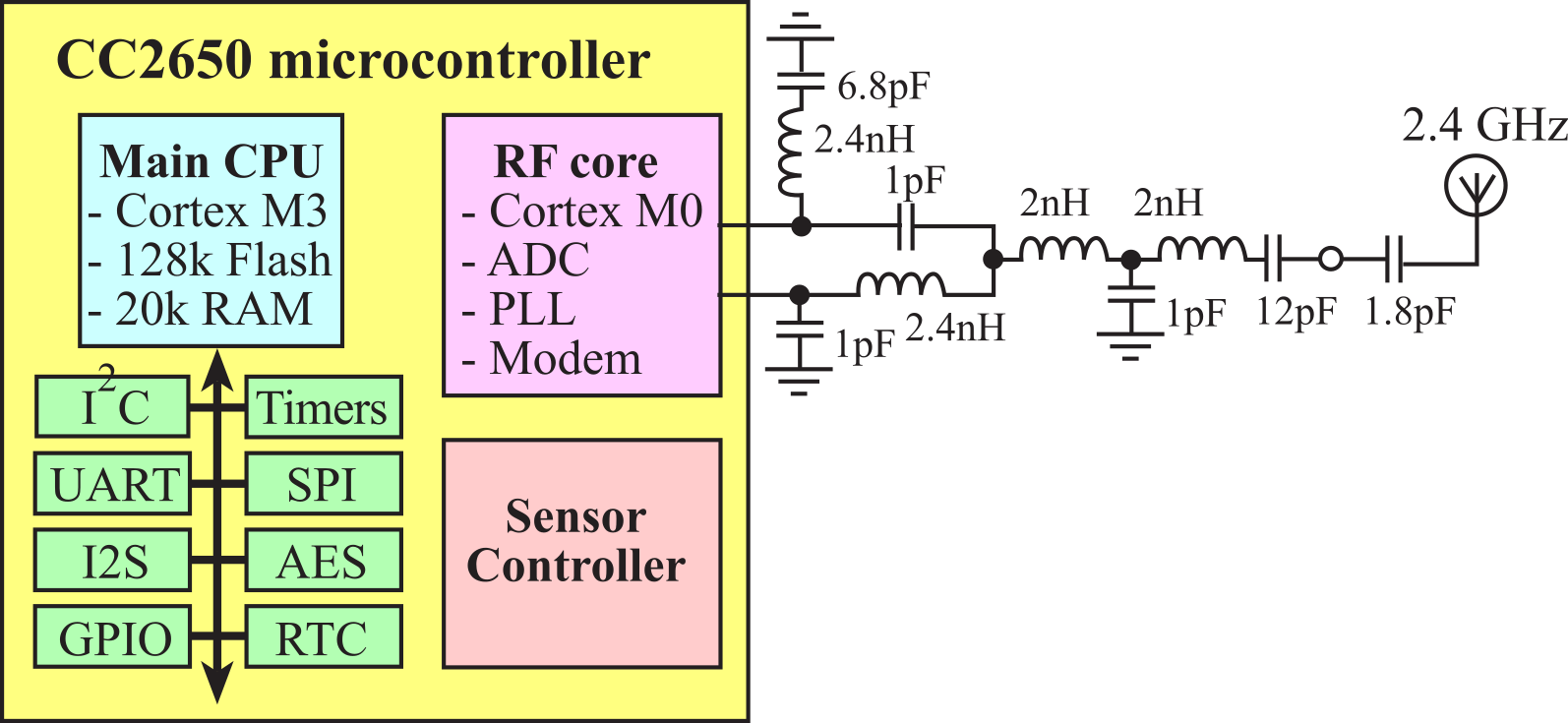
Figure 9.4.8. The CC2650 includes a main CPU, a suite of I/O devices, an RF core, and a sensor controller.
The Sensor Controller block provides additional flexibility by allowing autonomous data acquisition and control independent of the main CPU, further extending the low-power capabilities of the CC2650. The Sensor Controller is set up using a PC-based configuration tool, called Sensor Controller Studio, and example interfaces include:
• Analog sensors using integrated ADC
• Digital sensors using GPIOs, bit-banged
I2C, and SPI
• UART communication for sensor reading
or debugging
• Capacitive sensing
• Waveform generation
• Pulse counting
• Keyboard scan
• Quadrature decoder for polling rotation
sensors
• Oscillator calibration
The CC2650 uses a radio-frequency (RF) link to implement Bluetooth Low Energy (BLE). As illustrated in Figure 9.4.9, the CC2650 can be used as a bridge between any microcontroller and Bluetooth. It is a transceiver, meaning data can flow across the link in both directions.
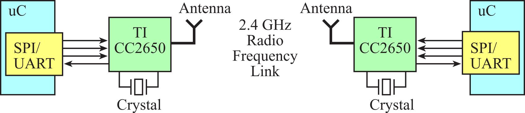
Figure 9.4.9. Block diagram of a wireless link between two microcontroller systems.
Figure 9.34 shows a CC2650 BoosterPack. This board comes preprogrammed with the simple network processor described in the next section. With a JTAG debugger, other programs can be loaded onto this CC2650. For more information, see
http://www.ti.com/tool/boostxl-cc2650ma
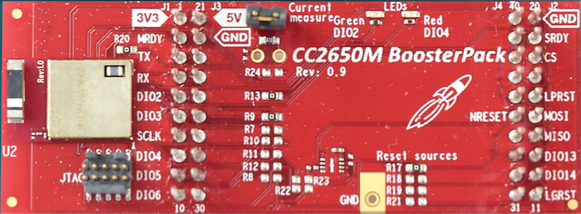
Figure 9.4.10. CC2650 BoosterPack (BOOSTXL-CC2650MA).
Figure 9.4.11 shows a CC2650 LaunchPad. The top part of the PCB is the debugger and the bottom part implements the CC2650 target system. To see the pin connections, see
http://www.ti.com/ww/en/launchpad/launchpads-connected-launchxl-cc2650.html
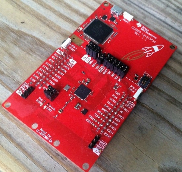
Figure 9.4.11. CC2650 LaunchPad (LAUNCHXL-CC2650).
9.4.5. Single Chip Solution, CC2650 LaunchPad
The CC2650 microcontroller is a complete System-on-Chip (SoC) Bluetooth solution, as shown in Figure 9.4.12. One could deploy the application, the Bluetooth stack, and the RF radio onto the CC2650.
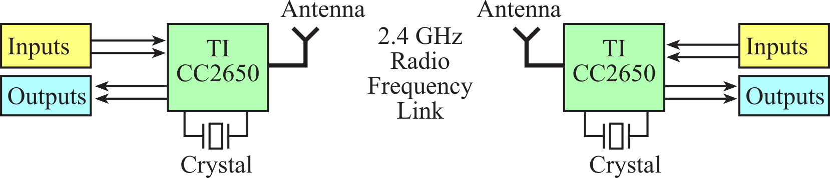
Figure 9.4.12. Block diagram of a wireless link between two single-chip embedded systems.
9.4.6. Network Processor Interface (NPI)
Simple Network Processor (SNP) is TI's name for the application that runs on the CC2650 when using the CC2650 with another microcontroller such as the MSP432 or TM4C123. In this configuration the controller and host are implemented together on the CC2650, while the profiles and application are implemented on an external MCU. The application and profiles communicate with the CC2650 via the Application Programming Interface (API) that simplifies the management of the BLE network processor. The SNP API communicates with the BLE device using the Network Protocol Interface (NPI) over a serial (SPI or UART) connection. In this chapter, we will use a UART interface as shown in Figure 9.37. This configuration is useful for applications that wish to add Bluetooth functionality to an existing device. In this paradigm, the application runs on the existing microcontroller, and BLE runs on the CC2650. For a description of the Simple Network Processor, refer to
SNP http://processors.wiki.ti.com/index.php/CC2640_BLE_Network_Processor
Developer guide http://www.ti.com/lit/ug/swru393c/swru393c.pdf
TI wiki page http://processors.wiki.ti.com/index.php/NPI
In this section, our TM4C123/MSPM0 LaunchPad will be the application processor (AP) and the CC2650 will be the network processor (NP). There are 7 wires between the AP and the NP. Two wires are power and ground, one wire is a negative logic reset, two wires are handshake lines, and two wires are UART transmit and receive.
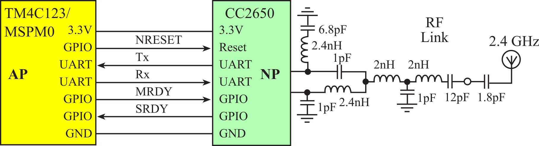
Figure 9.4.13. Hardware interface between the LaunchPad AP and the CC2650 NP.
To initialize Bluetooth, the master (AP) first resets the slave (NP). The reset line is a GPIO output of the AP and is the hardware reset line on the NP. There are two handshake lines: master ready and slave ready. Master ready (MRDY) is a GPIO output of the AP and a GPIO input to the NP. Slave ready (SRDY) is a GPIO output of the NP and a GPIO input of the AP. If the AP wishes to reset the NP, it sets MRDY high and pulses reset low for 10 ms, Figure 9.4.14. Normally, the reset operation occurs once, and thereafter the reset line should remain high.
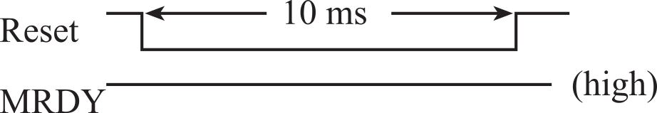
Figure 9.4.14. The LaunchPad AP can reset the CC2650 NP.
There are two types of communication. Messages can be sent from master to slave, or from slave to master. If the master (AP) wishes to send a message to the slave (NP), it follows 5 steps, Figure 9.4.15. First, the master sets MRDY low (Master: "I wish to send"). Second, the slave responds with SRDY low (Slave: "ok, I am ready"). The communication is handshaked because the master will wait for SRDY to go low. Third, the master will transmit a message on its UART output (Rx input to slave). The format of this message will be described later. Fourth, after the message has been sent, the master pulls MRDY high (Master: "I am done"). Fifth, the slave pulls its SRDY high (Slave: "ok"). Again, the handshaking requires the master to wait for SRDY to go high.
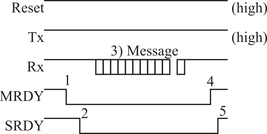
Figure 9.4.15. The LaunchPad AP can send a message to the CC2650 NP. Handshake means the steps 1 - 5 always occur in this sequence.
If the slave (NP) wishes to send a message to the master (AP), there are also 5 steps, Figure 9.4.16. First, the slave sets SRDY low (Slave: "I wish to send"). Second, the master responds with MRDY low (Master: "ok, I am ready"). You will notice in the example projects that the master will periodically check to see if the SRDY line has gone low, and if so it will receive a message. Third, the slave will transmit a message on its UART output (Tx output from slave). The format of this message will be the same for all messages. Fourth, after the message has been sent, the slave pulls SRDY high (Slave: "I am done"). The master will wait for SRDY to go high. Fifth, the master pulls its MRDY high (Master: "ok").
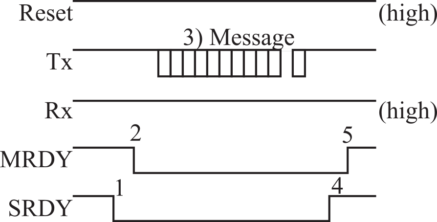
Figure 9.4.16. The CC2650 NP can send a message to the LaunchPad AP. Handshake means the steps 1 - 5 always occur in this sequence.
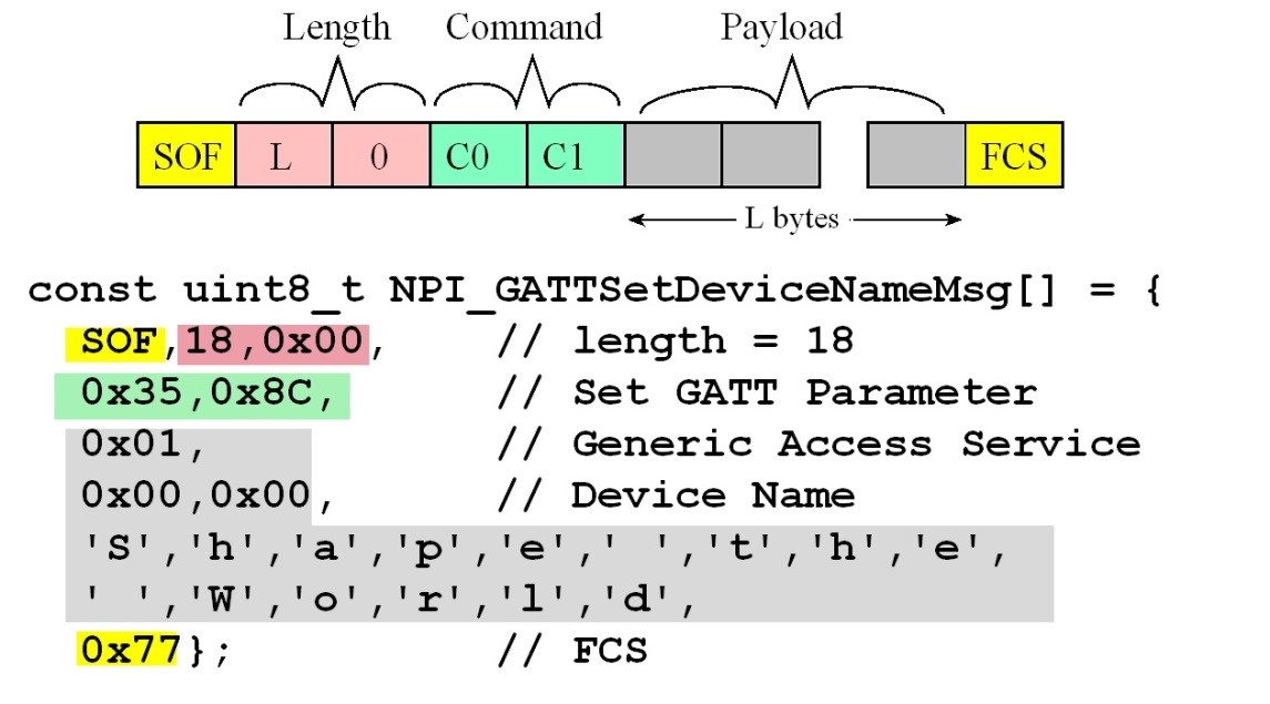
The format of the message is shown in Figure 9.4.17. The boxes in the figure represent UART frames. Each UART frame contains 1 start bit, 8 data bits, and 1 stop bit, sent at 115,200 bits/sec. All messages begin with a start of frame (SOF), which is a 254 (0xFE). The next two bytes are the payload length in little endian format. Since all the payloads in this chapter are less than 256 bytes, the second byte is the length, L, and the third byte is 0. The fourth and fifth bytes are the command. Most commands have a payload, which contains the parameters of the command. Some commands do not have a payload. All messages end with a frame check sequence (FCS). The FCS is the 8-bit exclusive or of all the data, not including the SOF and the FCS itself.
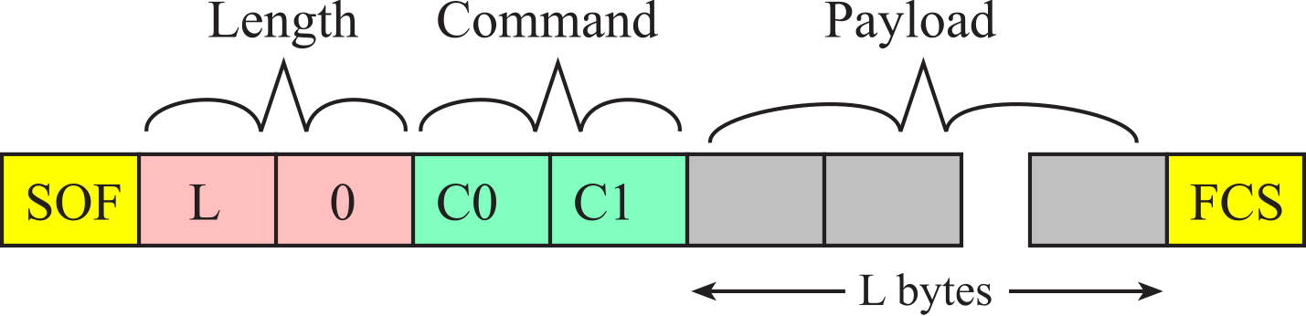
Figure 9.4.17. The format of an NPI message.
The following steps occur in this order
1. Initialize GATT (add services,
characteristics, CCCD's); After the CC2650 is reset, the next step is to services
and characteristics. In the example projects we will define one service with
multiple characteristics. To create a service, the master first issues an Add
Service command (0x35,0x81). For each characteristic, the master sends an Add
Characteristic Value (0x35,0x82) and an Add Characteristic Description
(0x35,0x83) message. Once all the characteristics are defined, the master sends
a Register Service command (0x35,0x84). Each of the commands has an
acknowledgement response. The debugger output for a service with one
characteristic is shown in Figure 9.4.18. The detailed syntax of these messages
can be found in the TI CC2640 Bluetooth low energy Simple Network Processor API
Guide.
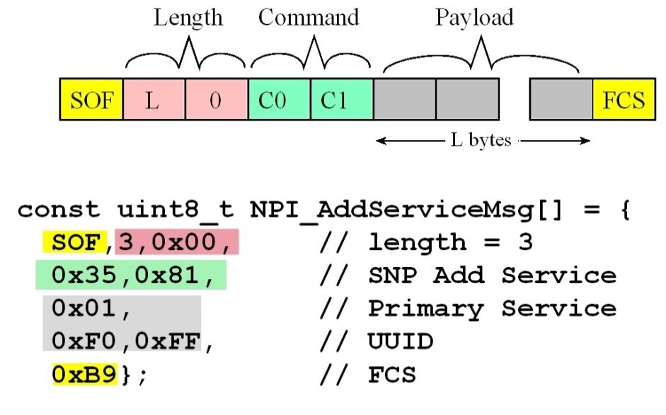
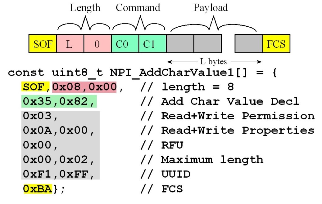
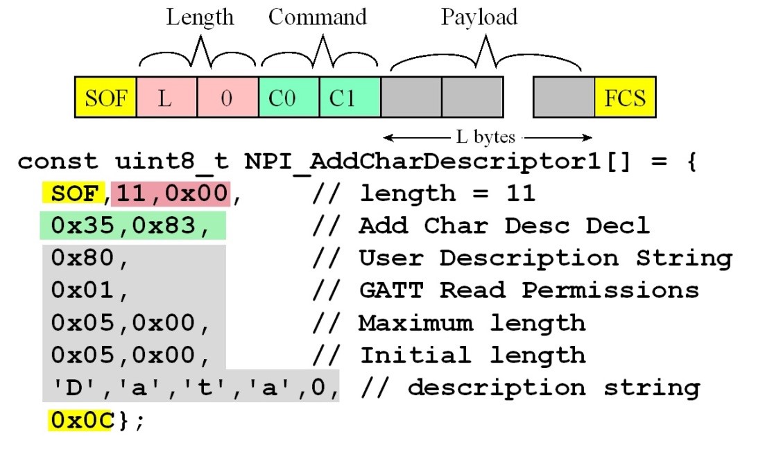
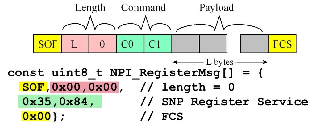
Add service Figure 9.4.18. TExaSdisplay output as the device sets up a
service with one characteristic. These data were collected running the
VerySimpleApplicationProcessor project. Figures 9.4.19 through 9.4.22 show the four messages used
to define a service with one characteristic. The add service creates a
service. The add characteristic value declaration defines the
read/write/notify properties of a characteristic in that service. The response
to this message includes the handle. The add characteristic description
declaration defines the name of the characteristic. When we create services
with multiple characteristics, we simply repeat the "add characteristic value"
and "add characteristic description" declarations for each. The register service
makes that service active. Figure 9.4.19. Add service message from the
VerySimpleApplicationProcessor project. Figure 9.4.20. Add characteristic value declaration message
from the VerySimpleApplicationProcessor project. Figure 9.4.21. Add characteristic declaration message from
the VerySimpleApplicationProcessor project. Figure 9.4.22. Register service message from the
VerySimpleApplicationProcessor project. After all the services and characteristics are defined,
the master will setup and initiate advertising. The master will send four
messages to set up advertising. The debugger output for advertising is shown in
Figure 9.4.23. Each message will be acknowledged by the NP. A 0x35,0x85 message
will set the device name. There are two 0x55,0x43 messages to configure the
parameters of the advertising. The 0x55,0x42 message will start advertising.
Again, detailed syntax of these messages can be found in the TI CC2640
Bluetooth low energy Simple Network Processor API Guide. Figure 9.48 shows the
C code to define a Set Device Name message.
GATT Set DeviceName Figure 9.4.23. TExaSdisplay output as the device sets up
advertising. These data were collected running the
VerySimpleApplicationProcessor project. Figure 9.4.24. A set device name message from the VerySimpleApplicationProcessor
project. Figure 9.4.25 shows the message exchange when the client
issues a read request. The NP sends a read indication to the AP,
containing the connection and handle of the characteristic. The
AP responds with a read confirmation containing status, connection, handle, and
the data. Figure 9.4.25. TExaSdisplay output occurring when the
client issues a read request. These data were collected running the
VerySimpleApplicationProcessor project. Figure 9.4.26 shows the message exchange when the client
issues a write request. The NP sends a write indication to the AP,
containing the connection, handle of the characteristic, and the data to be
written. The AP responds with a write confirmation containing status,
connection, and handle. Figure 9.4.26. TExaSdisplay output occurring when the
client issues a write request. These data were collected running the
VerySimpleApplicationProcessor project. One simple low bandwidth and low power protocol is subGHz,
which is part of the IEEE 802.15.4 standard.
This class of communication is called WPAN, wireless
personal area network. The TI CC1352R and Seeed HC12 support subGHz. There
is no addressing, security or error detection/correction. The software can
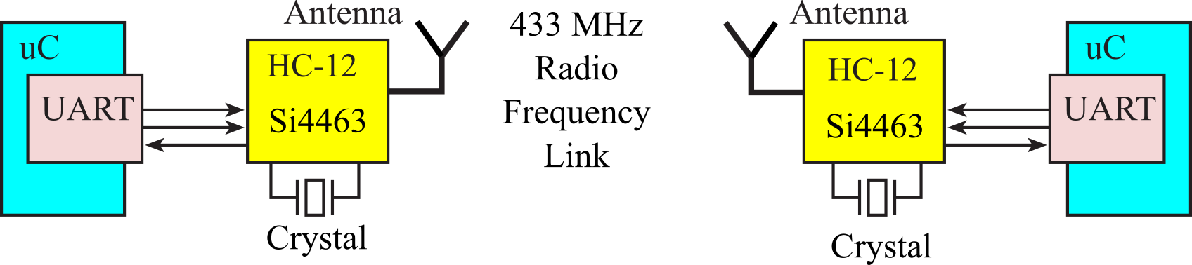
adjust electrical power to improve bandwidth and/or distance. As illustrated in Figure 9.5.1, the Seeed HC-12 implements
a simple subGHz wireless protocol. The HC12 includes a STM8S003F3
microcontroller and the Si4463 with subGHz protocol in firmware. Basically, the
microcontroller on the left transmits data via its UART, and the microcontroller
on the right receives the data with its UART. With a baud rate of 9600, this
interface can transmit 960 bytes/sec. It is a transceiver, meaning data can
flow across the link in both directions. Figure 9.5.1. Block diagram of a
wireless link between two microcontroller systems. Figure 9.5.2 shows the subGHz antenna. Even though the
physical length is about 2.4 cm, the effective length (stretched out) is about
17 cm. Figure 9.5.2. The subGHz antenna is 2.4 cm long, but has a
stretched-out length of 17 cm. The speed of light in air is about ν = 2.997*1010
cm/sec. We can estimate the wavelength of the 433 MHz signal ν = f λ Therefore, the wavelength is 69.2 cm (2.997*1010
cm/sec/433MHz). ¼λ is 17.3 cm, matching the effective length of the
antenna. ZigBee is another low-cost wireless solution for
embedded systems. The name is derived from the behavior of honeybees. Honeybees
distributed across a large open field implement a mesh network to communicate
information to their hive. They do this by message relaying. A bee distant from
the hive will fly a particular zigzag pattern that represents the information.
A second bee nearer the hive will repeat the pattern. The relay continues until
the information reaches the hive. ZigBee is a standard that defines a set of
communication protocols for low-data-rate, very low-power, short-range wireless
networking. It can operate under battery power, and last for years because
there are multiple types of low-power sleep modes. It is an appropriate
solution for sensor networks, meter reading, industrial automation, security
systems, and patient monitoring. ZigBee is an extension of the IEEE 802.15.4b
standard. It is lower cost and lower performance than Bluetooth or IEEE
801.11b, as shown in Table 9.6.1. The range values in this table represent
performance indoors-outdoors. ZigBee modules come in a variety of power versus
performance models. In other words, you can run at lower power if you are
willing to sacrifice distance and data rate. Data
rate Range Wireless
applications ZigBee/subGHz 20
to 250 Kbps 10-100m Sensor
Networks Bluetooth 1
to 3 Mbps 2-10m Headset,
mouse IEEE
802.11b 1
to 11 Mbps 38-140m Internet
connection IEEE
802.11g 1
to 54 Mbps 38-140m Internet
connection IEEE
802.11n 1
to 72 Mbps 70-250m Internet
connection Table 9.6.1. Comparison of wireless protocols. The ZigBee protocol is layered. The top layer is the
application layer, implemented as the user program. At this layer software in
one node sends messages to another node. This section will focus on this layer,
because we will purchase a ZigBee module that performs the lower layers
automatically. The second layer is the application support sublayer (APS).
Below the APS is the network layer (NWK). Below the NWK is the media access
control (MAC) layer. Below the MAC is the physical layer, which includes the RF
transmitter and receiver. ZigBee is a personal area network (PAN),
as shown in Figure 9.6.1. There can be a coordinator, devices that support all
functions, or devices that support some functions. A typical application of
ZigBee is a remote sensor network. Each node in Figure 9.6.1 is capable of
collecting sensor data. The sensor database can be centralized at the PAN
coordinator or distributed across the entire system. Figure 9.6.1. ZigBee used to create a remote sensor network. One low-cost implementation of
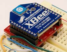
ZigBee is the XBee module from Digi (formally MaxStream), see Figure 9.6.2.
These modules take ZigBee and wrap it into a simple-to-use serial command set,
called AT commands. These modules allow a very reliable and simple
communication between microcontrollers with a serial port. Both point-to-point
and multi-point networks are supported. Figure 9.6.2. The XBee module implements ZigBee https://www.digi.com/products/embedded-systems/digi-xbee/rf-modules
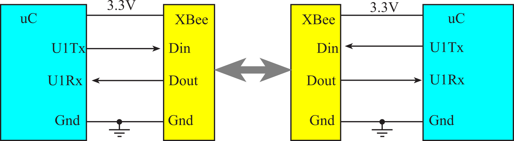
. The hardware involves interfacing 3.3 V full duplex serial
channel to the XBee module, as shown in Figure 9.6.3. Figure 9.6.3. Circuit diagram for a 2-node ZigBee network.
Power and grounds are shared between the microcontroller and its XBee but not
between XBees. In this simple configuration, there can be up to 256 nodes
on the network. The initialization software must establish the baud rate at
9600 bits/sec. The system bandwidth therefore will be on the order of 960
bytes/sec. The <CR> symbol refers to the carriage return, character 13,
existing as one 8-bit ASCII character. To place the XBee in AT command mode, we
execute steps 1 to 5 over and over until we get an OK response. 1.
Send a dummy character like 'X'. 2.
Wait 1.1 second (greater than the one second guard time). 3.
Output "+++". 4.
Wait 1.1 second (greater than the one second guard time). 5.
Wait for response, should be OK<CR>. Each node must establish its address (called my) and the
destination address. For example, if this computer is at address 0x01 and
wishes to send packets to the computer at address 0x02, then this computer
executes these AT commands. The software should wait 20 ms after each AT
command. When an AT command is executed correctly, the XBee responds with OK<CR>.
One of the simplest modes is Application Programming Interface (API)
mode 1, which allows the nodes to send and receive packets: ATDL02<CR>
Sets destination address to 2 (number given in hexadecimal) ATDH0<CR> Sets
destination high address to 0 ATMY01<CR>
Sets my address to 1 (number given in hexadecimal) ATAP1<CR>
Sets API mode 1 (packets) ATCN<CR>
Ends command mode The other node in the point-to-point connection performs a
similar initialization, but obviously with the my and destination
addresses reversed. Using the API mode simplifies the application software,
because all message routing, error detection/retransmission, and message
acknowledgement occurs at lower levels automatically. A data transmission frame
has the following format: 0x7E,
LengthHi, LengthLo, 0x01, ID, DestHi, DestLo, 0x00, b1, ..., bn, Chksum All API mode 1 frames begin with 0x7E. The next two bytes
are the length of the message, which will be the number of bytes after the
length and before the checksum. The length does not include the four bytes
comprising the 0x7E, which is the length itself and the checksum. The fourth
byte 0x01 signifies this is a transmit data packet. The ID should be used as a
message sequence number. I.e., as this computer sends packets to the
destination computer, the ID is sequenced as 1, 2, ... 255, 1, 2, ... An ID
of 0 is not used. This sequence number guarantees the packets arrive at the
destination in the same order as they were sent. The two bytes DestHi,DestLo
specify the destination node address. The high byte should be zero for this
configuration. The next byte provides options for the frame, which should be 0.
Bytes b1 through bn are the data to be transmitted. Because there
is a frame length, this data can be formatted however you wish. The last byte
of the frame will be a checksum. Let sum be the 8-bit addition of all
bytes not including 0x7E delimiter and the length. We calculate Chksum as 0xFF-sum. In this way the
receiver can add up all the bytes after the length and include the Chksum
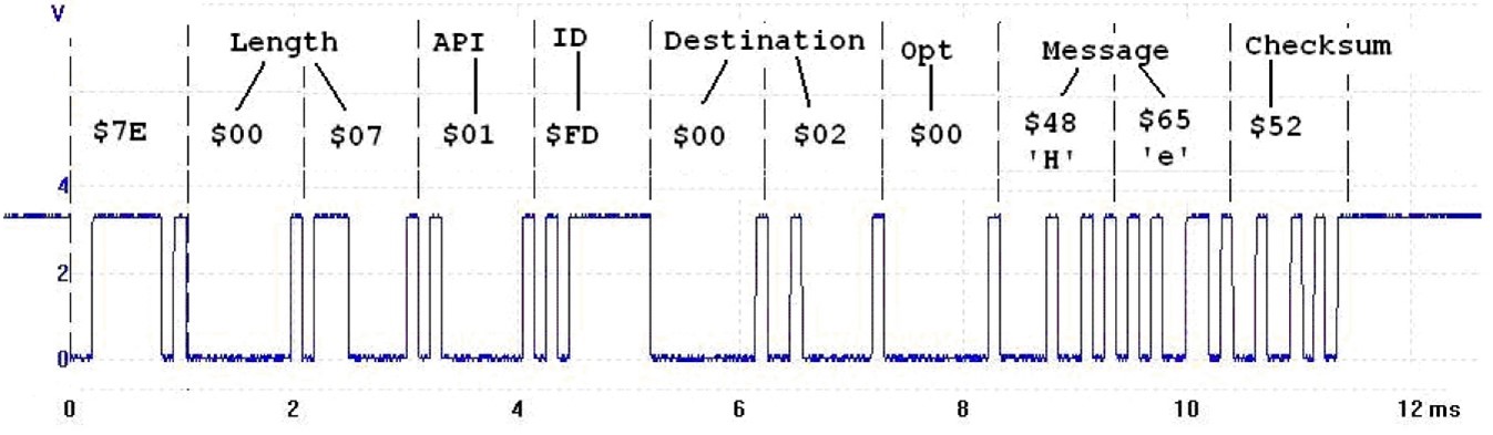
in order to get the result 0xFF. For example, assume we wish to send the message "He" to
node 2. Also assume this is the 254th frame sent, so the ID will be 0xFD.
The message has a length of 7. The checksum is calculated as 0xFF‑(0x01+0xFD+0x00+0x02+0x00+0x48+0x65) = 0x52. The oscilloscope recording for this frame is shown in
Figure 9.6.4. Figure 9.6.4. API transmit frame measured on the Din pin
of the XBee module. When the transmitted frame is properly delivered, the XBee
sends an acknowledgment to the transmitter. The length is always 3 bytes. The
API code is 0x89. The ID matches the corresponding value of the
transmitted frame. The next byte is a status field, and 0x00 means success. A
status of 0x01 means no acknowledgement received, which may mean the
destination node does not exist or is turned off. A status of 0x02 means CCA
failure and 0x03 means the message was purged. The Chksum byte is
calculated in the same manner as all the API frames. 0x7E,
0x00, 0x03, 0x89, ID, 0x00, Chksum The ID of this frame is 0xC1. The checksum for this frame is 0xFF-(0x89+0xC1+0x00) = 0xB5. The receiver with a my
address matching the destination address of the transmitted frame will
be given that frame as an API packet type 0x81. A data receive frame has the
following format: 0x7E,
LengthHi, LengthLo, 0x81, SourceHi, SourceLo, RSSI, 0x00, b1, ..., bn, Chksum The source field identifies the node that sent the
message. The RSSI (received signal strength indictor) is the decimal
equivalent measure of the signal. For example, 0x3A means the received signal
strength is 58 dBm. The option field should be zero. Bytes b1 through bn
contain data. Lab 9 for this course can be downloaded from this link
Lab09.docx
Each lab also has a report
Lab09Report.docx and
Reprinted with approval from
Embedded Systems: Real-Time Interfacing to ARM Cortex-M Microcontrollers, ISBN-13: 978-1463590154
2. Initialize GAP (advertisement data,
connection parameters);
3. Advertise and optionally wait for a
connection;
4. Respond to GATT requests and send
notifications / indications as desired.
LP->SNP FE,03,00,35,81,01,F0,FF,B9
SNP->LP FE,01,00,75,81,00,F5
Add CharValue1
LP->SNP FE,08,00,35,82,03,0A,00,00,00,02,F1,FF,BA
SNP->LP FE,03,00,75,82,00,1E,00,EA
Add CharDescriptor1
LP->SNP FE,0B,00,35,83,80,01,05,00,05,00,44,61,74,61,00,0C
SNP->LP FE,04,00,75,83,00,80,1F,00,6D
Register service
LP->SNP FE,00,00,35,84,B1
SNP->LP FE,05,00,75,84,00,1C,00,29,00,C1
LP->SNP FE,12,00,35,8C,01,00,00,53,68,61,70,65,20,74,68,65,20,57,6F,72,6C,64,DE
SNP->LP FE,01,00,75,8C,00,F8
SetAdvertisement1
LP->SNP FE,0B,00,55,43,01,02,01,06,06,FF,0D,00,03,00,00,EE
SNP->LP FE,01,00,55,43,00,17
SetAdvertisement2
LP->SNP FE,1B,00,55,43,00,10,09,53,68,61,70,65,20,74,68,65,20,57,6F,...,00,0C
SNP->LP FE,01,00,55,43,00,17
StartAdvertisement
LP->SNP FE,0E,00,55,42,00,00,00,64,00,00,00,00,01,00,00,00,C5,02,BB
SNP->LP FE,03,00,55,05,08,00,00,5B
9.5. SubGHz Wireless
9.6. ZigBee
9.7. Lab 9 Audio Communication
This work is based on the course ECE445L
taught at the University of Texas at Austin. This course was developed by Jonathan Valvano, Mark McDermott, and Bill Bard.
Embedded Systems: Real-Time Interfacing to ARM Cortex-M Microcontrollers by Jonathan Valvano is
licensed under a Creative
Commons
Attribution-NonCommercial-NoDerivatives 4.0 International License.