Chapter 3. Human Interfaces
Table of Contents:
- 3.1. Serial Interfaces
- 3.1.1. Timing Diagrams
- 3.1.2. Universal Asynchronous Receiver Transmitter (UART)
- 3.1.3. Serial Peripheral Interface (SPI)
- 3.1.4. Inter-integrated Circuit (I2C)
- 3.1.5. Universal Serial Bus (USB)
- 3.2. Edge Triggered Interrupts
- 3.3. Touch Screens
- 3.4. Keyboards
- 3.5. Displays
- 3.6. Buzzer
- 3.7. Scheming and Teaming
- 3.7.1. Design steps
- 3.7.2. Modular Programming
- 3.7.3. Clients and Coworkers
- 3.7.4. Software Performance Metrics
- 3.7.5. Enhancing Team Skills
- 3.8. Software Style Guidelines
- 3.8.1. Variables
- 3.8.2. Organization of a code file
- 3.8.3. Organization of a header file
- 3.8.4. Formatting
- 3.8.5. Code Structure
- 3.8.6. Naming convention
- 3.8.7. Comments
- 3.9. Lab 3
The theme of this chapter is human interfaces, which are
devices that allow human input to the system, or provide output to the human user.
Switches and LEDs were presented in Section 1.8. However, we will
extend the switch interface to deploy edge-triggered interrupts. Many
input/output devices are highly integrated, and the interface to the device
uses a serial standard like UART, SPI, I2C, and USB. So, we begin this chapter
with four possible serial interfaces.
3.1. Serial Interfaces
3.1.1. Timing Diagrams
When connecting a digital output to a digital input, it is important to manage when events occur. Typical events include the rise or fall of control signals, when data pins need to be correct, and when data pins contain the proper values. In this book, we will use two mechanisms to describe the timing of events. First, we present a formal syntax called timing equations, which are algebraic mechanisms to describe time. Then, we will present graphical mechanisms called timing diagrams.
When using a timing equation, we need to define a zero-time reference. For synchronous systems, which are systems based on a global clock, we can define one edge of the clock as time=0. Timing equations can contain number constants typically given in ns, variables, and edges. For example, ↓A means the time when signal A falls, and ↑A means the time when it rises. To specify an interval of time, we give its start and stop times between parentheses separated by a comma. For example, (400, 520) means the time interval begins at 400 ns and ends at 520 ns. These two numbers are relative to the zero-time reference.
We can use algebraic variables, edges, and expressions to describe complex behaviors. Some timing intervals are not dependent on the zero-time reference. For example, (↑A-10, ↑A+t) means the time interval begins 10 ns before the rising edge of signal A and ends at time t after that same rising edge. Some timing variables we see frequently in data sheets include
tpd propagation delay from a change in input to a change in output
tpHL propagation delay from input to output, as the output goes from high to low
tpLH propagation delay from input to output, as the output goes from low to high
tpZL propagation delay from control to output, as the output goes from floating to low
tpZH propagation delay from control to output, as the output goes from floating to high
tpLZ propagation delay from control to output, as the output goes from low to floating
tpHZ propagation delay from control to output, as the output goes from high to floating
ten propagation delay from floating to driven either high or low, same as tpZL and tpZH
tdis propagation delay from driven high/low to floating, same as tpLZ and tpHZ
tsu setup time, the time before a clock input data must be valid
th hold time, the time after a clock input data must continue to be valid
Sometimes, we are not quite sure exactly when an event starts or stops, but we can give upper and lower bounds. We will use brackets to specify this timing uncertainty. For example, assume we know the interval starts somewhere between 400 and 430 ns, and stops somewhere between 520 and 530 ns, we would then write ([400, 430], [520, 530]).
We will begin with the timing of the 74HC04 not gate, as shown in Figure 3.1.1. If the input to the 74HC04 is low, its output will be high. Conversely, if the input to the 74HC04 is high, its output will be low. See the data sheet for the 74HC04
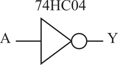
Figure 3.1.1. A NOT gate.
The typical propagation delay time (tpd) for this not gate is 8 ns. Considering just the typical delay, we specify the time when Y rises in terms of the time when A falls. That is
↑Y = ↓A + tpd = ↓A + 8
From the 74HC04 data sheet, we see the maximum propagation delay is 15 ns, and no minimum is given. Since the delay cannot be negative, we set the minimum to zero and write
↑Y = [↓A, ↓A + 15] = ↓A + [0, 15]
We specify the time interval when Y is high as
(↑Y, ↓Y) = ( [↓A, ↓A+15], [↑A, ↑A+15] ) = (↓A+[0,15], ↑A+[0,15] )
: Read the 74HC00 data sheet. Assume B is high. Initially A is low and Y is high. Then A goes high (Y goes low) and then A goes low (Y goes high again). Determine the timing interval when the output Y is low. See page 9 of the data sheet, assume Vcc=2V.
Positive logic means the true or asserted state is a higher voltage than the false or not asserted state. Negative logic means the true or asserted state is a lower voltage than the false or not asserted state. The * in the name G* means negative logic. Other syntax styles that mean negative logic include a slash before the symbol (e.g., \G), the letter n in the name (Gn), or a line over the top of the symbol.
Next, we will consider the timing of a tristate driver, as shown in Figure 3.1.2. There are eight data inputs to the 74HC244, labeled as A. Its eight data outputs are labeled Y. The 74HC244 tristate driver has two modes. When the output enable, G*, is low, the output Y equals the input A. When G* is high, the output Y floats, meaning it is not driven high or low. The slash with an 8 over top means there are eight signals that all operate in a similar or combined fashion. See the data sheet for the 74HC244
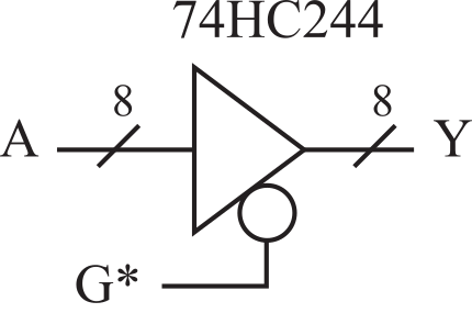
Figure 3.1.2. A tristate driver.
For the 74HC244 timing, we will assume the input A is stable and consider the relationship between input G* and the output Y. The data available interval is defined as when the data driven by an output will be valid. From its data sheet, the output of the 74HC244 is valid between 0 and 38 ns after the fall of G*. It will remain valid until 0 to 38 ns after the rise of G*. The data available interval is
DA = (↓G*+ ten, ↑G*+ tdis) = (↓G*+[0, 38], ↑G*+[0,38] )
: Read the 74HC125 data sheet. Assume the input A is stable. Initially, OE* is high. Then, OE* goes low (Y is driven) and then OE* goes high (Y goes hiZ). Determine the data available interval. See page 4 of the data sheet, assume Vcc=2V, and temperature is +25.
The 74HC374 octal D flip-flop has eight data inputs (D) and eight data outputs (Q), see Figure 3.1.3. A D flip-flip will store or latch its D inputs on the rising edge of its Clk input. The OE* input signal on the 74HC374 works in a manner like the 74HC244. When OE* is low, the stored values in the flip-flop are available at its Q outputs. When OE* is high, the Q outputs float. Making OE* go high or low does not change the internal stored values. OE* only affects whether the stored values are driven onto the Q outputs. See the data sheet for the 74HC374
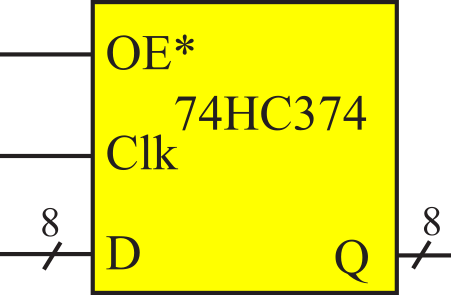
Figure 3.1.3. An octal D flip-flop.
The data required interval specifies when the data to be stored into the destination must be valid. The time before the clock the data must be valid is called the setup time. The setup time for the 74HC374 is 25 ns. The time after the clock the data must continue to be valid is called the hold time. The hold time for the 74HC374 is 5 ns. The data required interval is
DR = (↑Clk- tsu, ↑Clk+ th) = (↑Clk-25, ↑Clk+5)
: Read the 74HC74 data sheet. Which edge of the CLK writes into the flip flop? Hint: search for setup and hold.
When data are transferred from one location (the source) and stored into another (the destination), there are two time-intervals that will determine if the transfer will be successful. For a successful transfer the data available interval must overlap (start before and end after) the data required interval. Let a, b, c, d be times relative to the same zero-time reference, let the data available interval be (a, d), and let the data required interval be (b, c), as shown in Figure 3.1.4. The data will be successfully transferred if
a ≤ b and c ≤ d
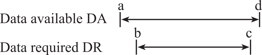
Figure 3.1.4. The data available interval should overlap the data required interval.
The example shown in Figure 3.1.5 illustrates the fundamental concept of timing for a digital interface. The objective is to transfer the data from the input, In, to the output, Out. First, we assume the signal at the In input of the 74HC244 is always valid. When the tristate control, G*, is low then the In is copied to the Bus. On the rising edge of Clk, the 74HC374 D flip-flop will copy this data to the output Out.
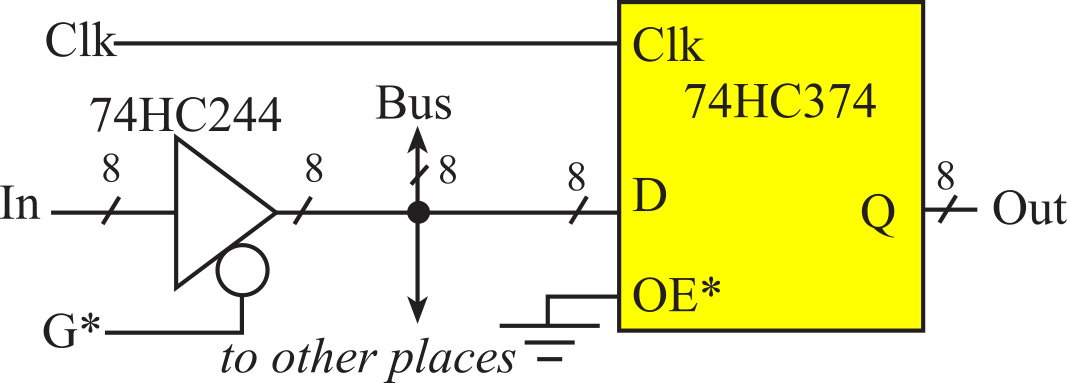
Figure 3.1.5. Simple circuit to illustrate that the data available interval should overlap the data required interval.
The data available interval defines when the signal Bus contains valid data and is determined by the timing of the 74HC244. Since the objective is to make the data available interval overlap the data required window, the worst-case situation will be the shortest data available and the longest data required intervals. Without loss of information, we can write the shortest data available interval as
DA = (↓G*+38, ↑G*)
The data required interval is determined by the timing of the 74HC374. The 74HC374 input, Bus, must be valid from 25 ns before the rise of Clk and remain valid until 5 ns after that same rise of Clk.
DR = (↑Clk-25, ↑Clk+5)
Thus, the data will be properly transferred if the following are true:
↓G*+38 ≤ ↑C-25 and ↑C+5 ≤ ↑G*
Notice in Figure 3.1.5, the signal between the 74HC244 and 74HC374 is labeled Bus. A bus is a collection of signals that facilitate the transfer of information from one part of the circuit to another. Consider a system with multiple 74HC244's and multiple 74HC374's. The Y outputs of all the 74HC244's and the D inputs of all the 74HC374's are connected to this bus. If the system wished to transfer from input 6 to output 5, it would clear G6* low, make Clk5 rise, and then set G6* high. At some point Clk5 must fall, but the exact time is not critical. One of the problems with a shared bus will be bus arbitration, which is a mechanism to handle simultaneous requests.
An alternative mechanism for describing when events occur uses voltage versus time graphs, called timing diagrams. It is very intuitive to describe timing events using graphs because it is easy to visually sort events into their proper time sequence. Figure 3.1.6 defines the symbols we will use to draw timing diagrams in this book. Arrows will be added to describe the causal relations in our interface. Numbers or variables can be included that define how far apart events will be or should be. It is important to have it clear in our minds whether we are drawing an input or an output signal, because what a symbol means depends on whether we are drawing the timing of an input or an output signal. Many datasheets use the tristate symbol when drawing an input signal to mean "don't care".
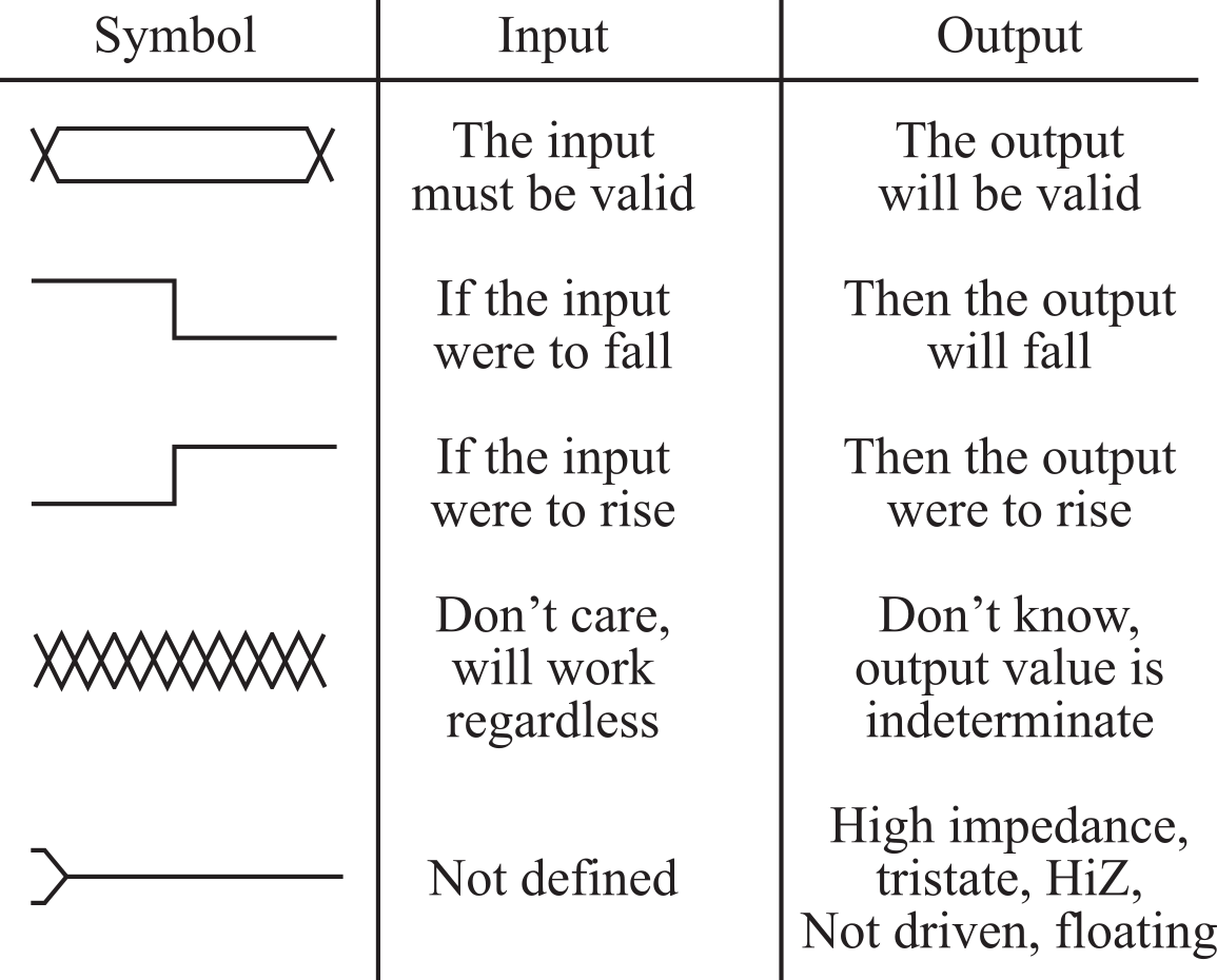
Figure 3.1.6. Nomenclature for drawing timing diagrams .
To illustrate the graphical relationship of dynamic digital signals, we will draw timing diagrams for the three devices presented in the last section, see Figure 3.1.7. The arrows in the 74HC04 timing diagram describe the causal behavior. If the input were to rise, then the output will fall tpHL time later. The subscript HL refers to the output changing from high to low. Similarly, if the input were to fall, then the output will rise tpLH time later.
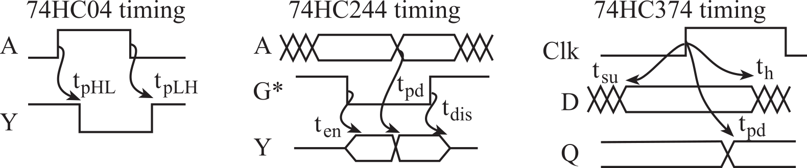
Figure 3.1.7. Timing diagrams for the circuits for the 74HC04, 74HC244 and 74HC374.
The arrows in the 74HC244 timing diagram also describe the causal behavior. If the input A is valid and if the OE* were to fall, then the output will go from floating to properly driven ten time later. If the OE* is low and if the input A were to change, then the output will change tpd time later. If the OE* were to rise, then the output will go from driven to floating tdis time later.
The parallel lines on the D timing of the 74HC374 mean the input must be valid. "Must be valid" means the D input could be high or low, but it must be correct and not changing. In general, arrows represent causal relationships (i.e., "this" causes "that"). Hence, arrows should be drawn pointing to the right, towards increasing time. The setup time arrow is an exception to the "arrows point to the right" rule. The setup arrow (labeled with tsu) defines how long before an edge the input must be stable. The hold arrow (labeled with th) defines how long after that same edge the input must continue to be stable.
The timing of the 74HC244 mimics the behavior of devices on the computer bus during a read cycle, and the timing of the 74HC374 clock mimics the behavior of devices during a write cycle. Figure 3.1.8 shows the timing diagram for the interface problem presented in Figure 3.1.5. Again, we assume the input In is valid at all times. The data available (DA) and data required (DR) intervals refer to data on the Bus. In this timing diagram, we see graphically the same design constraint developed with timing equations. ↓G*+38 must be less than or equal to ↑C‑25 and ↑C+5 must be less than or equal to ↑G*. One of the confusing parts about a timing diagram is that it contains more information than matters. For example, notice that the fall of C is drawn before the rise of G*. In this interface, the relative timing of ↑G* and ↓C does not matter. However, we draw ↓C so that we can specify the width of the C pulse must be at least 20 ns.
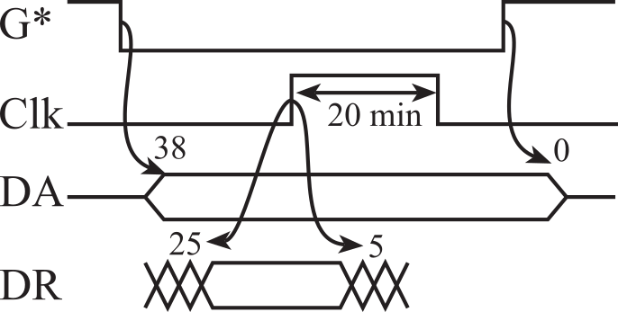
Figure 3.1.8. Timing diagram of the interface shown in Figure 3.1.5.
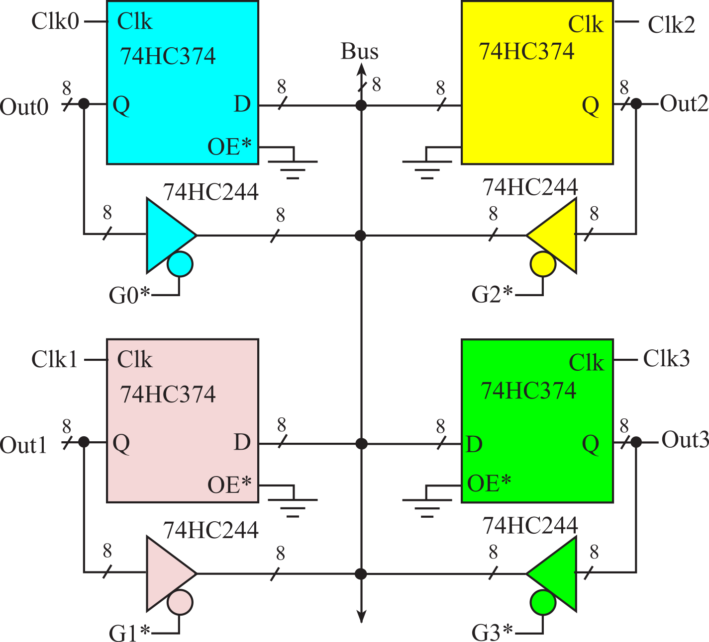
Figure 3.1.9. Digital system with four 8-bit registers.
: Consider the digital system in Figure 3.1.9 with timing of Figure 3.1.8. Assume all G* signals are initially high (all 74HC244 drivers are off. Assume all Clk signals are initially low. Describe the sequence of events needed to copy data from Out1 to Out2.
3.1.2. Universal Asynchronous Receiver Transmitter (UART)
The Universal Asynchronous Receiver Transmitter (UART) is a protocol that allows for data input or output. A frame is a complete and non-divisible packet of bits, see Figure 3.1.10. A frame includes both information (e.g., data, characters) and overhead (start bit, error checking, and stop bits.) A frame is the smallest packet that can be transmitted. The UART protocol has 1 start bit, 5-8 data bits, no/even/odd parity, and 1-2 stop bits. The idle level is true (3.3V). The start bit is false (0V.) A true data bit is 3.3V, and a false data bit is +0V.
Observation: The UART protocol always has one start bit and at least one stop bit.
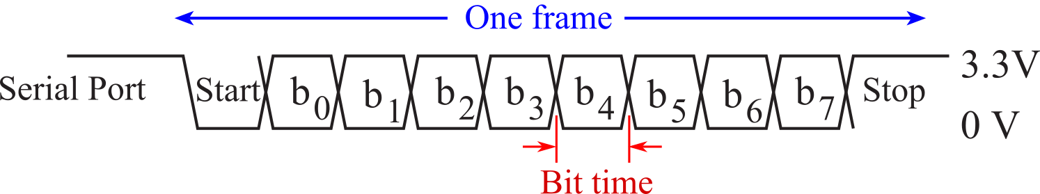
Figure 3.1.10. A UART frame showing 1 start, 8 data, no parity, and 1 stop bit.
: If the UART protocol has eight data bits, no parity, and one stop bit, how many total bits are in a frame?
Figure 3.1.11 shows a device interfaced to the microcontroller using UART. There are three lines necessary to implement UART: TxD, RxD, and ground. Data flows out the TxD pin into the RxD pin, one bit at a time. Shift registers in each device implement the serial protocol.
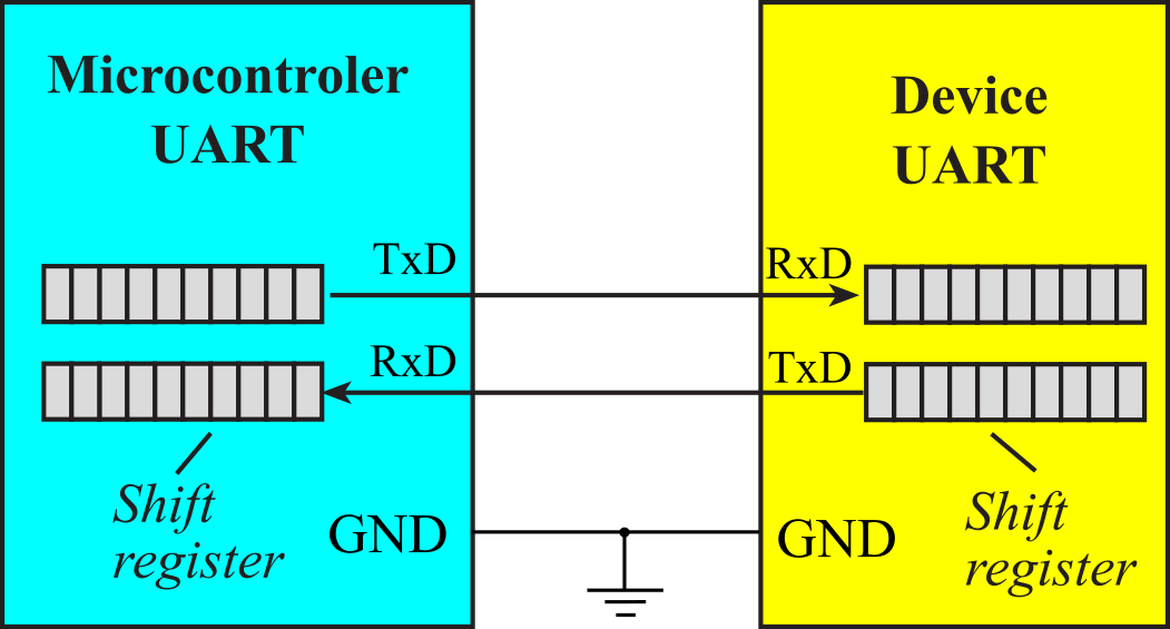
Figure 3.1.11. A UART shifts data from the transmit shift register into the receiver shift register. The clocks are not connected.
Parity can be used to detect errors. Parity is generated by the transmitter and checked by the receiver. For even parity, the number of ones in the data plus parity is an even number. For odd parity, the number of ones in the data plus parity is an odd number. When the microcontroller and the peripheral are in the same enclosure, errors are unlikely. In this situation, we will operate without parity because it is simpler. If the communication channel were to go from one enclosure to another, through a noisy environment, we would use RS232 or RS422 interface drivers, and then consider adding parity to detect errors.
The bit time is the basic unit of time used in serial communication. It is the time between each bit. The transmitter outputs a bit, waits one bit time, and then outputs the next bit. The start bit is used to synchronize the receiver with the transmitter. The receiver waits on the idle line until a start bit is first detected. After the true to false transition, the receiver waits a half of a bit time. The half of a bit time wait places the input sampling time in the middle of each data bit, giving the best tolerance to variations between the transmitter and receiver clock rates. To operate properly the data available interval must overlap the data required interval ( see Section 3.1.1. Timing Diagrams). Next, the receiver reads one bit every bit time. The baud rate is the total number of bits (information, overhead, and idle) per time.
baud rate = 1/(bit time)
We will define information as
the data that the "user" intends to be transmitted by the communication system.
Examples of information include
- Characters to be printed on your printer
- A picture file to be transmitted to another computer
- A digitally encoded voice message communicated to your friend
- The object code file to be downloaded from the PC to the microcontroller
We will define overhead
as signals added to the communication to affect reliable transmission.
Examples of overhead include
- Start bit(s) start byte(s) or start code(s)
- Stop bit(s) stop byte(s) or stop code(s)
- Error checking bits like parity
Bandwidth, latency, and reliability are the fundamental performance measures for a communication system. Although, in a general sense overhead signals contain "information", overhead signals are not included when calculating bandwidth or considering full duplex, half duplex, and simplex. In similar way, if we are sending 2 bits of data, but add 6 bits of zeros to fill the byte field in the frame, we consider that there are 2 bits of information per frame (not 8 bits.) We will use the three terms bandwidth, bit rate and throughput interchangeably to specify the number of information bits per time that are transmitted. For UART communication systems, we can calculate the maximum bandwidth as:
Bandwidth = (number of information bits/frame)*(Baud rate)/(total number of bits/frame)
: Consider a UART system with no parity. Does adding parity, while keeping the baud rate fixed, affect maximum bandwidth?
Latency is the time delay between when a message is sent and when it is received. For the simple systems in this chapter, at the physical layer, latency can be calculated as the frame size in bits divided by the baud rate in bits/sec. For example, a UART protocol with 10-bit frames running at 9600-bps baud rate will take 1.04 ms (10bits/9600bps) to go from transmitter to receiver.
Reliability is defined as the probability of corrupted data or the mean time between failures (MTBF). One of the confusing aspects of bandwidth is that it could mean two things. The peak bandwidth is the maximum achievable data transfer rate over short periods during times when nothing else is competing for resources. When we say the bandwidth of a serial channel with 10-bit frames and a baud rate of 9600 bps is 960 bytes/s, we are defining peak bandwidth. At the component level, it is appropriate to specify peak bandwidth. However, on a complex system, there will be delays caused by the time it takes software to run, and there will be times when the transmission will be stalled due to conditions like full or empty FIFOs. The sustained bandwidth is the achievable data transfer rate over long periods of time and under typical usage and conditions. At the system level, it is appropriate to specify sustained bandwidth.
The design parameters that affect bandwidth are resistance, capacitance and power. It takes energy to encode each bit, therefore the bandwidth in bits per second is related to the power, which is energy per second. Capacitance exists because of the physical proximity of the wires in the cable. The time constant τ of a simple RC circuit is R*C. An increase in capacitance will decrease the slew rate (dV/dt) of the signal (see Figure 3.1.12), limiting the rate at which signals can change, thereby reducing the bandwidth of the digital transmission. However, we can increase the slew rate by using more power. We can increase the energy over the same time period by increasing voltage, increasing current, or decreasing resistance.
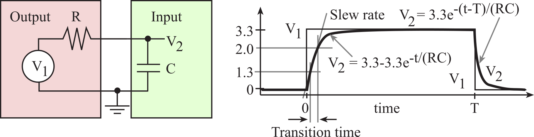
Figure 3.1.12. Capacitance loading is an important factor when interfacing CMOS devices.
Observation: Communication system transmit energy across distance. Digital storage systems transmit energy across time.
A full duplex communication system allows information (data, characters) to transfer simultaneously in both directions. A full duplex channel allows bits (information, error checking, synchronization or overhead) to transfer simultaneously in both directions.
: Why is the system in Figure 3.1.11 full duplex?
A half duplex communication system allows information to transfer in both directions, but in only one direction at a time. Half duplex is a term usually defined for modem communications, but in this book, we will expand its meaning to include any serial protocol that allows communication in both directions, but only one direction at a time. A fundamental problem with half duplex is the detection and recovery from a collision. A collision occurs when both computers simultaneously transmit data. Fortunately, every transmission frame is echoed back into its own receiver. The transmitter program can output a frame, wait for the frame to be transmitted (which will be echoed into its own receiver) then check the incoming parity and compare the data to detect a collision. If a collision occurs, then it will probably be detected by both computers. After a collision, the transmitter can wait awhile and retransmit the frame. The two computers need to decide which one will transmit first after a collision so that a second collision can be avoided.
Observation: Most people communicate in half duplex.
A common hardware mechanism for half duplex utilizes open drain logic. The microcontroller open drain mode has two output states: zero and HiZ.
: What is the difference between full duplex and half duplex?
A simplex communication system allows information to transfer only in one direction.
To transfer information correctly, both sides of the channel must operate at the same baud rate. In an asynchronous communication system, the two devices have separate and distinct clocks. Because these two clocks are generated separately (one on each side), they will not have exactly the same frequency or be in phase. If the two baud rate clocks have different frequencies, the phase between the clocks will also drift over time. Transmission will occur properly if the periods of the two baud rate clocks are close enough. The 3.3V to 0V edge at the beginning of the start bit is used to synchronize the receiver with the transmitter. If the two baud rate clock periods in a UART system differ by less than 5%, then after 10 bits the receiver will be off by less than half a bit time (and no error will occur.) Any larger difference between the two periods may cause an error.
Observation: Self-centered people employ simplex communication.
We must consider transmission line effects of long cables or high-speed communication. At high speeds, the slew rate must be very high. There is a correspondence between rise time (τ) of a digital signal and equivalent sinusoidal frequency (f). The derivative of A*sin(2πft) is 2πf*A*cos(2πft). The maximum slew rate of this sinusoid is 2πf*A. Approximating the slew rate as A/τ, we get a correspondence between f and τ
f = 1/τ
For example, if the rise time is 5 ns, the equivalent frequency is 200 MHz. Notice that this equivalent frequency is independent of baud rate. So even at a baud rate of 1000 bits/sec, if the rise time is 5 ns, then the signal has a strong 200 MHz frequency component! This will radiate EM noise at 200 MHz. To deal with this issue, we may have to limit the slew rate. A rise time of 1 μs will have frequency components less than 1 MHz. Electrical signals travel at about 0.6 to 0.9 times the speed of light. This velocity factor (VF) is a property of the cable. For example, VF for RG-6/U coax cable is 0.75, whereas VF is only 0.66 for RG-58/U coax cable. Using the slower 0.66 estimate, the speed is v = 2*108 m/s. According to wave theory, the wavelength is l = v/f. Estimating the frequency from rise time, we get
λ = v * τ
In our example, a rise time of 5 ns is equivalent to a wavelength of about 1 m. As a rule of thumb, we will consider the channel as a transmission line if the length of the wire is greater than l/4. Another requirement is for the diameter of the wire to be much smaller than the wavelength. In a transmission line, the signals travel down the wires as waves according to the wave equation. Analysis of the wave equation is outside the scope of this book. However, you need to know that when a wave meets a change in impedance, some of the energy will transmit (a good thing) and some of the energy will reflect (a bad thing). Reflections are essentially noise on the signal, and if large enough, they will cause bit errors in transmission. We can reduce the change in impedance by placing terminating resistors on both ends of a long high-speed cable. These resistors reduce reflections; hence they improve signal to noise ratio.
Observation: An interesting tradeoff occurs when considering slew rate. The higher the slew rate, the faster data can be communicated. On the other hand, higher slew rates radiate more EM noise and may cause transmission line affects if the length of the cable approaches ¼ wavelength of the high frequencies generated by the slew rate.
Details of the UART on the TM4C123 can be found in Section T.4.
3.1.3. Synchronous Transmission and Receiving using the SPI
In a synchronous communication system, the two devices share the same clock. Typically, a separate wire in the serial cable carries the clock. In this way, very high baud rates can be obtained. Another advantage of synchronous communication is that very long frames can be transmitted. Larger frames reduce the operating system overhead for long transmissions because fewer frames need to be processed per message.
: What is the difference between synchronous and asynchronous communication?
Most microcontrollers support the Serial Peripheral Interface or SPI. The fundamental difference between UART, which implements an asynchronous protocol, and SPI, which implements a synchronous protocol, is the way the clock is implemented. Two devices communicating with asynchronous serial interfaces (UART) operate at the same frequency (baud rate) but have two separate clocks. With UART, the clock is not included in the interface cable between devices. Two devices communicating with synchronous serial interfaces operate from the same clock. SPI operates the two shift registers using different edges of the same clock. With an SPI protocol, the clock signal is included in the interface cable between devices.
The SPI system can operate as a master or as a slave. Another name for master is controller, and another name for slave is peripheral. The channel can have one master and one slave, or it can have one master and multiple slaves. With multiple slaves, the configuration can be a star (centralized master connected to each slave), or a ring (each node has one receiver and one transmitter, where the nodes are connected in a circle.) The master initiates all data communication. The master creates the clock, and the slave devices use the clock to latch the data in and send data out.
The SPI protocol includes four I/O lines, see Figure 3.1.13. The slave select CS is a negative logic control signal from master to slave signal signifying the channel is active. The second line, SCLK, is a 50% duty cycle clock generated by the master. The MOSI (master out slave in) or PICO (peripheral in controller out) is a data line driven by the master and received by the slave. The MISO (master in slave out) or POCI (peripheral out controller in) is a data line driven by the slave and received by the master. To work properly, the transmitting device uses one edge of the clock to change its output, and the receiving device uses the other edge to accept the data. Details on SPI and example interfaces on the TM4C123 can be found in Section T.5.
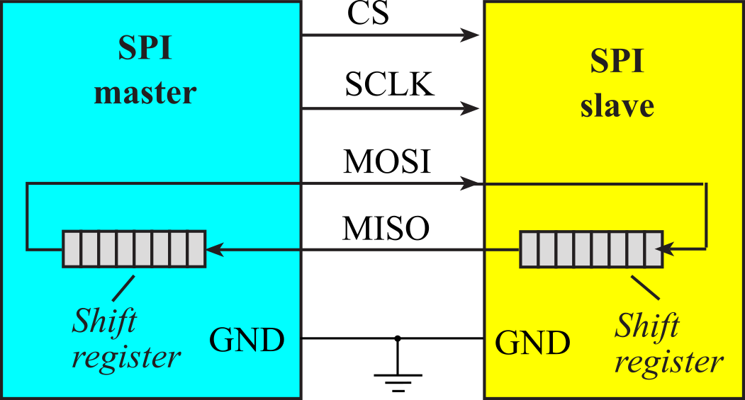
Figure 3.1.13. Serial Peripheral Interface uses synchronous communication.
Figure 3.1.14 shows the timing of one bit. The master drives the clock. At the points labeled T, the master changes its output (MOSI or PICO). S5 is propagation delay in the master from the edge of the clock to the change in MOSI. At the points labeled R, the slave reads its input (MISO or POCI). su is the setup time, which is the time before the clock that the data must be stable. hold is the hold time, which is the time after that same clock that the data must remain stable. The software initialization will select which edge to output and which edge to input, but it always uses different edges to input and output.
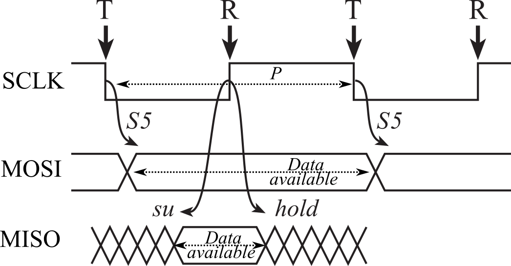
Figure 3.1.14. Timing at the master.
The data available is the time interval data will be driven on the line by the output device. The data required is the time interval data must be driven for the input device to properly receive the data. Let P be the period of the SCLK. S5 is a timing parameter of the master. su and hold are timing parameters in the slave. Arbitrarily, we define the time of the first T in Figure 3.1.14 to be 0. The start of the data available interval is at time S5. The start of the data required interval is ½P-su. The end of the data available interval is P+S5. The end of the data required interval is ½P+hold. If a timing parameter has a minimum and maximum, we choose the values that make data available shortest and make data required longest.
Data Available = (S5max, P+S5min)
Data Required = (½P-su, ½P+hold)
To operate, data available must overlap (start before and end after) data required. So, timing constraints are
S5max ≤ ½P-su and ½P+hold ≤ P+S5min
Observation: The reason SPI is fast and reliable is it uses one edge to output and the other edge to input.
Some peripheral devices simplify timing analysis by specifying the minimum clock period. Figure 3.1.15 shows some of the timing parameters for a TLV5616 DAC. For this DAC, the minimum SCLK high and SCLK low durations are 25ns, so the minimum period P is 50ns. Thus, the maximum SCLK frequency is 20 MHz.
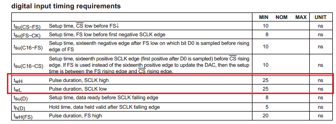
Figure 3.1.15. Timing parameters for a TLV5616 DAC.
: What are the setup and hold times of a TLV5616 DAC?
If the distance between the SPI devices is large (e.g., 1 meter), one should consider the transmission delays caused by speed of electrical transmission. Consider the situation in Figure 3.1.13 where the SCLK travels down a 1-m cable to the slave, and then MISO data must travel the 1-m cable back to the master. The propagation delay is the time required for the SCLK signal to pass from master to slave and the data to return from slave to master along the MISO line. Electrical signals travel about 0.6 to 0.9 times the speed of light. The velocity factor (VF) is the ratio of the speed relative to the speed of light. With a VF=0.6, and a cable length of 1 meter, the propagation delay will be
2*1m/(0.6*3*108m/sec) = 11ns
This 11-ns delay will limit the maximum communication rate.
: What would be the timing delay caused by a 10-meter cable?
Observation: In a simplex interface like the TLV5616 DAC, having only MOSI and no MISO, the length of the cable does not affect timing, because the SCLK and MOSI are delayed to the same amount. There will be capacitive affects of a long cable as shown in Figure 3.1.12.
3.1.4. Inter-Integrated Circuit (I2C) Interface
Ever since microcontrollers have been developed, there has been a desire to shrink the size of an embedded system, reduce its power requirements, and increase its performance and functionality. Two mechanisms to make systems smaller are to integrate functionality into the microcontroller and to reduce the number of I/O pins. The inter-integrated circuit I2C interface was proposed by Philips in the late 1980s to connect external devices to the microcontroller using just two wires. The SPI interface has been very popular, but it takes 3 wires for simplex and 4 wires for full duplex communication. In 1998, the I2C Version 1 protocol become an industry standard and has been implemented into thousands of devices. The I2C bus is a simple two-wire bi-directional serial communication system that is intended for communication between microcontrollers and their peripherals over short distances. This is typically, but not exclusively, between devices on the same printed circuit board, the limiting factor being the bus capacitance. It also provides flexibility, allowing additional devices to be connected to the bus for further expansion and system development. The interface will operate at baud rates of up to 100 kbps with maximum capacitive bus loading. The module can operate up to a baud rate of 400 kbps provided the I2C bus slew rate is less than 100ns. The maximum interconnect length and the number of devices that can be connected to the bus are limited by a maximum bus capacitance of 400pF in all instances. These parameters support the general trend that communication speed can be increased by reducing capacitance. Version 2.0 supports a high-speed mode with a baud rate up to 2.4 MHz (supported by TM4C123).
Figure 3.1.16 shows a block diagram of a communication system based on the I2C interface. The master/slave network may consist of multiple masters and multiple slaves. The Serial Clock Line (SCL) and the Serial Data line (SDA) are both bidirectional. Each line is open drain, meaning a device may drive it low or let it float. A logic high occurs if all devices let the output float, and a logic low occurs when at least one device drives it low. The value of the pull-up resistor depends on the speed of the bus. 4.7 kΩ is recommended for baud rates below 100 kbps, 2.2 kΩ is recommended for standard mode, and 1 kΩ is recommended for fast mode.
: Why is the recommended pull-up resistor related to the bus speed?
: What does open drain mean?
The SCL clock is used in a synchronous fashion to communicate on the bus. Even though data transfer is always initiated by a master device, both the master and the slaves have control over the data rate. The master starts a transmission by driving the clock low, but if a slave wishes to slow down the transfer, it too can drive the clock low (called clock stretching). In this way, devices on the bus will wait for all devices to finish. Both address (from Master to Slaves) and information (bidirectional) are communicated in serial fashion on SDA.
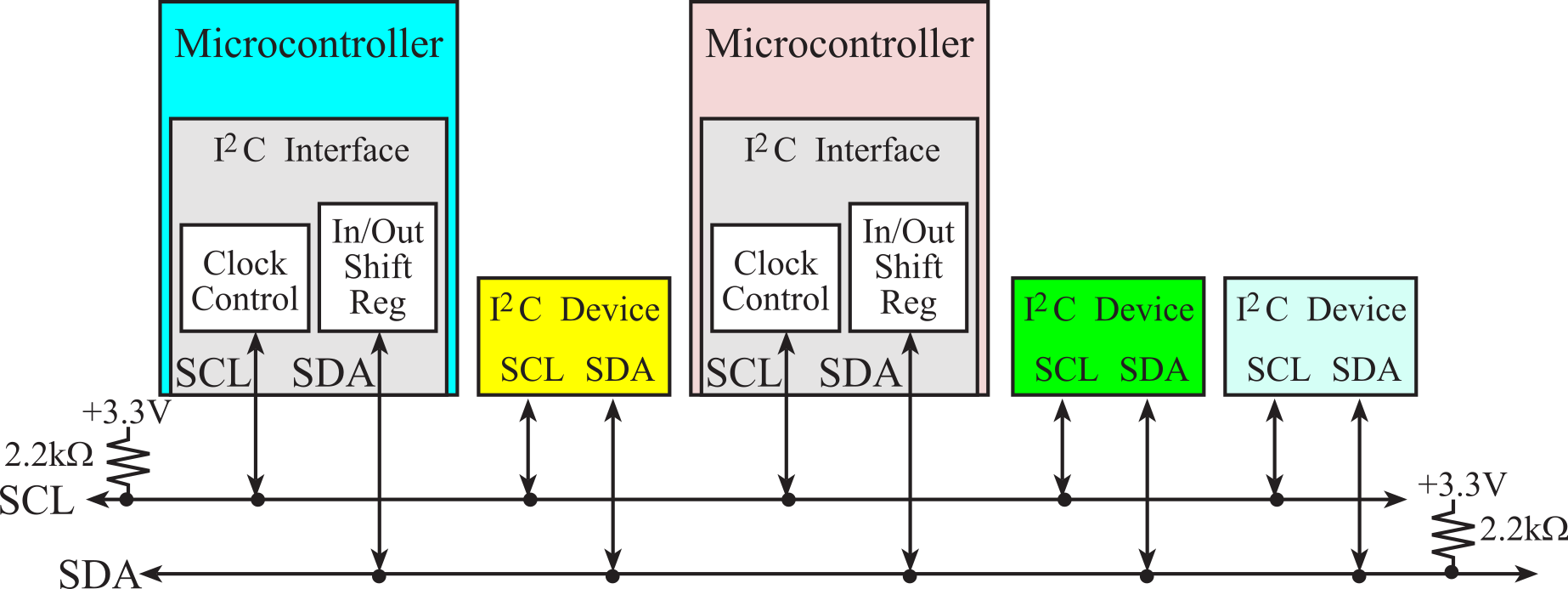
Figure 3.1.16. Block diagram of an I2C communication network Use 1kΩ resistors for fast mode.
The bus is initially idle where both SCL and SDA are both
high. This means no device is pulling SCL or SDA low. The communication on the
bus, which begins with a START and ends with a STOP, consists of five
components:
- START (S) is used by the master to initiate a transfer
- DATA is sent in 8-bit blocks and consists of
- 7-bit address and 1-bit direction from the master
- control code for master to slaves
- information from master to slave
- information from slave to master
- ACK (A) is used by slave to respond to the master after each 8-bit data transfer
- RESTART (R) is used by the master to initiate additional transfers without releasing the bus
- STOP (P) is used by the master to signal the transfer is complete and the bus is free
The basic timings for these components are drawn in Figure 3.1.17. For now, we will discuss basic timing, but we will deal with issues like stretching and arbitration later. A slow slave uses clock stretching to give it more time to react, and masters will use arbitration when two or more masters want the bus at the same time. An idle bus has both SCL and SDA high. A transmission begins when the master pulls SDA low, causing a START (S) component. The timing of a RESTART is the same as a START. After a START or a RESTART, the next 8 bits will be an address (7-bit address plus 1-bit direction). There are 128 possible 7-bit addresses, however, 32 of them are reserved as special commands. The address is used to enable a particular slave. All data transfers are 8 bits long, followed by a 1-bit acknowledge. During a data transfer, the SDA data line must be stable (high or low) whenever the SCL clock line is high. There is one clock pulse on SCL for each data bit, the MSB being transferred first. Next, the selected slave will respond with a positive acknowledge (Ack) or a negative acknowledge (Nack). If the direction bit is 0 (write), then subsequent data transmissions contain information sent from master to slave.
For a write data transfer, the master drives the RDA data line for 8 bits, then the slave drives the acknowledge condition during the 9th clock pulse. If the direction bit is 1 (read), then subsequent data transmissions contain information sent from slave to master. For a read data transfer, the slave drives the RDA data line for 8 bits, then the master drives the acknowledge condition during the 9th clock pulse. The STOP component is created by the master to signify the end of transfer. A STOP begins with SCL and SDA both low, then it makes the SCL clock high, and ends by making SDA high. The rising edge of SDA while SCL is high signifies the STOP condition.
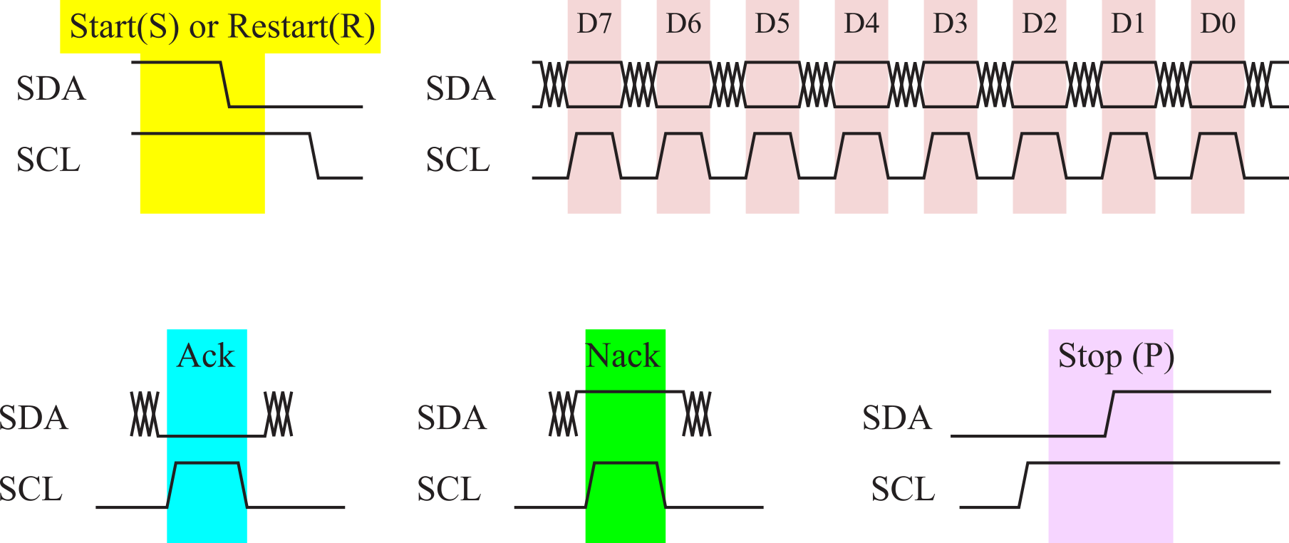
Figure 3.1.17. Timing diagrams of I2C components.
: What happens if no device sends an acknowledgement?
Figure 3.1.18 illustrates the case where the master sends 2 bytes of data to a slave. The shaded regions demark signals driven by the master, and the white areas show those times when the signal is driven by the slave. Regardless of format, all communication begins when the master creates a START component followed by the 7-bit address and 1-bit direction. In this example, the direction is low, signifying a write format. The 1st through 8th SCL pulses are used to shift the address/direction into all the slaves. In order to acknowledge the master, the slave that matches the address will drive the SDA data line low during the 9th SCL pulse. During the 10th through 17th SCL pulses sends the data to the selected slave. The selected slave will acknowledge by driving the SDA data line low during the 18th SCL pulse. A second data byte is transferred from master to slave in the same manner. In this particular example, two data bytes were sent, but this format can be used to send any number of bytes, because once the master captures the bus it can transfer as many bytes as it wishes. If the slave receiver does not acknowledge the master, the SDA line will be left high (Nack). The master can then generate a STOP signal to abort the data transfer or a RESTART signal to commence a new transmission. The master signals the end of transmission by sending a STOP condition.
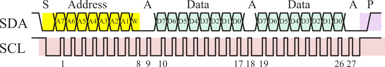
Figure 3.1.18. I2C transmission of two bytes from master to slave
Figure 3.1.19 illustrates the case where a slave sends 2 bytes of data the master. Again, the master begins by creating a START component followed by the 7-bit address and 1-bit direction. In this example, the direction is high, signifying a read format. During the 10th through 17th SCL pulses the selected slave sends the data to the master. The selected slave can only change the data line while SCL is low and must be held stable while SCL is high. The master will acknowledge by driving the SDA data line low during the 18th SCL pulse. Only two data bytes are shown in Figure 3.1.19, but this format can be used to receive as many bytes the master wishes. Except for the last byte all data are transferred from slave to master in the same manner. After the last data byte, the master does not acknowledge the slave (Nack) signifying 'end of data' to the slave, so the slave releases the SDA line for the master to generate STOP or RESTART signal. The master signals the end of transmission by sending a STOP condition.
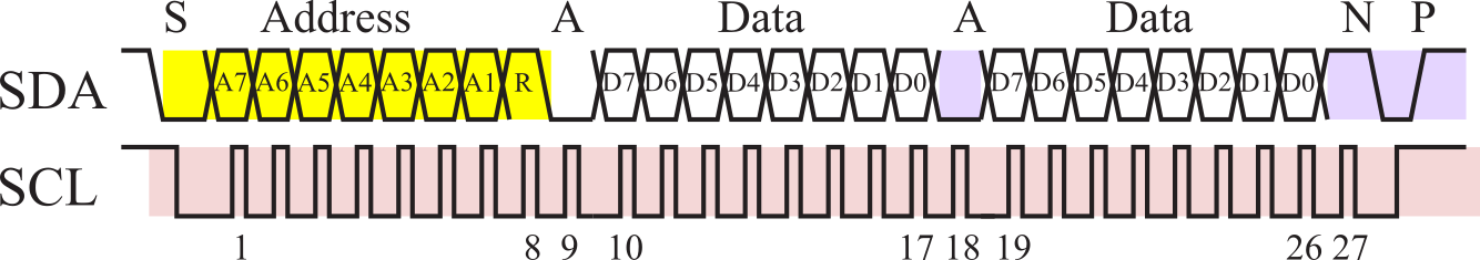
Figure 3.1.19. I2C transmission of two bytes from slave to master.
Figure 3.1.20 illustrates the case where the master uses the RESTART command to communicate with two slaves, reading one byte from one slave and writing one byte to the other. As always, the master begins by creating a START component followed by the 7-bit address and 1-bit direction. During the first start, the address selects the first slave, and the direction is read. During the 10th through 17th SCL pulses the first slave sends the data to the master. Because this is the last byte to be read from the first slave, the master will not acknowledge letting the SDA data float high during the 18th SCL pulse, so the first slave releases the SDA line. Rather than issuing a STOP at this point, the master issues a repeated start or RESTART. The 7-bit address and 1-bit direction transferred in the 20th through 27th SCL pulses will select the second slave for writing. In this example, the direction is low, signifying a write format. The 28th pulse will be used by the second slave pulls SDA low to acknowledge it has been selected. The 29th through 36th SCL pulses send the data to the second slave. During the 37th pulse the second slave pulls SDA low to acknowledge the data it received. The master signals the end of transmission by sending a STOP condition.
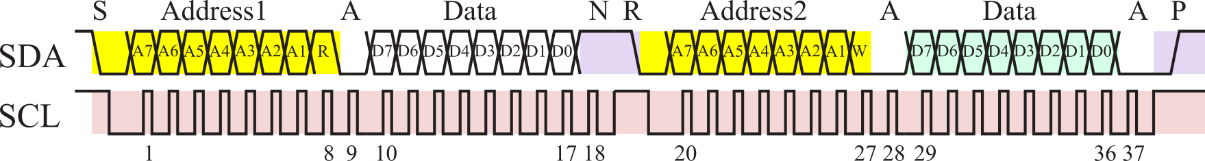
Figure 3.1.20. I2C transmission of one byte from the first slave and one byte to a second slave.
: Is I2C communication full duplex, half duplex, or simplex?
Table 3.1.1 lists some addresses that have special meaning. A write to address 0 is a general call address, and it is used by the master to send commands to all slaves. The 10-bit address mode gives two address bits in the first frame and 8 more address bits in the second frame. The direction bit for 10-bit addressing is in the first frame.
|
Address |
R/W |
Description |
|
0000 000 |
0 |
General call address |
|
0000 000 |
1 |
Start byte |
|
0000 001 |
x |
CBUS address |
|
0000 010 |
x |
Reserved for different bus formats |
|
0000 011 |
0 |
Reserved |
|
0000 1xx |
x |
High speed mode |
|
1111 0xx |
x |
10-bit address |
|
1111 1xx |
x |
Reserved |
Table 3.1.1. Special addresses used in the I2C network.
The I2C bus supports multiple masters. If two
or more masters try to issue a START command on the bus at the same time, both
clock synchronization and arbitration will occur. Clock synchronization
is procedure that will make the low period equal to the longest clock low
period and the high is equal to the shortest one among the masters. Figure 3.1.21
illustrates clock synchronization, where the top set of traces is generated by
the first master, and the second set of traces is generated by the second
master. Since the outputs are open drain, the actual signals will be the
wired-AND of the two outputs. Each master repeats these steps when it generates
a clock pulse. It is during step 3) that the faster device will wait for the
slower device
- Drive its SCL clock low for a fixed amount of time
- Let its SCL clock float
- Wait for the SCL to be high
- Wait for a fixed amount of time, stop waiting if the clock goes low
Because the outputs are open drain, the signal will be pulled to a logic high by the 2 kΩ resistor only if all devices release the line (output a logic high). Conversely, the signal will be a logic low if any device drives it low. When masters create a START, they first drive SDA low, then drive SCL low. If a group of masters are attempting to create START commands at about the same time, then the wire-AND of their SDA lines has its 1 to 0 transition before the wire-AND of their SCL lines has its 1 to 0 transition. Thus, a valid START command will occur causing all the slaves to listen to the upcoming address. In the example shown in Figure 3.1.21, Master #2 is the first to drive its clock low. In general, the SCL clock will be low from the time the first master drives it low (time 1 in this example), until the time the last master releases its clock (time 2 in this example.) Similarly, the SCL clock will be high from the time the last master releases its clock (time 2 in this example), until the time the first master drives its clock low (time 3 in this example.)
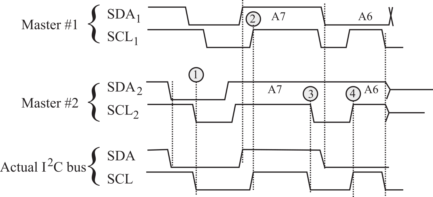
Figure 3.1.21. I2C timing illustrating clock synchronization and data arbitration.
The relative priority of the contending masters is determined by a data arbitration procedure. A bus master loses arbitration if it transmits logic "1" while another master transmits logic "0". The losing masters immediately switch over to slave receive mode and stop driving the SCL and SDA outputs. In this case, the transition from master to slave mode does not generate a STOP condition. Meanwhile, a status bit is set by hardware to indicate loss of arbitration. In the example shown in Figure 3.1.21, master #1 is generating an address with A7=1 and A6=0, while master #2 is generating an address with A7=1 and A6=1. Between times 2 and 3, both masters are attempting to send A7=1, and notice the actual SDA line is high. At time 4, master #2 attempts to make the SDA high (A6=1), but notices the actual SDA line is low. In general, the master sending a message to the lowest address will win arbitration.
: If Master 1 sends address 0x30 and Master 2 sends address #0x0F, which one wins arbitration?
The third synchronization mechanism occurs between master and slave. If the slave is fast enough to capture data at the maximum rate, the transfer is a simple synchronous serial mechanism. In this case the transfer of each bit from master to slave is illustrated by the following interlocked sequences.
Master sequence Slave sequence (no stretch)
1. Drive its SCL clock low
2. Set the SDA line
3. Wait for a fixed amount of time
4. Let its SCL clock float
5. Wait for the SCL to be high
6. Wait for a fixed amount of time 6. Capture SDA data on low to high edge of SCL
7. Stop waiting if the clock goes low
If the slave is not fast enough to capture data at the maximum rate, it can perform an operation called clock stretching. If the slave is not ready for the rising edge of SCL, it will hold the SCL clock low itself until it is ready. Slaves are not allowed to cause any 1 to 0 transitions on the SCL clock, but rather can only delay the 0 to 1 edge. The transfer of each bit from master to slave with clock stretching is illustrated by the following sequences
Master sequence Slave sequence (clock stretching)
1. Drive its SCL clock low 1. Wait for the SCL clock to be low
2. Set the SDA line 2. Drive SCL clock low
3. Wait for a fixed amount of time 3. Wait until it's ready to capture
4. Let its SCL clock float 4. Let its SCL float
5. Wait for the SCL clock to be high 5. Wait for the SCL clock to be high
6. Wait for a fixed amount of time 6. Capture the SDA data
7. Stop waiting if the clock goes low
Clock stretching can also be used when transferring a bit from slave to master
Master sequence Slave sequence (clock stretching)
1. Drive its SCL clock low 1. Wait for the SCL clock to be low
2. Wait for a fixed amount of time 2. Drive SCL clock low
3. Wait until next data bit is ready
4. Let its SCL clock float 4. Let its SCL float
5. Wait for the SCL clock to be high 5. Wait for the SCL clock to be high
6. Capture the SDA input
7. Wait for a fixed amount of time,
8. Stop waiting if the clock goes low
Observation: Clock stretching allows fast and slow devices to exist on the same I2C bus Fast devices will communicate quickly with each other, but slow down when communicating with slower devices.
: Arbitration continues until one master sends a zero while the other sends a one. What happens if two masters attempt to send data to the same address?
: Consider an I2C interface from the perspective of the processor (ignoring the pull up resistor). How much energy is there in the SCLK signal when the clock is low? How much energy is there in the SCLK signal when the clock is high?
: How much energy is there in the SCLK signal when the clock is high?
3.1.5. Universal Serial Bus (USB)
The Universal Serial Bus (USB) is a host-controlled, token-based high-speed serial network that allows communication between many of devices operating at different speeds. The objective of this section is not to provide all the details required to design a USB interface, but rather it serves as an introduction to the network. There is 650-page document on the USB standard, which you can download from http://www.usb.org. In addition, there are quite a few web sites setup to assist USB designers, such as the one titled "USB in a NutShell" at http://www.beyondlogic.org/usbnutshell/.
The standard is much more complex than the other networks
presented in this chapter. Fortunately, however, there are a number of USB
products that facilitate incorporating USB into an embedded system. In
addition, the USB controller hardware handles the low-level protocol. USB
devices usually exist within the same room, and are typically less than 4
meters from each other. USB 2.0 supports three speeds.
- High Speed - 480Mbits/s
- Full Speed - 12Mbits/s
- Low Speed - 1.5Mbits/s
The original USB version 1.1 supported just full speed mode and a low speed mode. The Universal Serial Bus is host-controlled, which means the host regulates communication on the bus, and there can only be one host per bus. On the other hand, the On-The-Go specification, added in version 2.0, includes a Host Negotiation Protocol that allows two devices negotiate for the role of host. The USB host is responsible for undertaking all transactions and scheduling bandwidth. Data can be sent by various transaction methods using a token-based protocol. USB uses a tiered star topology, using a hub to connect additional devices. A hub is at the center of each star. Each wire segment is a point-to-point connection between the host and a hub or function, or a hub connected to another hub or function, as shown in Figure 3.1.22. Because the hub provides power, it can monitor power to each device switching off a device drawing too much current without disrupting other devices. The hub can filter out high speed and full speed transactions so lower speed devices do not receive them. Because USB uses a 7-bit address, up to 127 devices can be connected.
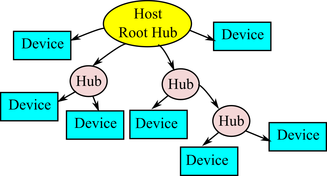
Figure 3.1.22. USB network topology.
The are four shielded wires (+5V power, D+, D- and ground). The D+ and D- are twisted pair differential data signals. It uses Non Return to Zero Invert (NRZI) encoding to send data with a sync field to synchronize the host and receiver clocks.
USB drivers will dynamically load and unload. When a device plugged into the bus, the host will detect this addition, interrogate the device and load the appropriate driver. Similarly, when the device is unplugged, the host will detect its absence and automatically unload the driver. The USB architecture comprehends four basic types of data transfers:
- Control Transfers: Used to configure a device at attach time and can be used for other device-specific purposes, including control of other pipes on the device.
- Bulk Data Transfers: Generated or consumed in relatively large quantities and have wide dynamic latitude in transmission constraints.
- Interrupt Data Transfers: Used for timely but reliable delivery of data, for example, characters or coordinates with human-perceptible echo or feedback response characteristics.
- Isochronous Data Transfers: Occupy a prenegotiated amount of USB bandwidth with a prenegotiated delivery latency. (Also called streaming real-time transfers).
Isochronous transfer allows a device to reserve a defined about of bandwidth with guaranteed latency. This is appropriate for real-time applications like in audio or video applications. An isochronous pipe is a stream pipe and is, therefore, always unidirectional. An endpoint description identifies whether a given isochronous pipe's communication flow is into or out of the host. If a device requires bidirectional isochronous communication flow, two isochronous pipes must be used, one in each direction.
A USB device indicates its speed by pulling either the D+ or D- line to 3.3 V, as shown in Figure 3.1.23. A pull-up resistor attached to D+ specifies full speed, and a pull-up resistor attached to D- means low speed. These device-side resistors are also used by the host or hub to detect the presence of a device connected to its port. Without a pull-up resistor, the host or hub assumes there is nothing connected. High speed devices begin as a full speed device (1.5k to 3.3V). Once it has been attached, it will do a high speed chirp during reset and establish a high speed connection if the hub supports it. If the device operates in high speed mode, then the pull-up resistor is removed to balance the line.
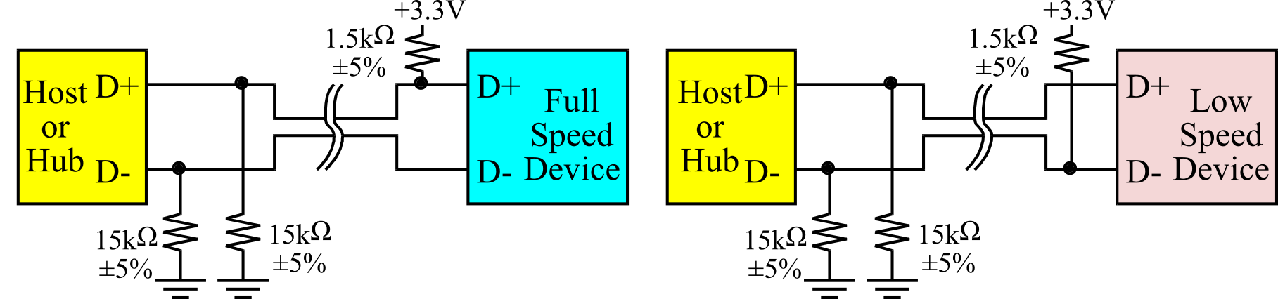
Figure 3.1.23. Pull-up resistors on USB devices signal specify the speed.
Like most communication systems, USB is made up of several layers of protocols. Like the CAN network presented earlier, the USB controllers will be responsible for establishing the low-level communication. Each USB transaction consists of three packets:
- Token Packet (header),
- Optional Data Packet, (information) and
- Status Packet (acknowledge)
The host initiates all communication, beginning with the Token Packet, which describes the type of transaction, the direction, the device address and designated endpoint. The next packet is generally a data packet carrying the information and is followed by a handshaking packet, reporting if the data or token was received successfully, or if the endpoint is stalled or not available to accept data. Data is transmitted least significant bit first. Some USB packets are shown in Figure 3.1.24. All packets must start with a sync field. The sync field is 8 bits long at low and full speed or 32 bits long for high speed and is used to synchronize the clock of the receiver with that of the transmitter. PID (Packet ID) is used to identify the type of packet that is being sent, as shown in Table 3.1.4.
The address field specifies which device the packet is designated for. Being 7 bits in length allows for 127 devices to be supported. Address 0 is not valid, as any device which is not yet assigned an address must respond to packets sent to address zero. The endpoint field is made up of 4 bits, allowing 16 possible endpoints. Low speed devices, however, can only have 2 additional endpoints on top of the default pipe. Cyclic Redundancy Checks are performed on the data within the packet payload. All token packets have a 5-bit CRC while data packets have a 16-bit CRC. EOP stands for End of packet. Start of Frame Packets (SOF) consist of an 11-bit frame number is sent by the host every 1ms ± 500ns on a full speed bus or every 125 μs ± 0.0625 μs on a high speed bus.

Figure 3.1.24. USB packet types.
|
Group |
PID Value |
Packet Identifier |
|
Token
|
0001 |
OUT Token, Address + endpoint |
|
1001 |
IN Token, Address + endpoint |
|
|
0101 |
SOF Token, Start-of-Frame marker and frame number |
|
|
1101 |
SETUP Token, Address + endpoint |
|
|
Data
|
0011 |
DATA0 |
|
1011 |
DATA1 |
|
|
0111 |
DATA2 (high speed) |
|
|
1111 |
MDATA (high speed) |
|
|
Handshake
|
0010 |
ACK Handshake, Receiver accepts error-free data packet |
|
1010 |
NAK Handshake, device cannot accept data or cannot send data |
|
|
1110 |
STALL Handshake, Endpoint is halted or pipe request not supported |
|
|
0110 |
NYET (No Response Yet from receiver) |
|
|
Special
|
1100 |
PREamble, Enables downstream bus traffic to low-speed devices. |
|
1100 |
ERR, Split Transaction Error Handshake |
|
|
1000 |
Split, High-speed Split Transaction Token |
|
|
0100 |
Ping, High-speed flow control probe for a bulk/control endpoint |
Table 3.1.4. USB PID numbers.
USB functions are USB devices that provide a capability or function such as a Printer, Zip Drive, Scanner, Modem or other peripheral. Most functions will have a series of buffers, typically 8 bytes long. Endpoints can be described as sources or sinks of data. As the bus is host centric, endpoints occur at the end of the communications channel at the USB function. The host software may send a packet to an endpoint buffer in a peripheral device. If the device wishes to send data to the host, the device cannot simply write to the bus as the bus is controlled by the host. Therefore, it writes data to endpoint buffer specified for input, and the data sits in the buffer until such time when the host sends a IN packet to that endpoint requesting the data. Endpoints can also be seen as the interface between the hardware of the function device and the firmware running on the function device.
While the device sends and receives data on a series of endpoints, the client software transfers data through pipes. A pipe is a logical connection between the host and endpoint(s). Pipes will also have a set of parameters associated with them such as how much bandwidth is allocated to it, what transfer type (Control, Bulk, Iso or Interrupt) it uses, a direction of data flow and maximum packet/buffer sizes. Stream Pipes can be used send unformatted data. Data flows sequentially and has a pre-defined direction, either in or out. Stream pipes will support bulk, isochronous and interrupt transfer types. Stream pipes can either be controlled by the host or device. Message Pipes have a defined USB format. They are host-controlled, which are initiated by a request sent from the host. Data is then transferred in the desired direction, dictated by the request. Therefore, message pipes allow data to flow in both directions but will only support control transfers.
The 12 independent signals are duplicated to achieve rotational symmetry, see Figure 3.1.25. Two sets of TX and RX pairs are available. A multiplexor is used to connect the output of one device to the input of the other. The pair TX1+ and TX1- combine to create SuperSpeed differential pair transmission. The CC1 and CC2 pins are channel configuration pins. They are used to detect cable attachment, removal, orientation, and current advertisement. The SBU1 and SBU2 pins correspond to low-speed signals used in some alternate modes. The USB-C cable can be used in USB 2.0 mode using D+, D-, VBUS, and GND.
The USB-C standard will negotiate and choose an appropriate voltage level and current flow on VBUS. It can handle up to 5A at 20V, which is 100W.
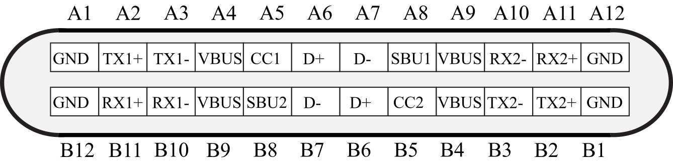

Figure 3.1.25. USB-C pin connections.
For more information, see
https://www.szapphone.com/blog/usb-c-pinout-guide/
There are two approaches to
implementing a USB interface for an embedded system. In the modular approach,
we will employ a USB-to-parallel, or USB-to-serial converter. The modular
approach is appropriate for adding USB functionality to an existing system. For
about $30, we can buy a converter cable with a USB interface to connect to the
personal computer (PC) and a serial interface to connect to the embedded
system, as shown in Figure 3.1.26. The embedded system hardware and software is
standard RS232 serial. These systems come with PC device drivers so that the
USB-serial-embedded system looks like a standard serial port (COM) to the PC
software. The advantage of this approach is that software development on the PC
and embedded system is simple. The disadvantage of this approach is none of the
power and flexibility of USB is utilized. In particular, the bandwidth is
limited by the RS232 line, and the data stream is unformatted. Similar products
are available that convert USB to the parallel port. Companies that make these
converters include
- FTDI https://ftdichip.com
- infineon https://www.infineon.com
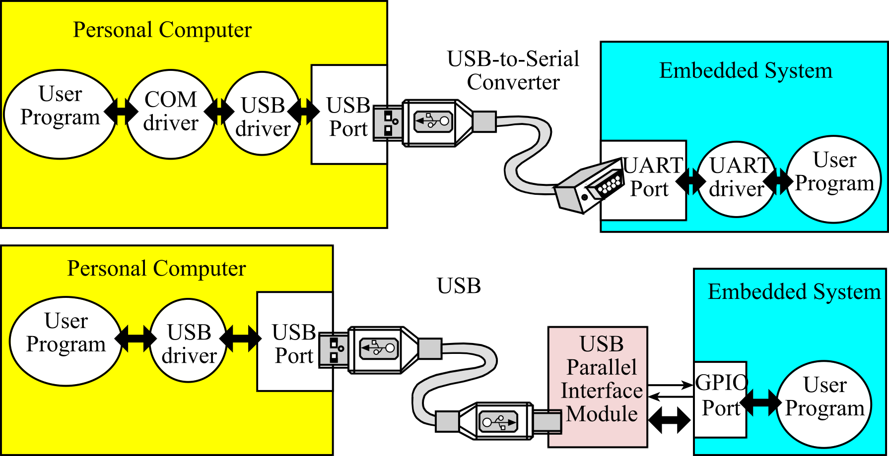
Figure 3.1.26. Modular approach to USB interfacing.
The second modular approach is
to purchase a USB interface module. These devices allow you to send
and receive data using parallel/serial handshake protocols. They typically include a USB-enabled microcontroller
and receiver/transmit FIFO buffers. This approach is more flexible than the
serial cable method, because both the microcontroller module and the USB
drivers can be tailored personalized. Some modules allow you to burn PID and
VID numbers into EEPROM. The advantages/disadvantages of this approach are like
the serial cable, in that the data is unformatted and you will not be able to
implement high bandwidth bulk transfers or negotiate for real-time bandwidth
available with isochronous data transfers. Companies that make these modules
include
- FTDI https://ftdichip.com/product-category/products/cables/usb-rs232-cable-series/
- Sparkfun https://www.sparkfun.com/catalogsearch/result/?q=serial+to+USB
- infineon https://www.infineon.com/cms/en/search.html#!term=USB%20serial%20bridge&view=all
A third approach to implementing a USB interface for an embedded system is to integrate the USB capability into the microcontroller itself. This method affords the greatest flexibility and performance, but requires careful software design on both the microcontroller and the host. Over the last 15 years USB has been replacing RS232 serial communication as the preferred method for connecting embedded systems to the personal computer. Manufacturers of microcontrollers have introduced versions of the product with USB capability. Every company that produces microcontrollers has members of the family with USB functionality. Examples include the Microchip PIC18F2455, Atmel AT89C5131A, FTDI FT245BM, Freescale MCF51Jx, STMicrosystems STM32F102, Texas Instruments MSP430F5xx, and Texas Instruments TM4C123. Figure 3.1.27 shows the USB configuration on the EK-TM4C123GXL LaunchPad Evaluation Kit, which is capable of operating as a device, a host or on-the-go (OTG). To use USB populate R25 and R29 on the LaunchPad. The TivaWare software library has 14 example projects for this evaluation board, including serial port translator, secure digital card, mouse, and keyboard interface.
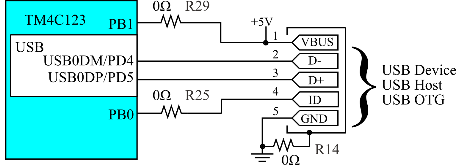
Figure 3.1.27. The TM4C123 LaunchPad kit supports USB host, device, and OTG modes.
To operate a USB interface at full speed DMA synchronization will be required, so that data is transferred directly from memory to USB output, or from USB input to memory.
3.2. Edge-triggered Interrupts
In this section we will present the general approach to
edge-triggered interrupts. We will show circuits with switches connected to
input pins, but in general edge-triggering can be used to interface any digital
input signal that has edges to which we want to recognize. The specific details
for the TM4C123 implementation can be Appendix T.7. On most
microcontrollers each of the GPIO input pins can be configured to generate
interrupts. For each input pin we choose to arm, we can select to interrupt on
- The rising edge of the pin
- The falling edge of the pin
- Either rising or falling edge of the pin
Typically, each of the ports has a separate interrupt service routine. Figure 3.2.1 shows two approaches to interfacing multiple switches using edge triggering. If there are fewer switches than ports, we can use the vectored approach and connect each switch to a pin on a separate port. In the vectored approach, each ISR uniquely identifies which pin triggered the interrupt. For the circuit on the left of Figure 3.2.1, the invocation of the PortA ISR means SW1 was triggered. On the other hand, the Port B ISR means SW2 was triggered.
On the other hand, if multiple switches are associated with the same module, it makes logical sense to connect them all to the same port. The polled approach, shown on the right of Figure 3.2.1 has switches connected to different pins on the same port. When an interrupt occurs, the ISR must poll the inputs to determine which pin(s) triggered. All MSPM0 edge-triggered interrupts invoke the same GROUP1_IRQHandler ISR, so polling is required.
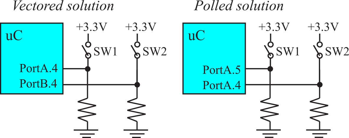
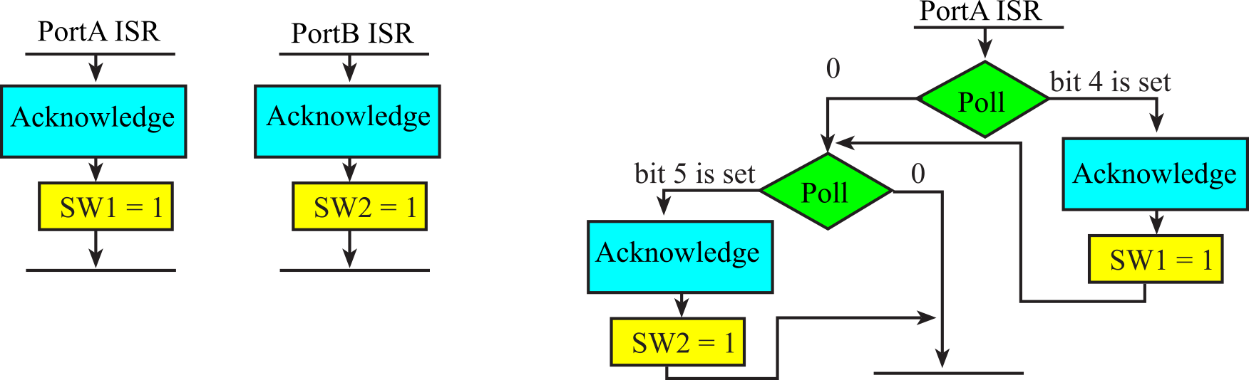
Figure 3.2.1. Circuits and flowcharts for interfacing multiple switches using edge triggering.
: In Figure 3.2.1 which edge should we arm to detect a switch touch?
: Is it possible to run code on both touch and release events?
Details of the edge-triggered interrupts on the TM4C123 can be found in Section T.7.
3.3. Touch Screens
3.3.1. Capacitive Touch Screen
A touchscreen works by detecting a change in
electrical charge when a finger touches its surface, which is coated with a
transparent conductive material like indium tin oxide (ITO); when touched, the
electrical field on the screen is disrupted, allowing the device to pinpoint
the location of the touch and register the input as a digital signal. Capacitive
touch screens are the most common type found in modern smartphones,
tablets, and many laptops. See Figure 3.3.1. They work based on electrical
properties and offer high sensitivity and clarity.
- The screen is coated with a transparent conductive material like indium tin oxide (ITO).
- The coating creates a uniform electrostatic field across the screen.
- Touching the screen disrupts the screen's electrostatic field.
- This disruption is measured as a change in capacitance.
- Software interprets this change and determines the location of the touch.
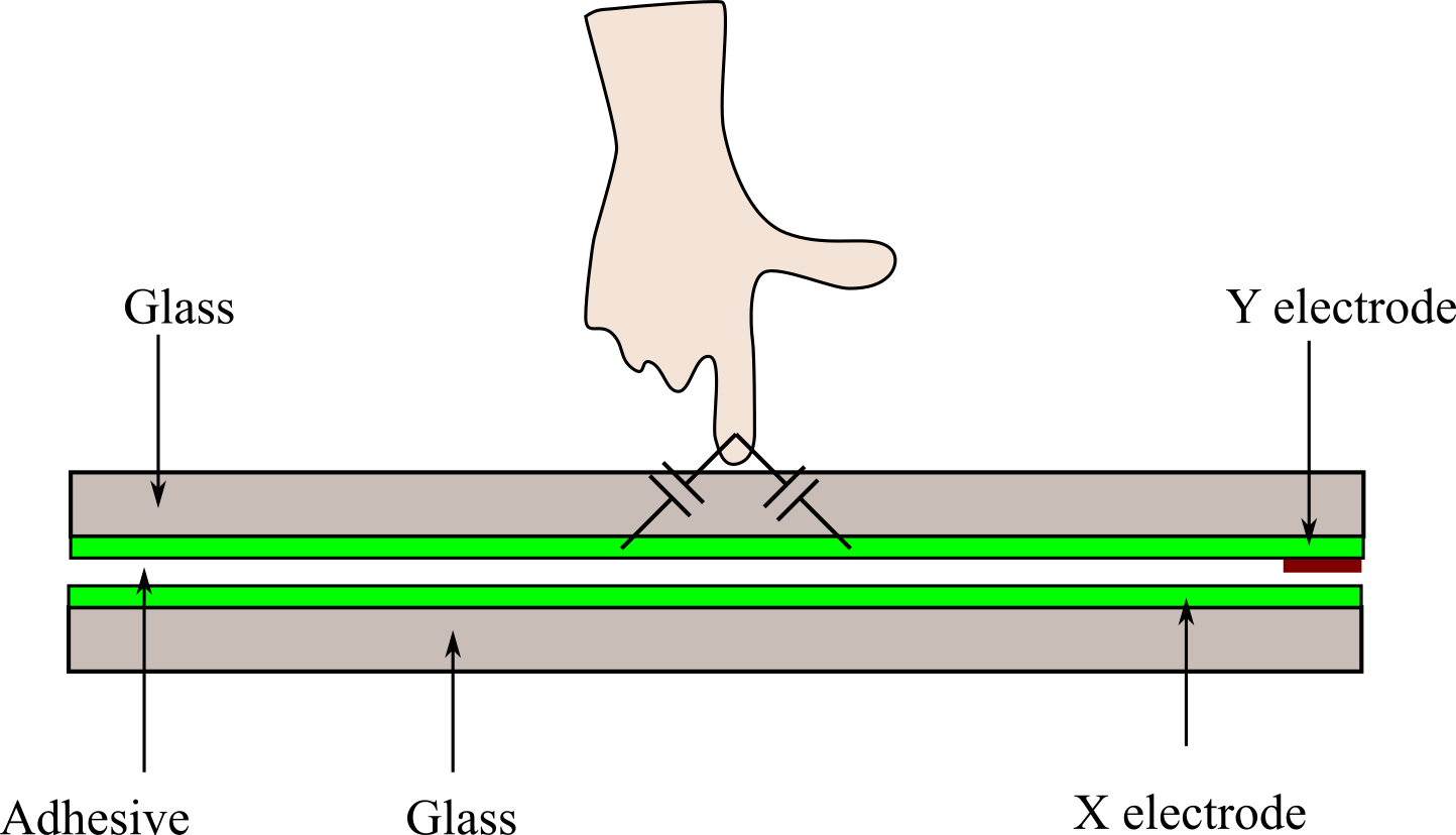
Figure 3.3.1. Capacitive touch screen.
Capacitive screens are known for their high
sensitivity, clarity, and ability to support multi-touch gestures. They work
well with bare fingers or conductive styluses but don't respond to
non-conductive objects like regular gloves or plastic styluses. Advantages of
capacitive screens include
Disadvantages of Capacitive Touch Screens
include
3.3.2. Resistive Touch Screen
Resistive touch screens are often found in harsh environments. They rely on pressure rather
than electrical conductivity. See Figure 3.3.2.
The scanning process is
- Make top and bottom GPIO outputs, make left and right analog inputs
- Make top 3.3V, make bottom 0V, sample ADC on left and right.
- Make top and bottom analog inputs, make left and right GPIO outputs
- Make left 3.3V, make right 0V, sample ADC on top and bottom.
- Convert ADC samples to (x,y) position.
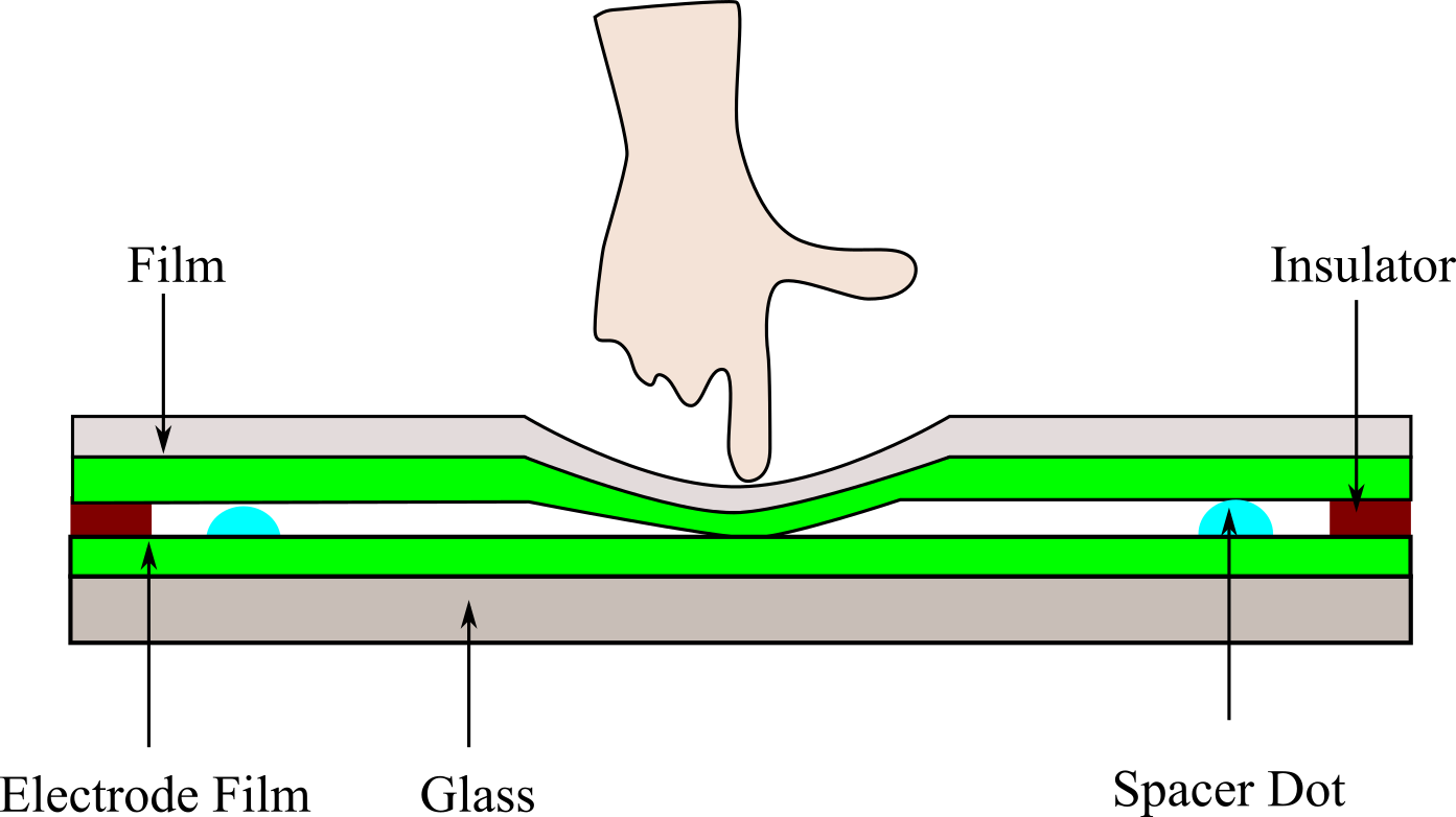
Figure 3.3.2. Resistive touch screen.
Resistive screens can be operated with any
object and are generally more durable, but they lack the sensitivity and
clarity of capacitive screens. Advantages include
- Can be used with any object (finger, stylus, gloved hand)
- Generally, less expensive than capacitive screens
- Work well in dusty or wet environments
Disadvantages of Resistive Touch Screens
include
- Less sensitive than capacitive screens
- Usually don't support multi-touch gestures
- Lower clarity due to multiple layers
Section 3.3 was derived from https://www.hp.com/us-en/shop/tech-takes/how-do-touch-screens-work
ezLCD is a family of displays that we will interface using UART, see Figure 3.3.3. Graphics and text are sent from microcontroller to display as serial output. Touch screen events are received by the microcontroller as serial input. See https://earthlcd.com/collections/ezlcd-intelligent-touchscreen-serial-lcds
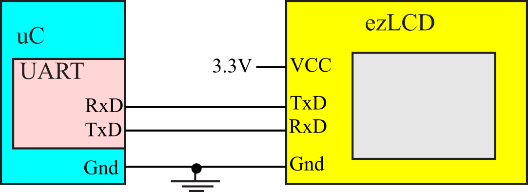
Figure 3.3.3. Integrated solution to a graphics display with touch screen.
: Which touch screen technology is best for medical applications?
: Which touch screen technology is best for military applications?
3.4. Keyboard Interfaces
In this section we attempt to interface switches to digital I/O pins and will consider three interfacing schemes, as shown in Figure 3.4.1. In a direct interface we connect each switch up to a separate microcontroller input pin. For example, using just one 8-bit parallel port, we can connect 8 switches using the direct scheme. An advantage of the direct interface is that the software can recognize all 256 (28) possible switch patterns. If the switches were remote from the microcontroller, we would need a 9-wire cable to connect it to the microcontroller. In general, if there are n switches, we would need n/8 parallel ports and n+1 wires in the cable. This method will be used when there are a small number of switches, or when we must recognize multiple simultaneous key presses. We will use the direct approach for music keyboards and for modifier keys such as shift, control, and alt.
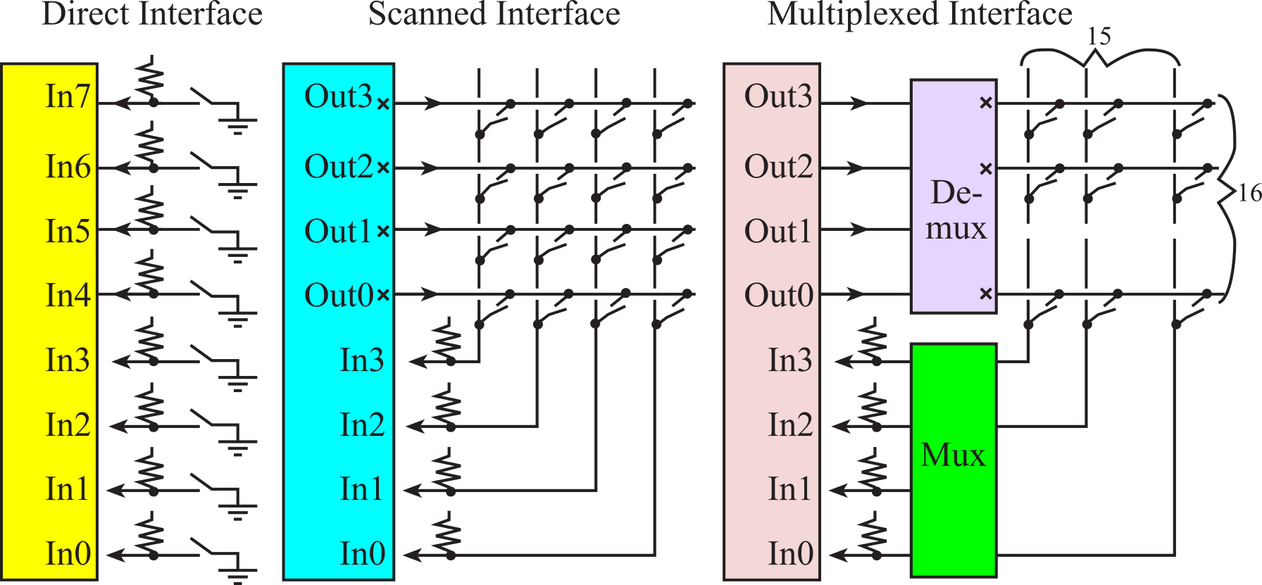
Figure 3.4.1. Three approaches to interfacing multiple keys.
In a scanned interface the switches are placed in a row/column matrix. The x at the four outputs signifies open drain (an output with two states: HiZ and low.) The software drives one row at a time to zero, while leaving the other rows at HiZ. By reading the column, the software can detect if a key is pressed in that row. The software "scans" the device by checking all rows one by one. Table 3.4.1 illustrates the sequence to scan the 4 rows.
|
Row |
Out3 |
Out2 |
Out1 |
Out0 |
|
3 |
0 |
HiZ |
HiZ |
HiZ |
|
2 |
HiZ |
0 |
HiZ |
HiZ |
|
1 |
HiZ |
HiZ |
0 |
HiZ |
|
0 |
HiZ |
HiZ |
HiZ |
0 |
Table 3.4.1. Scanning patterns for a 4 by 4 matrix keyboard.
For computers without an open drain output mode, the direction register can be toggled to simulate the two output states, HiZ/0, or open drain logic. This method can interface many switches with a small number of parallel I/O pins. In our example situation, the single 8-bit I/O port can handle 16 switches with only an 8-wire cable. The disadvantage of the scanned approach over the direct approach is that it can only handle situations where 0, 1 or 2 switches are simultaneously pressed. This method is used for most of the switches in our standard computer keyboard. The shift, alt, and control keys are interfaced with the direct method. We can "arm" this interface for interrupts by driving all the rows to zero. The edge-triggered input can be used to generate interrupts on touch and release. Because of the switch bounce, an edge-triggered interrupt will occur when any of the keys change. In this section we will interface the keypad using busy-wait synchronization.
With a scanned approach, we give up the ability to detect
three or more keys pressed simultaneously. If three keys are pressed in an "L"
shape, then the fourth key that completes the rectangle will appear to be
pressed. Therefore, special keys like the shift, control, option, and alt are
not placed in the scanned matrix, but rather are interfaced directly, each to a
separate input port. In general, an n by m matrix keypad has n*m
keys, but requires only n+m I/O pins. You can detect any 0, 1, or
2 key combinations, but it has trouble when 3 or more are pressed. The scanned
keyboard operates properly if
- No key is pressed
- Exactly one key is pressed
- Exactly two keys are pressed.
In a multiplexed interface, the computer outputs the binary value defining the row number, and a hardware decoder (or demultiplexer) will output a zero on the selected row and HiZ's on the other rows. The decoder must have open collector outputs (illustrated again by the x in the above circuit.) The computer simply outputs the sequence 0x00,0x10,0x20,0x30,...,0xF0 to scan the 16 rows, as shown in Table 3.4.2.
|
|
|
Computer output |
|
|
|
Decoder |
|
|
|||||
|
Row |
Out3 |
Out2 |
Out1 |
Out0 |
15 |
14 |
... |
0 |
|||||
|
15 |
1 |
1 |
1 |
1 |
0 |
HiZ |
|
HiZ |
|||||
|
14 |
1 |
1 |
1 |
0 |
HiZ |
0 |
|
HiZ |
|||||
|
... |
|
|
|
|
|
|
|
|
|||||
|
1 |
0 |
0 |
0 |
1 |
HiZ |
HiZ |
|
HiZ |
|||||
|
0 |
0 |
0 |
0 |
0 |
HiZ |
HiZ |
|
0 |
|||||
Table 3.4.2. Scanning patterns for a multiplexed 16 by 16 matrix keyboard.
In a similar way, the column information is passed to a hardware encoder that calculates the column position of any zero found in the selected row. One additional signal is necessary to signify the condition that no keys are pressed in that row. Since this interface has 16 rows and 16 columns, we can interface up to 256 keys! We could sacrifice one of the columns to detect the no key pressed in this row situation. In this way, we can interface 240 (15*16) keys on the single 8-bit parallel port. If more than one key is pressed in the same row, this method will only detect one of them. Therefore, we classify this scheme as only being able to handle zero or one key pressed.
Applications that can utilize this approach include touch screens and touch pads because they have a lot of switches but are only interested in the 0 or 1 touch situation. Implementing an interrupt driven interface would require too much additional hardware. In this case, periodic polling interrupt synchronization would be appropriate. In general, an n by m matrix keypad has n*m keys, but requires only x+y+1 I/O pins, where 2x = n and 2y = m. The extra input is used to detect the condition when no key is pressed.
TM4C123 example code can be found in Section T.1.4.
: How would you interface the 102 keys on a standard keyboard, ignoring the special keys like control, shift, alt, and function?
: How would you interface the special keys like control, shift, alt, and function on a standard keyboard?
3.5. Displays
3.5.1. ST7735R Display Interface
ST7735R is a low-cost color LCD graphics display, Figure 3.5.1.
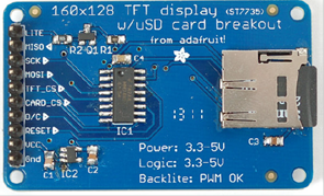
Figure 3.5.1. ST7735R graphics display with secure digital card (SDC) interface.
The details of the synchronous serial interface were presented in Section 3.1.2. Before we output data or commands to the display, we will check a status flag and wait for the previous operation to complete. Busy-wait synchronization is very simple and is appropriate for I/O devices that are fast and predicable. Running with an SCLK at 12 MHz means each transfer takes less than 1us.
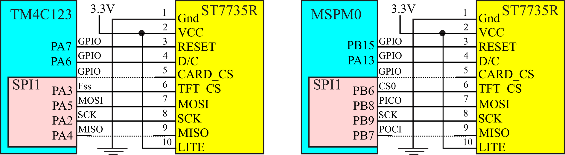
Figure 3.5.2. ST7735R display with 160 by 128 16-bit color pixels.
A block diagram of the interface is presented in Figure 3.5.3. The software writes into the data register, data passes through an 8-element hardware FIFO, and then each 8-bit byte is sent in serial fashion to the display. MOSI stands for master out slave in; the interface will send information one bit at a time over this line. SCK is the serial clock used to synchronize the shift register in the master and the shift register in the slave. TFT_CS is the chip select for the display; the interface will automatically make this signal low (active) during communication. D/C stands for data/command; software will make D/C high to send data and low to send a command.
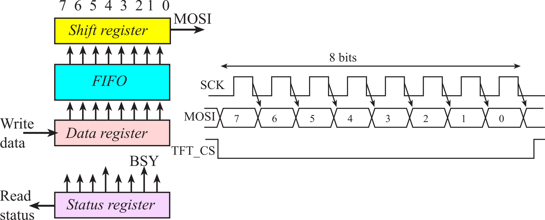
Figure 3.5.3. Block diagram and SPI timing for the ST7735R.
Writing an 8-bit command requires 4 steps.
1. Wait for the BUSY bit to be low.
2. Clear D/C to zero (configured for COMMAND).
3. Write the command to the data register.
4. Wait for the BUSY bit to be low.
The two busy-wait steps guarantee the command is completed before the software function returns. Writing an 8-bit data value also uses busy-wait synchronization. Writing an 8-bit data value requires 3 steps.
1. Wait for the transmit FIFO to have space.
2. Set D/C to one (configured for DATA).
3. Write the data to the data register.
The busy-wait step on "FIFO not full" means software can stream up to 8 data bytes without waiting for each data to complete.
Figure 3.5.4. ST7735R interface uses busy-wait synchronization.
: Why is busy-wait an appropriate synchronization for the ST7735R?
There is a rich set of graphics functions available for the ST7735R, allowing you to create amplitude versus time, or bit-mapped graphics. Refer to the ST7735R.h header file for more details. The (0,0) coordinate is the top left corner of the screen, and the (127,159) coordinate is the bottom right. See Figure 3.5.5. The prototype for drawing an image on the screen is
void ST7735_DrawBitmap(int16_t x, int16_t y, const uint16_t *image, int16_t w, int16_t h);
Figure 3.5.5 shows the position when placing a Bitmap on the screen. The coordinate (x,y) defines the lower left corner of the image. image is a pointer to the graphical image to draw. h and w are the height and width of the image.
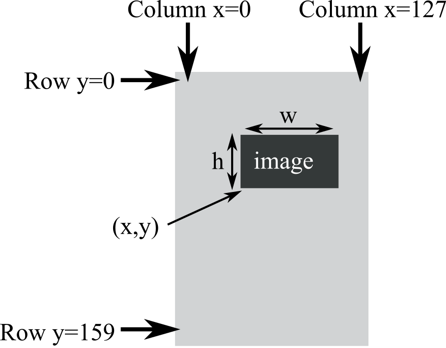
Figure 3.5.5. ST7735R graphics.
: Would DMA synchronization be appropriate for the ST7735R?
Details of the ST7735R-TM4C123 interface can be found in Section T.5.5.
3.5.2. SSD1306 Display Interface
Figure 3.5.6 shows the I2C protocol using with the SSD1306. Details of I2C programming on the TM4C123 can be found in Section T.6.
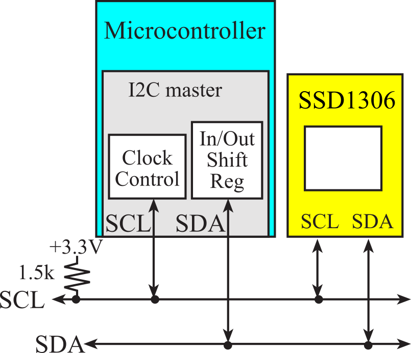
Figure 3.5.6. SSD1306 interface uses I2C protocol.
Figure 3.5.6 shows the interface between the microcontroller and the SSD1306. The SSD1306 has pullup resistors on both SCL and SDA, but we add an additional 1.5k resistor on the clock line to increase speed and reliability.
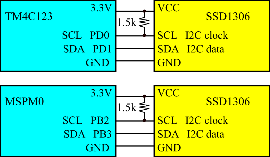
Figure 3.5.7. SSD1306 interface to the microcontroller.
There is a rich set of graphics functions available for the SSD1306, allowing you to create amplitude versus time, or bit-mapped graphics. Refer to the SSD1306.h header file for more details. The (0,0) coordinate is the top left corner of the screen, and the (127,63) coordinate is the bottom right. See Figure 3.5.7. The prototype for drawing an image on the screen is
void SSD1306_DrawBMP(uint8_t x, uint8_t y, const uint8_t *ptr, uint8_t threshold, uint16_t color);
Figure 3.5.7 shows the position when placing a Bitmap on the screen. The coordinate (x,y) defines the lower left corner of the image. ptr is a pointer to the graphical image to draw. The images have a 16-color BMP format. BMP images have the height and width encoded in the data. Because the images are 4-bit grey-scale and the display is black and white, threshold is used to map the 4-bit scale to 1-bit. color is black, white, or reverse.
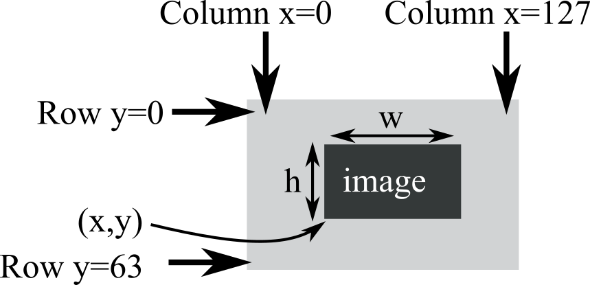
Figure 3.5.7. SSD1306 graphics for drawing a BMP image.
The prototype for printing a string on the screen is
void SSD1306_DrawString(int16_t x, int16_t y, char *pt, uint16_t color);
Figure 3.5.8 shows the position when drawing strings on the screen. The coordinate (x,y) defines the lower left corner of the string. pt is a pointer to the null-terminated string. color is black, white, or reverse.
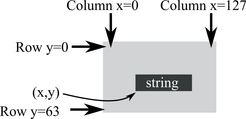
Figure 3.5.8. SSD1306 positioning for printing strings.
Details I2C on TM4C123 can be found in Section T.6.
3.5.3. Parallel LCD Interface
The previous displays used serial interfaces to connect the display to the microcontroller. There are many LCD displays using a parallel interface. Figure 3.5.9 shows the interface between the microcontroller and character display. This one is 1 row by 8 characters, but they can have up to 4 rows and be 40 characters wide. A software interface for this type of display can be found in the project LCD_4C123 and the file HD44780.h.
Writing an 8-bit command requires 8 steps using blind synchronization.
1. Clear R/W to zero to mean write
2. Clear RS to zero (COMMAND)
3. Write the command D7-D0
4. Wait 6us
5. Set E to one
6. Wait 6us
7. Clear E to zero
8. Wait 40us
Writing an 8-bit data value also uses blind synchronization. Writing an 8-bit data value requires a similar 8 steps.
1. Clear R/W to zero to mean write
2. Clear RS to one (data).
3. Write the data to D7-D0
4. Wait 6us
5. Set E to one
6. Wait 6us
7. Clear E to zero
8. Wait 40us
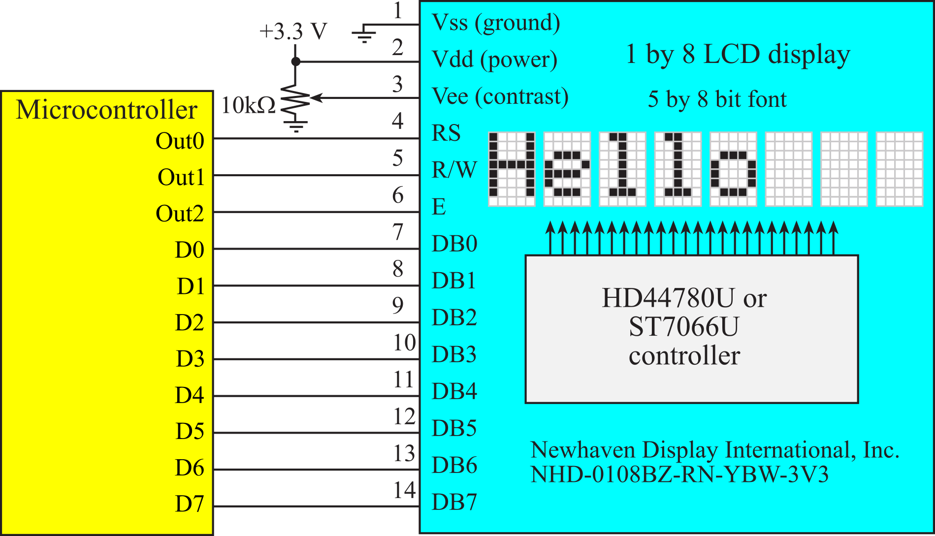
Figure 3.5.9. Character display interfaced to the microcontroller.
3.6. Buzzer
A more complex sound output will be presented in Chapter 5. In this section, we will interface a speaker to the microcontroller, outputting a square wave to generate a buzzing sound. MOSFETs are voltage-controlled switches. The difficulty with interfacing most MOSFETs to a microcontroller is the large gate voltage needed to activate some MOSFETs. Figure 3.5.1 shows two N-channel and one P-channel interfaces. We will model inductive loads like speakers, motors, solenoids, and electromagnetic relays as the series combination of resistance, inductance and emf voltage. The resistance arises from the long copper wire, the inductance arises from the fact the wire is coiled, and the emf is a bidirectional coupling between electrical power and mechanical power. We will learn more about this model when interfacing motors in Section 8.3. Binary Actuators. The voltage across an inductor is
V = L dI/dt
We must either limit dI/dt or use a snubber diode like the 1N914 to remove the L*dI/dt.
Observation: When we use a transistor to turn current on and off, the dI/dt from on to off will be much higher than the dI/dt from off to on.
If we wish to create a 2 kHz buzzing sound, we implement a 4 kHz periodic interrupt and toggle the output pin in the ISR.
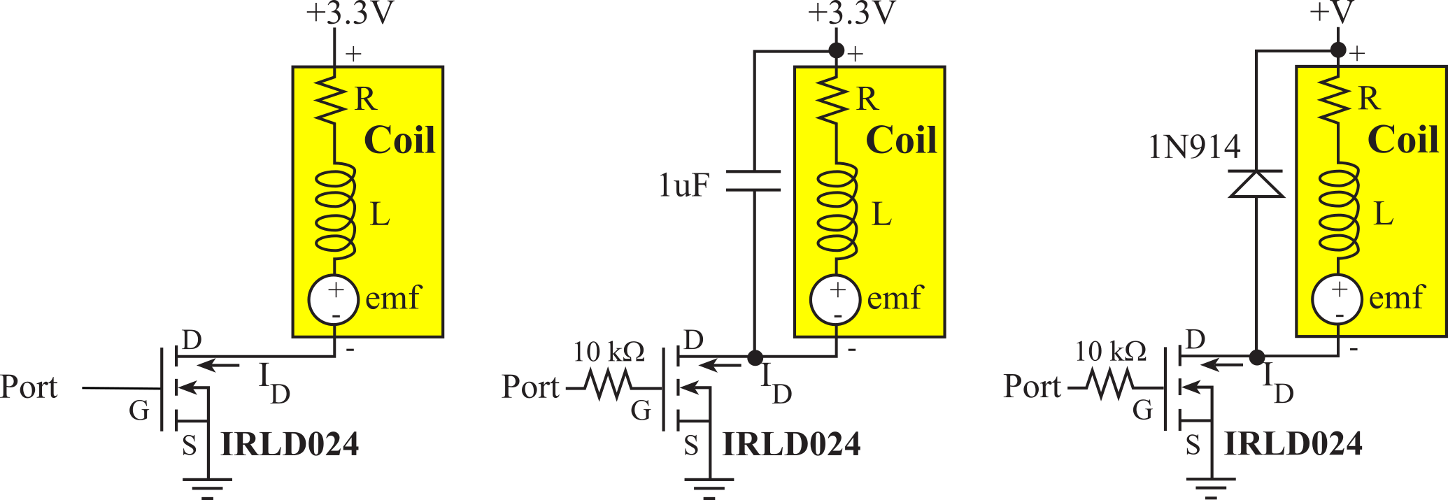
Figure 3.6.1. MOSFET interfaces to EM relay, solenoid, DC motor or speaker. IRLD024 data sheet.
The IRLD024 can be controlled directly from a port pin because the IRLD024 will activate with a gate voltage VGS at 2V or larger. The 10k resistor between the port and the IRLD024 gate does not affect the on or off voltages at the drain, but the 10k resistor does decrease dI/dt. Figure 3.6.2 shows the voltage at the IRLD024 drain pin without the diode or the 10k resistor. Notice that L dI/dt reaches 25V when the current goes from on to off.
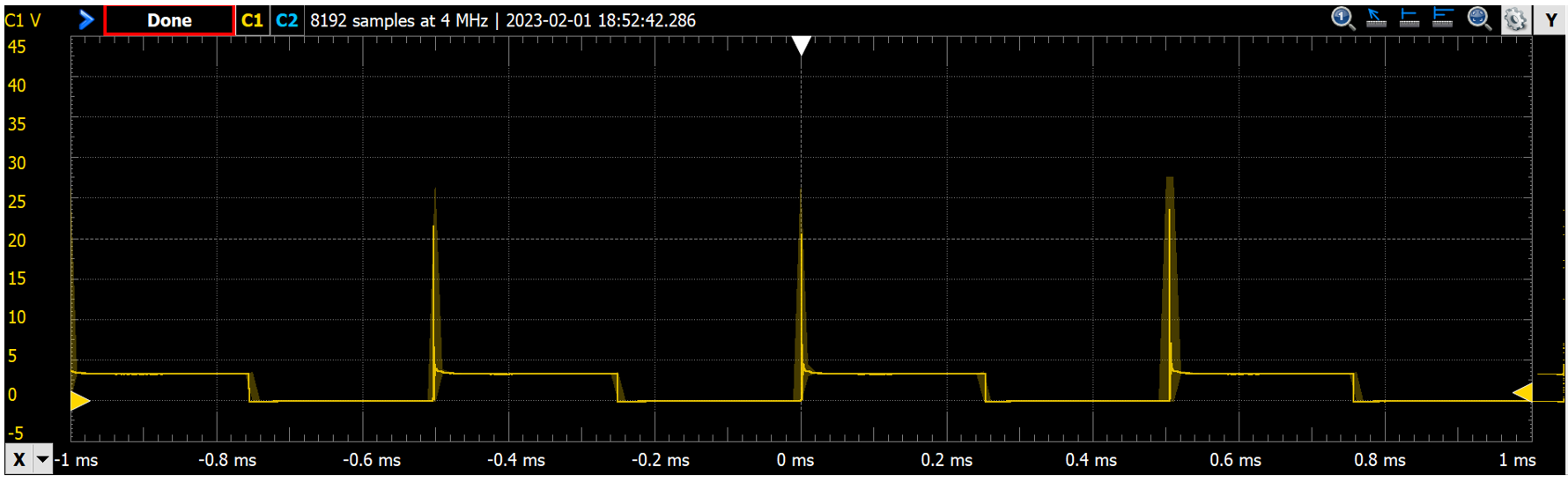
Figure 3.6.2. Scope trace of the voltage on the speaker, with a 32-ohm speaker, no resistor between pin and gate, no 1N914, and a IRLD024 MOSFET.
Figure 3.6.3 presents simplified Id versus VDS curves for four different MOSFETs. The curves have a linear range, where Id increases with Vds. The curve will then have a saturated range where the current cannot be increased. The transition between linear and saturation depends on the gate voltage VGS. The first step in choosing a MOSFET is selecting the VGS to activate the voltage-controlled switch. If possible, we would like to interface a microcontroller output pin directly to the gate. In MOSFETs A and B, the 3.3V VOH of the digital output is not large enough to activate the MOSFET. Later in Section 6.3.2 we will interface MOSFETs like A and B, but in this section, we will consider MOSFETs C and D, because both will fully activate with a VGS of 3.3V. The second step in choosing a MOSFET is selecting one with ID large enough to operate the load. MOSFET C will have a VDS less the 0.1V for ID less than 2A. In contrast, MOSFET D can only operate with drain current less than 1 A.
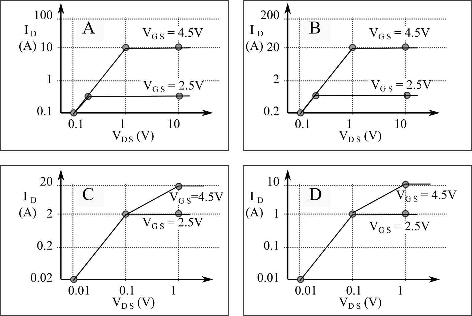
Figure 3.6.3. Simplified MOSFET curves.
Observation: The 1N914 diode removes the back EMF generated by the inductance of the load when current is removed. V = LdI/dt, which could be 100's of volts for large inductive loads like motors.
3.7. Scheming and Teaming
3.7.1. Design steps
This section lists questions we must answer when starting a new design.
What problem are we trying to solve? One effective way to find problems is to immerse ourselves in the real world. You could travel, avoiding the tourist sites. You could learn a new language. You could learn a new skill. You could spend a day following an expert: doctor, truck driver, carpenter, farmer, etc. You must have domain experts on your team to create systems that truly transform the way things are done. You must learn the language/culture of the domain. These domain experts are then invited into all aspects of the design process.
How is the design to be tested? How is it to be evaluated? We begin every design at the end. We must understand what the system is to do, then we can plan how to test and evaluate it.
What are your inputs? We start with, "what the system needs to know?" We then select input devices to collect that information.
What are your outputs? We ask, "what does the system need to do?" We then select output devices to perform those operations.
How will the user interact with the system? We consider switches, LEDs, sound, touch screen displays, battery charging, and graphical displays.
How might the system fail? We identify risks and include a backup plan.
In summary, we write a requirements document, see Section 1.4.1. In this document we list constraints, requirements, timetable, budget, available parts, user interface, enclosure size/weight, power budget, and wireless capabilities. When writing technical documents use these three words very carefully.
Must: The verb 'must' denotes a mandatory requirement, legal, regulatory, or standard, that is imposed by an outside agency. Failure to achieve this requirement precludes commercialization of the system.
Shall: The verb 'shall' denotes mandatory requirements specified by the company. Failure to achieve this requirement may preclude commercialization of the system.
Should: The verb 'should' denotes additional requirements that will be addressed by the development program if development time, development cost, and other constraints of the program allow.
There are two approaches to design. The top-down approach starts with a general overview, like an outline of a paper, and builds refinement into subsequent layers. A top-down designer was once quoted as saying,
"Write no software until every detail is specified"
Top-down provides a better global approach to the problem. Managers like top-down because it gives them tighter control over their workers. The top-down approach works well when an existing operational system is being upgraded or rewritten.
On the other hand, the bottom-up approach starts with the smallest detail, builds up the system "one brick at a time." The bottom-up approach provides a realistic appreciation of the problem because we often cannot appreciate the difficulty or the simplicity of a problem until we have tried it. It allows engineers to start immediately building and gives engineers more input into the design. For example, a low-level engineers may be able to point out features that are not possible and suggest other features that are even better. Some projects are flawed from their conception. With bottom-up design, the obvious flaws surface early in the development cycle.
I believe bottom-up is better when designing a complex system and specifications are open-ended. On the other hand, top-down is better when you have a very clear understanding of the problem specifications and the constraints of your computer system. One of the best systems I have ever been part of was actually designed twice. The first design was built bottom up and served only to provide a clear understanding of the problem, clarification of the features needed, and the limitations of the hardware and software. We literally threw all the source code and circuit designs, and we reengineered the system in a top-down manner.
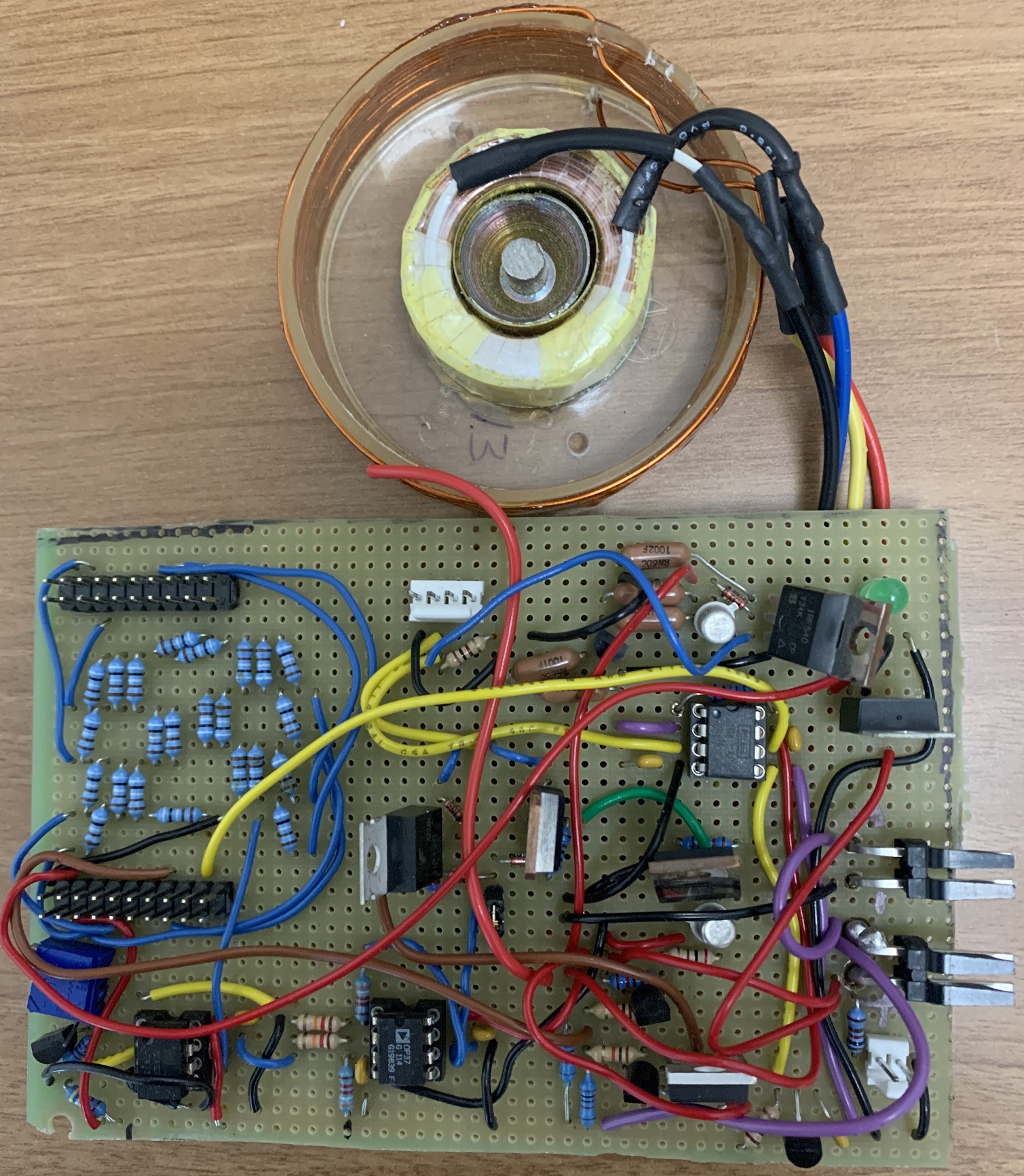
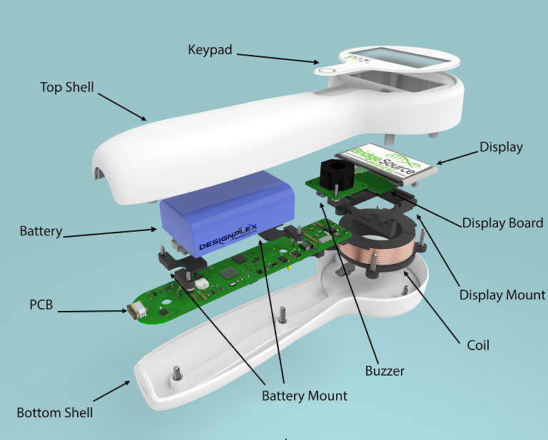
Figure 3.7.1. Medical Device Identifier: original design and final device ready for FDA approval by DesignPlex Biomedical and Bridgesource Medical. https://www.bridgesourcemedical.com/diagnostics
Arthur C. Clarke's Third Law: Any sufficiently advanced technology is indistinguishable from magic.
J. Porter Clark's Law: Sufficiently advanced incompetence is indistinguishable from malice.
: What is the importance of a domain expert in the initial stages of a design?
3.7.2. Modular Programming
The key to completing any complex task is to break it down into manageable subtasks. Modular programming or functional abstraction is a style of software development that divides the software problem into distinct and independent modules. The parts are as small as possible, yet relatively independent. Complex systems designed in a modular fashion are easier to debug because each module can be tested separately. Industry experts estimate that 50 to 90% of software cost is spent in maintenance. All five aspects of software maintenance are simplified by organizing the software system into modules.
• Correcting mistakes
• Adding new features
• Optimizing execution speed
• Reducing program size
• Porting to new computers or operating systems
•
Reconfiguring the software to solve similar related programs
Observation: Modularity is improved by maximizing the number of modules, minimizing coupling, and maximizing cohesion.
Modular programming is separating "what the function does" from "how the function works". We can think of it as the three I's:
• Interface: specifying the function names, input parameters, and output parameters
• Implementation: the code that makes the functions work
• Invocation: calling the functions
We place function prototypes (interfaces) in the header file. In the header file, we describe "what it does." We place the function definitions (implementations) in the code file. In the code file, we describe "how it works." There is a third file, called testmain, into which we place example usage of the functions (invocations). In the testmain.c file, we also describe "how it was tested."
A module is a collection of functions that perform a well-defined set of tasks. The collection of serial port I/O functions can be considered one module. A collection of 32‑bit math operations is another example of a module. Modular programming involves both the definition of modules and the connection scheme by which the modules are connected to form the software system (call graph). While the module may be called from many locations throughout the system, there should be well-defined interfaces into the module, specified by the prototypes to public functions listed in the header file.
The overall goal of modular programming is to enhance clarity. The smaller the task, the easier it will be to understand. Coupling is defined as the influence one module's behavior has on another module. To make modules more independent we strive to minimize coupling.
Obvious and appropriate examples of coupling are the input/output parameters explicitly passed from one module to another. On the other hand, information stored in shared global variables can be quite difficult to track. Like global variables, shared access to I/O ports can also introduce unnecessary complexity. Global variables and shared I/O cause coupling between modules that complicate the debugging process because now the modules may not be able to be separately tested. On the other hand, we must use global variables to pass information into and out of an interrupt service routine, and from one call to an interrupt service routine to the next call. Consequently, we create private permanently-allocated variables (declared as static) in one module so interactions can be managed. Similarly, we divide I/O into logical groups (e.g., ADC, Timer0, UART1) and place all access to each I/O group in a separate module. If we need to pass data from one module to another, we use a well-defined interface technique like a mailbox or first-in-first-out (FIFO) queue.
Assign a logically complete task to each module. The module is logically complete when it can be separated from the rest of the system and placed into another application. The interfaces are extremely important (the header file). The interfaces determine the policies of our modules. In other words, the interfaces define the operations of our software system. The interfaces also represent the coupling between modules. In general, we wish to minimize the amount of information passing between the modules yet maximize the number of modules. Of the following three objectives when dividing a software project into subtasks, it is only the first one that matters.
• Make the software project easier to understand
• Increase the number of modules
• Decrease the interdependency (minimize coupling)
We can develop and connect modules in a hierarchical manner. Construct new
modules by combining existing modules. In a hierarchical system the modules are
organized into a tree-structured call graph. In the call graph, an arrow points
from the calling routine to the module it calls. The I/O ports are organized
into groups (e.g., all the serial port I/O registers are in one group). The
call graph allows us to see the organization of the project. To make simpler
call graphs on large projects we can combine multiple related functions into a
single module. The main program is at the top and the I/O ports are at the
bottom. In a hierarchical system the modules are organized both in a horizontal
fashion (grouped together by function) and in a vertical fashion (overall
policies decisions at the top and implementation details at the bottom). Since
one of the advantages of breaking a large software project into subtasks is
concurrent development, it makes sense to consider concurrency when dividing
the tasks. In other words, the modules should be partitioned in such a way that
multiple programmers can develop the subtasks as independently as possible. On
the other hand, careful and constant supervision is required as modules are
connected and tested.
Observation: If module A calls module B, and module B calls module A, then you have created a special situation that must account for these mutual calls.
From a formal perspective, I/O devices are considered as global. This is because I/O devices reside permanently at fixed addresses. From a syntactic viewpoint any module has access to any I/O device. To reduce the complexity of the system we will restrict the number of modules that actually do access the I/O device. It will be important to clarify which modules have access to I/O devices and when they are allowed to access it. When more than one module accesses an I/O device, then it is important to develop ways to arbitrate (which module goes first if two or more want to access simultaneously) or synchronize (make a second module wait until the first is finished.)
Information hiding is like minimizing coupling. It is better to separate the mechanisms of software from its policies. We should separate what the function does (the relationship between its inputs and outputs) from how it does it. It is good to hide certain inner workings of a module, and simply interface with the other modules through the well-defined input/output parameters. For example, we could implement a FIFO by maintaining the current number of elements in a global variable, Count. A good module will hide how Count is implemented from its users. If the user wants to know how many elements are in the FIFO, it calls a TxFifo_Size() routine that returns the value of Count. A badly written module will not hide Count from its users. The user simply accesses the global variable Count. If we update the FIFO routines, making them faster or better, we might have to update all the programs that access Count too. The object-oriented programming environments provide well-defined mechanisms to support information hiding. This separation of policies from mechanisms can be seen also in layered software.
The Keep It Simple Stupid approach tries to generalize the problem so that it fits an abstract model. Unfortunately, the person who defines the software specifications may not understand the implications and alternatives. Sometimes we can restate the problem to allow for a simpler (and possibly more powerful) solution. As a software developer, we always ask ourselves these questions:
"How important is this feature?"
"What alternative ways could this system be structured?"
"How can I
redefine the problem to make it simpler?"
We can classify the coupling between modules as highly coupled, loosely coupled, or uncoupled. A highly-coupled system is not desirable, because there is a great deal of interdependence between modules. A loosely-coupled system is optimal, because there is some dependence but interconnections are weak. An uncoupled system, one with no interconnections at all, is typically inappropriate in an embedded system, because all components should be acting towards a common objective. There are three ways in which modules can be coupled. The natural way in which modules are coupled is where one module calls or invokes a function in a second module. This type of coupling, called invocation coupling, can be visualized with a call graph, quantified as the number of calls per fixed time. A second way modules can be coupled is by data transfer. If information flows from one module to another, we classify this as bandwidth coupling. Bandwidth, which is the information transfer rate, is a quantitative measure of coupling. Bandwidth coupling can be visualized with a data flow graph. The third type of coupling, called control coupling, occurs when actions in one module affect the control path within another module. For example, if Module A sets a global flag and Module B uses the global flag to decide its execution path. Control coupling is hard to visualize and hard to debug. Therefore, it is a poor design to have module interactions with control coupling.
Another way to categorize coupling is to examine how information is passed or shared between modules. We will list the mechanisms from poor to excellent. It is extremely poor design to use globals and allow Module A directly modify data or flags within Module B. Similarly poor design is to organize important data into a common shared global space and allow modules to read and write these data. It is ok to allow Module A to call Module B and pass it a control flag. This control flag will in turn affect the execution within Module B. It is good design to have one module pass data to another module. Data can be structured or unstructured (called primitive). Examples of structured data include
time (hour, minutes, seconds)
stamped (data, time of recording)
images (bmp, jpg, png)
vector drawing (svg)
sounds (wav, mp3)
Coupling defines inter-module connections. On the other hand, intra-module connections are also important. We need a way to describe how various components within a module interact with each other. For example, consider a system with 100 functions. How should one divide these functions into modules?
Cohesion is the degree of interrelatedness of internal parts within the module. In general, we wish to maximize cohesion. A cohesive module has all components of the module are directed towards and essential for the same task. It is also important to analyze how components are related as we design modules. Coincidental cohesion occurs when components of the module are unrelated, resulting in poor design. Examples of coincidental cohesion would be a collection of frequently used routines, a collection of routines written by a single programmer, or a collection of routines written during a certain time interval. It is a poor design to have modules with coincidental cohesion.
Logical cohesion is a grouping of components into a single module because they perform similar functions. An example of logical cohesion is a collection of serial output, LCD output, and network output routines into one module because all routines perform output. Organizing modules in this fashion is also poor design and results in modules that are hard to reuse.
Temporal cohesion combines components if they are connected in time sequence. If we are baking bread, we activate the yeast in warm water in one bowl, and then we combine the flour, sugar, and spices in another bowl. These two steps are connected only in the sense that we first do one, and then we do another when making bread. If we were making cookies, we would need flour, sugar, and spices but not the yeast. Temporal cohesion is poor design because when we want to mix and match existing modules to create new designs, we expect the sequence of module execution to change.
Another poor design, called procedural cohesion, groups functions together in order to ensure mandatory ordering. For example, an embedded system might have an input port, an output port, and a timer module. To work properly, all three must be initialized. It would be hard to reuse code if we placed all three initialization routines into one module.
We next present appropriate reasons to group components into one module. Communicational cohesion exists when components operate on the same data. An example of communicational cohesion would be a collection of routines that filter and extract features from the data.
Sequential cohesion occurs when components are grouped into one module, because the output from one component is the input to another component. Sequential cohesion is a natural consequence of minimizing bandwidth between modules. An example of sequential cohesion is a fuzzy logic controller. This controller has five stages: crisp input, fuzzification, rules, defuzzification, and crisp output. The output of each stage is the input to the next stage. The input bandwidth to the controller and the output bandwidth from the controller can be quite low, but the amount of information transferred between stages can be thousands of times larger. Executing machine learning models has this same sequential cohesion, because the output of one stage will be the input to the next.
The best kind of cohesion is functional cohesion, where all components combine to implement a single subsystem, and each component has a necessary contribution to the objective. I/O device drivers, which are a collection of routines for a single I/O device, exhibit functional cohesion.
Another way to classify good and bad modularity is to observe fan in and fan out behavior. In a data flow graph, the tail of an arrow defines a data output, and the head of an arrow defines a data input. The fan in of a module is the number of other modules that have direct control on that module. Fan in can be visualized by counting the number of arrowheads that terminate on the module in the data flow graph, shown previously in Figure 1.4.2. The fan out of a module is the number of other modules directly controlled by this module. Fan out can be visualized by counting the number of tails of arrows that originate on the module in the data flow graph. In general, a system with high fan out is poorly designed, because that one module may constitute a bottleneck or a critical safety path. In other words, the module with high fan out is probably doing too much, performing the tasks that should be distributed to other modules. High fan in is not necessarily a poor design, depending on the application.
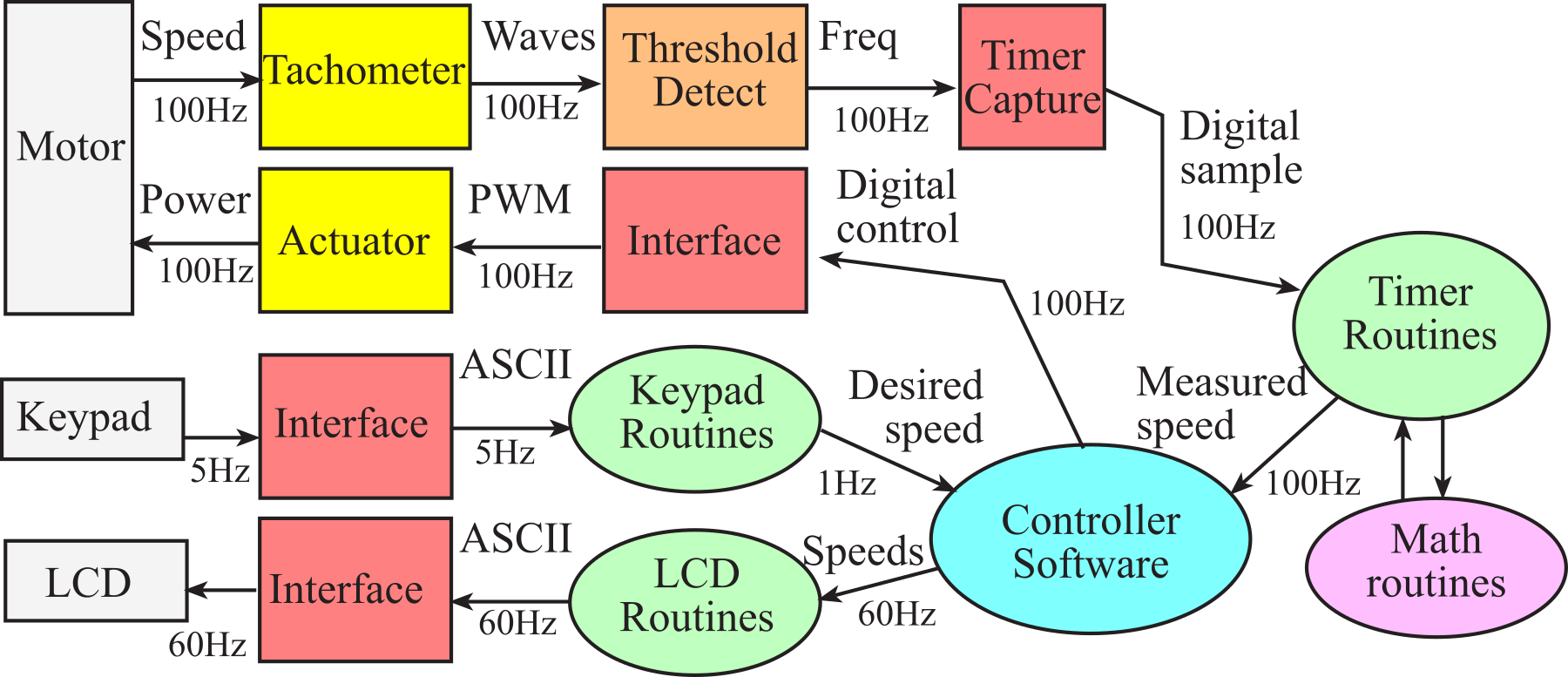
Figure 1.4.2. A data flow graph showing how signals pass through a motor controller.
: What is the fan in and fan out of the Controller Software in Figure 1.4.2?
3.7.3. Clients and Coworkers
Good engineers employ well-defined design processes when developing complex systems. When we work within a structured framework, it is easier to prove our system works (verification) and to modify our system in the future (maintenance). As our systems become more complex, it becomes increasingly important to employ well-defined design processes. In this chapter, a very detailed set of software development rules will be presented. At first, it may seem radical to force such a rigid structure to software. We might wonder if creativity will be sacrificed in the process. True creativity is more about effective solutions to important problems and not about being sloppy and inconsistent. Because maintenance is a critical task, the time spent organizing, documenting, and testing during the initial development stages will reap huge dividends throughout the life of the project.
Observation: The easiest way to debug is to write software without any bugs.
We define clients as people who will use our software. Sometimes, the client is the end-user who uses the embedded system. Other times, we develop hardware/software components that plug into a larger system. In this case, the client develops hardware/software that will use our components. We define coworkers as engineers who will maintain our system. We must make it easy for a coworker to debug, use, and extend our system.
: Of the three I's which two are meant for the clients?
Developing quality systems has a lot to do with attitude. We should be embarrassed to ask our coworkers to make changes to our poorly written software or sloppy hardware designs. Since so much of a system's life involves maintenance, we should create components that are easy to change. In other words, we should expect each piece of our designs will be read by another engineer in the future, whose job it will be to make changes to our design. We might be tempted to quit a project once the system is running, but this short time we might save by not organizing, documenting, and testing will be lost many times over in the future when it is time to update the system.
Observation: Much of the engineering design that university professors require of their students is completely unrealistic. Professors give a lab assignment on day 1, expect the students to complete it with demo and report 7 days later, and then the professors grade it. Often, professors give passing grades for designs that only partially work. The design is then tossed in the trash never to be looked at again.
As project managers, we must reward good behavior and punish bad behavior. A company, to improve the quality of their software products, implemented the following policies.
"The employees in the customer relations department receive a bonus for every software bug that they can identify. These bugs are reported to the software developers, who in turn receive a bonus for every bug they fix."
: Why did the above policy fail horribly?
We should demand of ourselves that we deliver bug-free software to our clients. Again, we should be embarrassed when our clients report bugs in our code. We should be ashamed when other programmers find bugs in our code. There are five steps we can take to facilitate this important aspect of software design.
Test it now. When we find a bug, fix it immediately. The longer we put off fixing a mistake the more complicated the system becomes, making it harder to find. Remember that bugs do not go away automatically, but we can make the system so complex that the bugs will manifest themselves in a mysterious and obscure fashion. For the same reason, we should completely test each module individually, before combining them into a larger system. We should not add new features before we are convinced the existing features are bug-free. In this way, we start with a working system, add features, and then debug this system until it is working again.
This incremental approach makes it easier to track progress. It allows us to undo bad decisions, because we can always revert to a previous working system. Adding new features before the old ones are debugged is very risky. With this sloppy approach, we could easily reach the project deadline with 100% of the features implemented but have a system that doesn't run. In addition, once a bug is introduced, the longer we wait to remove it, the harder it will be to correct. This is particularly true when the bugs interact with each other. Conversely, with the incremental approach, when the project schedule slips, we can deliver a working system at the deadline that supports some of the features.
Maintenance Tip: Go from working system to working system.
Plan for testing. How to test should be considered at the beginning, middle, and end of a project. Testing should be included as part of the initial design. Our testing and the client's usage go hand in hand. How we test the software module will help the client understand the context and limitations of how our software is to be used. It often makes sense to explain the testing procedures to the client as an effort to communicate the features and limitations of the module. Furthermore, a clear understanding of how the client wishes to use our software is critical for both the software design and its testing. For example, after seeing how you tested the module, the client may respond, "That's nice, but what I really want it to do is ...". If this happens, it makes sense to rewrite the requirements document to reflect this new understanding of the client's expectation.
Maintenance Tip: It is better to have some parts of the system that run with 100% reliability than to have the entire system with bugs.
Get help. Use whatever features are available for organization and debugging. Pay attention to warnings, because they often point to misunderstandings about data or functions. Misunderstanding of assumptions can cause bugs when the software is upgraded or reused in a different context than originally conceived. Remember that computer time is a lot cheaper than programmer time. It is a mistake to debug an embedded system simply by observing its inputs and outputs. We need to use both software and hardware debugging tools to visualize internal parameters within the system.
Maintenance Tip: It is better to have a system that runs slowly than to have one that doesn't run at all.
Divide and conquer. In the early days of microcomputer systems, software size could be measured in hundreds of lines of source code or thousands of bytes of object code. These early systems, due to their small size, were inherently simple. The explosion of hardware technology (both in speed and size) has led to a similar increase in the size of software systems. The only hope for success in a large software system will be to break it into simple modules. In most cases, the complexity of the problem itself cannot be avoided. E.g., there is just no simple way to get to the moon. Nevertheless, a complex system can be created out of simple components. A real creative effort is required to orchestrate simple building blocks into larger modules, which themselves are grouped. We use our creativity to break a complex problem into simple components, rather than developing complex solutions to simple problems.
Observation: There are two ways of constructing a software design: one way is to make it so simple that there are obviously no deficiencies and the other way is make it so complicated that there are no obvious deficiencies. C.A.R. Hoare, "The Emperor's Old Clothes," CACM Feb. 1981.
Avoid inappropriate I/O. One of the biggest mistakes beginning programmers make is the inappropriate usage of I/O calls (e.g., screen output and keyboard input). An explanation for their foolish behavior is that they haven't had the experience yet of trying to reuse software they have written for one project in another project. Software portability is diminished when it is littered with user input/output. To reuse software with user I/O in another situation, you will almost certainly have to remove the input/output statements. In general, we avoid interactive I/O at the lowest levels of the hierarchy, rather return data and flags and let the higher-level program do the interactive I/O. Often we add keyboard input and screen output calls when testing our software. It is important to remove the I/O that not directly necessary as part of the module function. This allows you to reuse these functions in situations where screen output is not available or appropriate. Obviously, screen output is allowed if that is the purpose of the routine.
Common Error: Performing unnecessary I/O in a subroutine makes it harder to reuse at a later time.
3.7.4. Software Performance Metrics
Software development is like other engineering tasks. We can choose to follow well-defined procedures during the development and evaluation phases, or we can meander in a haphazard way and produce code that is hard to test and harder to change. The goal of the system is to satisfy the stated objectives such as accuracy, stability, and input/output relationships. Nevertheless, it is appropriate to separately evaluate the individual components of the system. Therefore, in this section, we will evaluate the quality of our software. There are two categories of performance criteria with which we evaluate the "goodness" of our software. Quantitative criteria include dynamic efficiency (speed of execution), static efficiency (ROM and RAM program size), and accuracy of the results. Qualitative criteria center on ease of software maintenance. Another qualitative way to evaluate software is ease of understanding. If your software is easy to understand then it will be:
Easy to debug, including both finding and fixing mistakes
Easy to verify, meaning we can prove it is correct
Easy to maintain, meaning we can add new features
Common error: Programmers who sacrifice clarity in favor of execution speed often develop software that runs fast but is error-prone and difficult to change.
Golden Rule of Software Development: Write software for others as you wish they would write for you.
To evaluate our software quality, we need performance measures. The simplest approaches to this issue are quantitative measurements. Dynamic efficiency is a measure of how fast the program executes. It is measured in seconds or processor bus cycles. Because of the complexity of the Cortex-M, it will be hard to estimate execution speed by observing the assembly language generated by the compiler. Rather, we will employ methods to experimentally measure execution speed (see Section 1.11.4 Performance Debugging and see 1.11.5 Profiling). Static efficiency is the number of memory bytes required. Since most embedded computer systems have both RAM and ROM, we specify memory requirement in global variables, stack space, fixed constants, and program object code. The global variables plus maximum stack size must fit into the available RAM. Similarly, the fixed constants plus program size must fit into the available ROM. We can judge our software system according to whether it satisfies given constraints, like software development costs, memory available, and timetable. Many of the system specifications are quantitative, and hence the extent to which the system meets specifications is an appropriate measure of quality.
Qualitative performance measurements include those parameters to which we cannot assign a direct numerical value. Often in life the most important questions are the easiest to ask, but the hardest to answer. Such is the case with software quality. So therefore, we ask the following qualitative questions. Can we prove our software works? Is our software easy to understand? Is our software easy to change? Since there is no single approach to writing quality software, I can only hope to present some techniques that you may wish to integrate into your own software style. In fact, we will devote most of this chapter to the important issue of developing quality designs. We will study self-documented code, abstraction, modularity, and layered software. These parameters indeed have a profound effect on the bottom-line financial success of our projects. Although quite real, because there is often not an immediate and direct relationship between software quality and profit, we may be tempted to dismiss its importance.
Observation: Most people get better with practice. So, if you wish to become a better programmer, I suggest you write great quantities of software.
: A common saying is it takes 10,000 hours of practice to reach expert status. Assume you can write a rate of 100 lines of good code per hour. How many lines of code will it take for you to become an expert? Don't be discouraged, the path to excellence is taken one step at a time.
To get a benchmark on how good a programmer you are, I challenge you to do two tests. In the first test, find a major piece of software that you have written over 12 months ago, and then see if you can still understand it enough to make minor changes in its behavior. The second test is to exchange with a peer a major piece of software that you have both recently written (but not written together), then in the same manner, if you can make minor changes to each other's software.
Observation: You can tell if you are a good programmer if 1) you can understand your own code 12 months later, and 2) others can make changes to your code.
3.7.5. Enhancing Team Skills
A team is a small number of people with complementary skills who are committed to a common purpose, performance goals, and approach for which they are mutually accountable.
When we form teams, we expect the following behaviors, which could involve a signed contract pledging to:
• Be respectful of yourself and others
• Listen attentively without judging and without criticism
• Remove your ego from the discussions
• Answer communication quickly, even if you need to say "I'll get back to you later"
• Give constructive feedback
• Agree on a time and place to meet
• Team members form relationships, caring for each other
• Put a time limit on meetings, start on time, end on time
Effective team checklist
• Define and understand the common goal for the project
• Make a list of tasks to be completed
• Be dedicated to the goal with unified effort
• Problems and changes are anticipated and accepted
• Assign responsibility for all tasks and distribute them appropriately
• Develop a timeline and stick to it, but allow for slippage
• Develop and post a Gantt chart for the plan
• Document key decisions and actions from all team meetings
• Send reminders when deadlines approach
• Send confirmation when tasks are completed
• Collectively review the project output for quality
Skills to manage conflict
• Acknowledge that the conflict exists and stay focused on the goal
• Gain common ground
o Seek to understand all angles: Let each person state his or her view briefly
o Have neutral team members reflect on areas of agreement or disagreement
o Explore areas of disagreement regarding specific issues
o Have opponents suggest modifications to their points of view as well as others
o If consensus is blocked, ask opponents if they can accept the team's decision
• Attack the issue, not each other
• Develop an action plan.
References
1. Katzenbach, J.R. & Smith, D.K. (2015). The Wisdom of Teams: Creating the High-performance Organization. Boston: Harvard Business School.
2. Breslow, L. Teaching Teamwork Skills, Part 2. Teach Talk,
3. High Performance Team Essential Elements. Penn State University
4. https://www.tempo.io/blog/signs-strong-teamwork
3.8. Software Style Guidelines
One of the wonderful benefits of being project leader is the establishment of software style guidelines. These guidelines are not necessary for the program to compile or to run. Rather the intent of the rules is to make the software easier to understand, easier to debug, and easier to change. Just like beginning an exercise program, these rules may be hard to follow at first, but the discipline will pay dividends in the future.
Observation: There are many style guidelines from which you could select. It is not important to follow our guidelines, but rather it is important to follow some guidelines.
3.8.1. Variables
Variables are an important component of software design, and there are many factors to consider when creating variables. Some of the obvious considerations are the allocation, size, and format of the data. However, an important factor involving modular software is scope. The scope of a variable defines which software modules can access the data. Variables with a restricted access are classified as private, and variables shared between multiple modules are public. We can restrict the scope to a single file, a single function, or even a single program block within a matching pair of braces, {}. In general, the more we limit the scope of our variables the easier it is to design (because the modules are smaller and simpler), to change (because code can be reused), and to verify (because interactions between modules are well-defined). However, since modules are not completely independent, we need a mechanism to transfer information from one to another. The allocation of a variable specifies where or how it exists. Because their contents are allowed to change, all variables must be allocated in registers or in RAM, but not in ROM. Constants can and should be allocated in ROM. Global variables contain information that is permanent and are usually assigned a fixed location in RAM. Global variables have public scope, in other words can be accessed by any software. Local variables contain temporary information and are stored in a register or allocated on the stack. Static variables have permanent allocation but restricted scope. Static variables can have scope restricted to one file, to one function or just within one brace.
A local variable has temporary allocation because we create local variables on the stack or in registers. Because the stack and registers are unique to each function, this information cannot be shared with other software modules. Therefore, under most situations, we can further classify these variables as private. Local variables are allocated, used, and then deallocated, in this specific order. For speed reasons, we wish to assign local variables to a register. When we assign local variable to a register, we can do so in a formal manner. There will be a certain line in the assembly software at which the register begins to contain the variable (allocation), followed by lines where the register contains the information (access or usage), and a certain line in the software after which the register no longer contains the information (deallocation). In C, we define local variables after an opening brace.
void MyFunction(void){ uint16_t i; // i is a local
for(i = 0; i < 10; i++){ uint32_t j; // j is a local
j = i+100;
UART_OutUDec(j);
}
}
The information stored in a local variable is not permanent. This means if we store a value into a local variable during one execution of the module, the next time that module is executed the previous value is not available. Examples include loop counters and temporary sums. We use a local variable to store data that are temporary in nature. With a local variable only the program that created the local variable can access it. We can implement a local variable using the stack or registers. Some reasons why we choose local variables over global variables:
• Dynamic allocation/release allows for reuse of RAM
• Limited scope of access (making it private) provides for data protection
• Since an interrupt will save registers and create its own stack frame, it works correctly if called from multiple concurrent threads (reentrant)
• Since absolute addressing is not used, the code is relocatable
A global variable is allocated permanently in RAM and fixed location in RAM. A public global variable contains information that is shared by more than one program module. We must use parmanently allocated variables to pass data between the main program (i.e., foreground thread) and an ISR (i.e., background thread). Defining the variable as static, private to the file, reduces the scope making it easier to debug. Global and static variables are allocated at compile time and never deallocated. The information they store is permanent. Examples include time of day, date, calibration tables, user name, temperature, FIFO queues, and message boards. When dealing with complex data structures, pointers to the data structures are shared. In general, it is a poor design practice to employ public global variables. On the other hand, static variables are necessary to store information that is permanent in nature. In C, we define global variables outside of the function.
int32_t Count=0; // Count is a global variable
void MyFunction(void){
Count++; // number of times function was called
}
: How do you create a local variable in C?
Sometimes we store temporary information in global variables out of laziness. This practice is to be discouraged because it wastes memory and may cause the module to work incorrectly if called from multiple concurrent threads (non-reentrant). Non-reentrant programs can produce very sneaky bugs, since they might only crash in rare situations when the same code called from different threads when the first thread is in a particular critical section. Such a bug is difficult to reproduce and diagnose. In general, it is good design to limit the scope of a variable as much as possible.
: How do you create a global variable in C?
In C, a static local has permanent allocation, which means it maintains its value from one call to the next. It is still local in scope, meaning it is only accessible from within the function. I.e., modifying a local variable with static changes its allocation (it is now permanent), but doesn't change its scope (it is still private). In the following example, count contains the number of times MyFunction is called. The initialization of a static local occurs just once, during startup.
void MyFunction(void){
static int32_t count=0;
count++; // number of times function was called
}
In C, we create a private global variable using the static modifier. Adding static to an otherwise global variable does not change its allocation (it is still permanent), but does reduce its scope. Regular globals can be accessed from any function in the system (public), whereas a static variable can only be accessed by functions within the same file. Static globals are private to that particular file. Functions can be static also, meaning they can be called only from other functions in the file. E.g.,
static int16_t myPrivateGlobalVariable; // accessed in this file only
void static MyPrivateFunction(void){ // accessed in this file only
// can access myPrivateGlobalVariable
}
In C, a const global is read-only. It is allocated in the ROM. Constants, of course, must be initialized at compile time. E.g.,
const int16_t Slope=21;
const uint8_t SinTable[8]={0,50,98,142,180,212,236,250};
: How does the static modifier affect locals, globals, and functions in C?
: How does the const modifier affect a global variable in C?
: How does the const modifier affect a function parameter in in C?
If you leave off the const modifier in the SinTable example, the table will be allocated twice, once in ROM containing the initial values, and once in RAM containing data to be used at run time. Upon startup, the system copies the ROM-version into the RAM-version.
Maintenance Tip: It is good practice to specify the units of a variable (e.g., volts, cm etc.).
Maintenance Tip: It is good practice to reduce the scope as much as possible.
In summary, there are three types of variables:
Globals (public scope, permanent allocation),
Statics (private scope, permanent allocation), and
Locals (private scope, temporary allocation).
3.8.2. Organization of a code file
One of the recurring themes of this software style section is consistency. Maintaining a consistent style will help us locate and understand the different components of our software, as well as prevent us from forgetting to include a component or worse, including it twice.
The following regions should occur in this order in every code file (e.g., file.c).
Opening comments. The first line of every file should contain the file name. Remember that these opening comments will be duplicated in the corresponding header file (e.g., file.h) and are intended to be read by the client, the one who will use these programs. If major portions of this software are copied from copyrighted sources, then we must satisfy the copyright requirements of those sources. The rest of the opening comments should include
• The overall purpose of the software module
• The names of the programmers
• The creation (optional) and last update dates
• The hardware/software configuration required to use the module
•
Copyright information
Including .h files. Next, we will place the #include statements that add the necessary header files. Normally the order doesn't matter, so we will list the include files in a hierarchical fashion starting with the lowest level and ending at the highest high. If the order of these statements is important, then write a comment describing both what the proper order is and why the order is important. Putting them together at the top will help us draw a call graph, which will show us how our modules are connected. In particular, if we consider each code file to be a separate module, then the list of #include statements specify which other modules can be called from this module. Of course, one header file is allowed to include other header files. However, we should avoid having one header file include other header files. This restriction makes the organizational structure of the software system easier to observe. Be careful to include only those files that are absolutely necessary. Adding unnecessary include statements will make our system seem more complex than it is.
Including .c files. You should not include other code files, rather code files are listed in the project settings. Including code files confuses the overall structure of the software system.
Observation: Looking at the project window and the #include statements, one can draw the system call graph.
#define statements. Next, we should place the #define macros. These macros can define operations or constants. Since these definitions are located in the code file (e.g., file.c), they will be private. This means they are available within this file only. If the client does not need to use or change the macro operation or constant, then it should be made private by placing it here in the code file. Conversely, if we wish to create public macros, then we place them in the header file for this module.
struct union enum statements. After the define statements, we should create the necessary data structures using struct union and enum. Again, since these definitions are located in the code file (e.g., file.c), they will be private. If they need to be public, we place them in the header file.
Global variables, static variables, and constants. After the structure definitions, we should include the globals, statics, and constants. There are two aspects of data that are important. First, we can specify where the data is allocated. If it is a variable that needs to exist permanently, we will place it in RAM as a global or static. If it is a constant that needs to exist permanently, we will place it in ROM using const. If the data is needed temporarily, we can define it as a local. The compiler will allocate locals in registers or on the stack in whichever way is most efficient.
int32_t PublicGlobal; // accessible by any module
static int32_t PrivateStatic; // accessible in this file only
const int32_t Constant=1234567; // in ROM
void function(void){
static int32_t veryPrivateStatic; // accessible by this function only
int32_t privateLocal; // accessible by this function only
}
A global variable has permanent allocation and public scope. In the above examples, PublicGlobal PrivateGlobal and veryPrivateGlobal are global. Constant will be defined in ROM, and cannot be changed. We define a local variable as one with temporary allocation. The variable privateLocal is local and may exist on the stack or in a register.
The second aspect of the data is its scope. Scope specifies which software can access the data. Public variables can be accessed by any software. Private variables have restricted scope, which can be limited to the one file, the one function, or even to one {} program block. In general, we wish to minimize the scope of our data. Minimizing scope reduces complexity and simplifies testing. If we specify the global with static, then it will be private and can only be accessed by programs in this file. If we do not specify the global with static then it will be public, and it can be accessed any program. For example, the PublicGlobal variable can be defined in other files using extern and the linker will resolve the reference. However, the PrivateGlobal cannot be accessed from software outside of the one file in which this variable is defined. Again, we classify PrivateGlobal as private because its scope is restricted. We put all the globals together before any function definitions to symbolize the fact that any function in this file has access to these globals. If we have a permanent variable that is only accessed by one function, then it should be defined inside the function with static. For example, the variable veryPrivateGlobal is permanently allocated in RAM, but can only be accessed by the function.
Maintenance Tip: Reduce complexity in our system by restricting direct access to our data. E.g., make global variables static if possible.
Prototypes of private functions. After the globals, we should add any necessary prototypes. Just like global variables, we can restrict access to private functions by defining them as static. Prototypes for the public functions will be included in the corresponding header file. In general, we will arrange the code implementations in a top-down fashion. Although not necessary, we will include the parameter names with the prototypes. Descriptive parameter names will help document the usage of the function. For example, which of the following prototypes is easier to understand?
static void plot(int16_t, int16_t);
static void plot(int16_t time, int16_t pressure);
Maintenance Tip: Reduce complexity in our system by restricting the software that can call a function E.g., make functions static if possible.
Implementations of the functions. The heart of the implementation file will be, of course, the implementations. Again, private functions should be defined as static. The functions should be sequenced in a logical manner. The most typical sequence is top-down, meaning we begin with the highest level and finish with the lowest level. Another appropriate sequence mirrors the manner in which the functions will be used. For example, start with the initialization functions, followed by the operations, and end with the shutdown functions. For example:
Open
Input
Output
Close
Including .c files. If the compiler does not support projects, then we would end the file with #include statements that add the necessary code files. Since most compilers support projects, we should use its organizational features and avoid including code files. The project simplifies the management of large software systems by providing organizational structure to the software system. Again, if we use projects, then including code files will be unnecessary, and hence should be avoided.
Employ run-time testing. If our compiler supports assert() functions, use them liberally. Place assertions at the beginning of functions to test the validity of the input parameters. Place assertions after calculations to test the validity of the results. Place assertions inside loops to verify indices and pointers are valid. There is a secondary benefit to assertions; they provide inherent documentation of the assumptions.
3.8.3. Organization of a header file
Once again, maintaining a consistent style facilitates understanding and helps to avoid errors of omission. Definitions made in the header file will be public, i.e., accessible by all modules. As stated earlier, it is better to have permanent data stored as static variables and create a well-defined mechanism to access the data. In general, nothing that requires allocation of RAM or ROM should be placed in a header file.
There are two types of header files. The first type of header file has no corresponding code file. In other words, there is a file.h, but no file.c. In this type of header, we can list global constants and helper macros. Examples of global constants are data types (see integer.h), I/O port addresses (see tm4c123ge6pm.h), and calibration coefficients. Debugging macros could be grouped together and placed in a debug.h file. We will not consider software in these types of header files as belonging to a particular module.
The second type of header file does have a corresponding code file. The two files, e.g., file.h, and file.c, form a software module. In this type of header, we define the prototypes for the public functions of the module. The file.h contains the policies (behavior or what it does) and the file.c file contains the mechanisms (functions or how it works.) The following regions should occur in this order in every header file.
Opening comments. The first line of every file should contain the file name. This is because some printers do not automatically print the name of the file. Remember that these opening comments should be duplicated in the corresponding code file (e.g., file.c) and are intended to be read by the client, the one who will use these programs. We should repeat copyright information as appropriate. The rest of the opening comments should include
The overall purpose of the software module
The names of the programmers
The creation optional and last update dates
The hardware/software configuration required to use the module
Copyright information
Including .h files. Nested includes in the header file should be avoided. As stated earlier, nested includes obscure the way the modules are interconnected.
#define statements. Public constants and macros are next. Special care is required to determine if a definition should be made private or public. One approach to this question is to begin with everything defined as private, and then we shift definitions into the public category only when deemed necessary for the client to access in order to use the module. If the parameter relates to what the module does or how to use the module, then it should probably be public. On the other hand, if it relates to how it works or how it is implemented, it should probably be private.
struct union enum statements. The definitions of public structures allow the client software to create data structures specific for this module.
extern references. Extern definitions are how one file accesses global variables declared in another file. Since global variables should be avoided, externs should also be avoided. However, if you use global variables, declaring them in the header file will help us see how this software system fits together (i.e., is linked to) other systems. External references will be resolved by the linker, when various modules are linked together to create a single executable application. The following example shows how to create a global variable in ModuleA and access it in ModuleB. Notice the similarities in interface, implementation, invocation between the global variable x and the public function A_Init.
|
// ModuleA.h extern uint32_t A_x; void A_Init(void); |
// ModuleA.c #include "ModuleA.h" uint32_t A_x; void A_Init(void){ A_x = 0; } |
// ModuleB.c #include "ModuleA.h" void FunB(void){ A_x++; } |
: Where do we place the interfaces and implementations of globals?
Prototypes of public functions. The prototypes for the public functions are last. Just like the implementation file, we will arrange the code implementations in a top-down fashion. Comments should be directed to the client, and these comments should clarify what the function does and how the function can be used. Examples of how to use the module could be included in the comments.
Often, we wish to place definitions in the header file that must be included only once. If multiple files include the same header file, the compiler will include the definitions multiple times. Some definitions, such as function prototypes, can be defined then redefined. However, a common approach to header files uses #ifndef conditional compilation. If the object is not defined, then the compiler will include everything from the #ifndef until the matching #endif. Inside of course, we define that object so that the header file is skipped on subsequent attempts to include it. Each header file must have a unique object. One way to guarantee uniqueness is to use the name of the header file itself in the object name.
#ifndef __File_H__
#define __File_H__
struct Position{
int bValid; // true if point is valid
int16_t x; // in cm
int16_t y; // in cm
};
typedef struct Position Position_t;
#endif
3.8.4. Formatting
Make the software easy to read. I strongly object to hardcopy printouts of computer programs during the development phase of a project. At this time, there are frequent updates made by multiple members of the software development team. Because a hardcopy printout will be quickly obsolete, we should develop and debug software by observing it on the computer screen. To eliminate horizontal scrolling, no line of code should be wider than the size of the editor screen. If we do make hard copy printouts of the software at the end of a project, this rule will result in a printout that is easy to read.
Indentation should be set at 2 spaces. When transporting code from one computer to another, the tab settings may be different. So, tabs that look good on one computer may look ugly on another. For this reason, we should avoid tabs and use just spaces. Local variable definitions can go on the same line as the function definition, or in the first column on the next line.
Be consistent about where we put spaces. Similar to English punctuation, there should be no space before a comma or a semicolon, but there should be at least one space or a carriage return after a comma or a semicolon. There should be no space before or after open or close parentheses. Assignment and comparison operations should have a single space before and after the operation. One exception to the single space rule is if there are multiple assignment statements, we can line up the operators and values. For example,
voltage = 1;
pressure |= 100;
status &= ~0x02;
Be consistent about where we put braces {}. Misplaced braces cause both syntax and semantic errors, so it is critical to maintain a consistent style. Place the opening brace at the end of the line that opens the scope of the multi-step statement. The only code that can go on the same line after an opening brace is a local variable declaration or a comment. Placing the open brace near the end of the line provides a visual clue that a new code block has started. Place the closing brace on a separate line to give a vertical separation showing the end of the multi-step statement. The horizontal placement of the close brace gives a visual clue that the following code is in a different block. For example,
void main(void){ int i, j, k;
j = 1;
if(sub0(j)){
for(i = 0; i < 6; i++){
sub1(i);
}
k = sub2(i, j);
}
else{
k = sub3();
}
}
Use braces after all if, else, for, do, while, case, and switch commands, even if the block is a single command. This forces us to consider the scope of the block making it easier to read and easier to change. For example, assume we start with the following code.
if(flag)
n = 0;
Now, we add a second statement that we want to execute also if the flag is true. The following error might occur if we just add the new statement.
if(flag)
n = 0;
c = 0;
If all our blocks are enclosed with braces, we would have started with the following.
if(flag){
n = 0;
}
Now, when we add a second statement, we get the correct software.
if(flag){
n = 0;
c = 0;
}
3.8.5. Code Structure
Make the presentation easy to read. We define presentation as the look and feel of our software as displayed on the screen. If at all possible, the size of our functions should be small enough so the majority of a "single idea" fits on a single computer screen. We must consider the presentation as a two-dimensional object. Consequently, we can reduce the 2-D area of our functions by encapsulating components and defining them as private functions, or by combining multiple statements on a single line. In the horizontal dimension, we are allowed to group multiple statements on a single line only if the collection makes sense. We should list multiple statements on a single line, if we can draw a circle around the statements and assign a simple collective explanation to the code.
Observation: Most professional programmers do not create hard copy printouts of the software. Rather, software is viewed on the computer screen, and developers use a code repository like Git or SVN to store and share their software.
Another consideration related to listing multiple statements on the same line is debugging. The compiler often places debugging information on each line of code. Breakpoints in some systems can only be placed at the beginning of a line. Consider the following three presentations. Since the compiler generates the same code in each case, the computer execution will be identical. Therefore, we will focus on the differences in style. The first example has a horrific style.
void testFilter(int32_t start, int32_t stop, int32_t step){ int32_t x,y;
initFilter();UART_OutString("x(n) y(n)"); UART_OutChar(CR);
for(x=start;x<=stop; x=x+step){ y=filter(x); UART_OutUDec(x);
UART_OutChar(SP); UART_OutUDec(y); UART_OutChar(CR);} }
The second example places each statement on a separate line. Although written in an adequate style, it is unnecessarily vertical.
void testFilter(int32_t start, int32_t stop, int32_t step){
int32_t x;
int32_t y;
initFilter();
UART_OutString("x(n) y(n)");
UART_OutChar(CR);
for(x = start; x <= stop; x = x+step){
y = filter(x);
UART_OutUDec(x);
UART_OutChar(SP);
UART_OutUDec(y);
UART_OutChar(CR);
}
}
The following implementation groups the two variable definitions together because the collection can be considered as a single object. The variables are related to each other. Obviously, x and y are the same type (32-bit signed), but in a physical sense, they would have the same units. For example, if x represents a signal in mV, then y is also a signal in mV. Similarly, the UART output sequences cause simple well-defined operations.
void testFilter(int32_t start, int32_t stop, int32_t step){ int32_t x, y;
initFilter();
UART_OutString("x(n) y(n)"); UART_OutChar(CR);
for(x = start; x <= stop; x = x+step){
y = filter(x);
UART_OutUDec(x); UART_OutChar(SP); UART_OutUDec(y); UART_OutChar(CR);
}
}
The "make the presentation easy to read" guideline sometimes comes in conflict with the "be consistent where we place braces" guideline. For example, the following example is obviously easy to read but violates the placement of brace rule.
for(i = 0; i < 6; i++) dataBuf[i] = 0;
When in doubt, we will always be consistent where we place the braces. The correct style is also easy to read.
for(i = 0; i < 6; i++){
dataBuf[i] = 0;
}
Employ modular programming techniques. Complex functions should be broken into simple components, so that the details of the lower-level operations are hidden from the overall algorithms at the higher levels. An interesting question arises: Should a subfunction be defined if it will only be called from a single place? The answer to this question, in fact the answer to all questions about software quality, is yes if it makes the software easier to understand, easier to debug, and easier to change.
Minimize scope. In general, we hide the implementation of our software from its usage. The scope of a variable should be consistent with how the variable is used. In a military sense, we ask the question, "Which software has the need to know?" Global variables should be used only when the lifetime of the data is permanent, or when data needs to be passed from one thread to another. Otherwise, we should use local variables. When one module calls another, we should pass data using the normal parameter-passing mechanisms. As mentioned earlier, we consider I/O ports in a manner like global variables. There is no syntactic mechanism to prevent a module from accessing an I/O port, since the ports are at fixed and known absolute addresses. Processors used to build general purpose computers have a complex hardware system to prevent unauthorized software from accessing I/O ports, but the details are beyond the scope of this book. In most embedded systems, however, we must rely on the does-access rather than the can-access method when dealing with I/O devices. In other words, we must have the discipline to restrict I/O port access only in the module that is designed to access it. For similar reasons, we should consider each interrupt vector address separately, grouping it with the corresponding I/O module, even though there will be one file containing all the vectors.
Use types. Using a typedef will clarify the format of a variable. It is another example of the separation of mechanism and policy. New data types will end with _t. The typedef allows us to hide the representation of the object and use an abstract concept instead. For example,
typedef int16_t Temperature_t;
void main(void){ Temperature_t lowT, highT;
}
This allows us to change the representation of temperature without having to find all the temperature variables in our software. Not every data type requires a typedef. We will use types for those objects of fundamental importance to our software, and for those objects for which a change in implementation is anticipated. As always, the goal is to clarify. If it doesn't make it easier to understand, easier to debug, or easier to change, don't do it.
Prototype all functions. Public functions obviously require a prototype in the header file. In the implementation file, we will organize the software in a top-down hierarchical fashion. Since the highest-level functions go first, prototypes for the lower-level private functions will be required. Grouping the low-level prototypes at the top provides a summary overview of the software in this module. Include both the type and name of the input parameters. Specify the function as void even if it has no parameters. These prototypes are easy to understand:
void start(int32_t period, void(*functionPt)(void));
int16_t divide(int16_t dividend, int16_t divisor);
These prototypes are harder to understand:
start(int32_t, (*)());
int16_t divide(int16_t, int16_t);
Declare data and parameters as const whenever possible. Declaring an object as const has two advantages. The compiler can produce more efficient code when dealing with parameters that don't change. The second advantage is to catch software bugs, i.e., situations where the program incorrectly attempts to modify data that it should not modify.
goto statements are not allowed. Debugging is hard enough without adding the complexity generated when using goto. A corollary to this rule is when developing assembly language software, we should restrict the branching operations to the simple structures allowed in C (if-then, if-then-else, while, do-while, and for-loop).
++ and -- should not appear in complex statements. These operations should only appear as commands by themselves. Again, the compiler will generate the same code, so the issue is readability. The statement
*(--pt) = buffer[n++];
should have been written as
--pt;
*(pt) = buffer[n];
n++;
If it makes sense to group, then put them on the same line. The following code is allowed
buffer[n] = 0; n++;
Be a parenthesis zealot. When mixing arithmetic, logical, and conditional operations, explicitly specify the order of operations. Do not rely on the order of precedence. As always, the major style issue is clarity. Even if the following code were to perform the intended operation (which in fact it does not), it would be poor style.
if( x + 1 & 0x0F == y | 0x04)
The programmer assigned to modify it in the future will have a better chance if we had written
if(((x + 1) & 0x0F) == (y | 0x04))
Use enum instead of #define or const. The use of enum allows for consistency checking during compilation, and enum creates easy to read software. A good optimizing compiler will create the same object code for the following four implementations of the same operation. So once again, we focus on style. In the first implementation, we needed comments to explain the operations. In the second implementation, no comments are needed because of the two #define statements.
|
// implementation 1 |
// implementation 2 |
In the third implementation, shown below on the left, the compiler performs a type-match, making sure Mode, NOERROR, and ERROR are the same type. Consider a fourth implementation that uses enumeration to provide a check of both type and value. We can explicitly set the values of the enumerated types if needed.
|
// implementation 3 |
// implementation 4 |
#define statements, if used properly, can clarify our software and make our software easy to change. It is proper to use size in all places that refer to the size of the data array.
#define SIZE 10
int16_t Data[SIZE];
void initialize(void){ int16_t j;
for(j = 0; j < SIZE; j++)
Data[j] = 0;
}
3.8.6. Naming convention
Choosing names for variables and functions involves creative thought, and it is intimately connected to how we feel about ourselves as programmers. Of the policies presented in this section, naming conventions may be the hardest habit for us to change. The difficulty is that there are many conventions that satisfy the "easy to understand" objective. Good names reduce the need for documentation. Poor names promote confusion, ambiguity, and mistakes. Poor names can occur because code has been copied from a different situation and inserted into our system without proper integration (i.e., changing the names to be consistent with the new situation.) They can also occur in the cluttered mind of a second-rate programmer, who hurries to deliver software before it is finished.
Names should have meaning. If we observe a name out of the context of the place at which it was defined, the meaning of the object should be obvious. The object TxFifo is clearly a transmit first in first out circular queue. The function UART_OutString will output a string to the serial port. The exact correspondence is not part of the policies presented in this section, just the fact that some correspondence should exist. Once another programmer learns which names we use for which object types, understanding our code becomes easier. For example,
i,j,k are indices
n,m are numbers
letter is a character
p,pt,ptr are pointers
x,y is a location
v is a
voltage
Avoid ambiguities. Don't use variable names in our system that are vague or have more than one meaning. For example, it is vague to use temp, because there are many possibilities for temporary data, in fact, it might even mean temperature. Don't use two names that look similar but have different meanings.
Give hints about the type. We can further clarify the meaning of a variable by including phrases in the variable name that specify its type. For example, dataPt, timePt, and putPt are pointers. Similarly, voltageBuf, timeBuf, and pressureBuf are data buffers. Other good phrases include
Flag is a Boolean flag
Mode is a system state
U16 is an unsigned 16-bit
L is a signed 32-bit
Index is an index into an array
Cnt is a counter
Use a prefix to identify public objects. In this style policy, an underline character will separate the module name from the function name. As an exception to this rule, we can use the underline to delimit words in all upper-case name (e.g., #define MIN_PRESSURE 10). Functions that can be accessed outside the scope of a module will begin with a prefix specifying the module to which it belongs. It is poor style to create public variables, but if they need to exist, they too would begin with the module prefix. The prefix matches the file name containing the object. For example, if we see a function call, UART_OutString("Hello world"); we know this public function belongs to the UART module, where the policies are defined in UART.h and the implementation in UART.c. Notice the similarity between this syntax (e.g., UART_Init()) and the corresponding syntax we would use if programming the module as a class in object-oriented language like C++ or Java (e.g., UART.Init()). Using this convention, we can easily distinguish public and private objects.
Use upper and lower case to specify the allocation of an object. We will define I/O ports and constants using no lower-case letters, like typing with caps-lock on. In other words, names without lower-case letters refer to objects with fixed values. TRUE, FALSE, and NULL are good examples of fixed-valued objects. As mentioned earlier, constant names formed from multiple words will use an underline character to delimit the individual words. E.g., MAX_VOLTAGE, UPPER_BOUND, and FIFO_SIZE. Permanently allocated variables will begin with a capital letter but include some lower-case letters. Local variables will begin with a lower-case letter and may or may not include upper case letters. Since all functions are permanently allocated, we can start function names with either an upper-case or lower-case letter. Using this convention, we can distinguish constants, globals and locals. An object's properties (public/private, local/global, constant/variable) are always perfectly clear at the place where the object is defined. The importance of the naming policy is to extend that clarity also to the places where the object is used.
Use capitalization to delimit words. Names that contain multiple words should be defined using a capital letter to signify the first letter of the word. Creating a single name output of multiple words by capitalizing the middle words and squeezing out the spaces is called CamelCase. Recall that the case of the first letter specifies whether is the local or global. Some programmers use the underline as a word-delimiter, but except for constants, we will reserve underline to separate the module name from the variable name. Table 3.8.1 presents examples of the naming convention used in this book.
|
Type |
Examples |
|
Constants |
CR SAFE_TO_RUN PORTA STACK_SIZE START_OF_RAM |
|
Local variables |
maxTemperature lastCharTyped errorCnt |
|
Private global variable |
MaxTemperature LastCharTyped ErrorCnt |
|
Public global variable |
DAC_MaxVoltage Key_LastCharTyped Network_ErrorCnt |
|
Private function |
ClearTime wrapPointer InChar |
|
Public function |
Timer_ClearTime RxFifo_Put Key_InChar |
Table 3.8.1. Examples of names. Use underline to define the module name. Use uppercase for constants. Use CamelCase for variables and functions.
: How can you tell if a function is private or public?
: How can you tell if a variable is local or global?
3.8.7. Comments
Discussion about comments was left for last, because they are the least important aspect involved in writing quality software. It is much better to write well-organized software with simple interfaces having operations so easy to understand that comments are not necessary. The goal of this section is to present ideas concerning software documentation in general and writing comments in particular. Because maintenance is the most important phase of software development, documentation should assist software maintenance. In many situations the software is not static, but continuously undergoing changes. Because of this liquidity, I believe that flowchart and software manuals are not good mechanisms for documenting programs because it is difficult to keep these types of documentation up to date when modifications are made. Therefore, the term documentation in this book refers almost exclusively to comments that are included in the software itself.
The beginning of every file should include the file name, purpose, hardware connections, programmer, date, and copyright. For example, we could write:
// filename adtest.c
// Test of TM4C123 ADC
// 1 Hz sampling on PD3 and output to the serial port
// Last modified 6/30/2025 by Jonathan W. Valvano
// Copyright 2025 by Jonathan W. Valvano
// You may use, edit, run or distribute this file
// as long as the above copyright notice remains
The beginning of every function should include a line delimiting the start of the function, purpose, input parameters, output parameters, and special conditions that apply. The comments at the beginning of the function explain the policies (e.g., how to use the function.) These comments, which are similar to the comments for the prototypes in the header file, are intended to be read by the client. For example, we could explain a function this way:
//-------------------UART_InUDec----------------------
// InUDec accepts ASCII input in unsigned decimal
// and converts to a 32-bit unsigned number
// valid range is 0 to 4294967295
// Input: none
// Output: 32-bit unsigned number
// If you enter a number above 2^32-1, it will truncate
// Backspace will remove last digit typed
Comments can be added to a variable or constant definition to clarify the usage. Comments can specify the units of the variable or constant. For complicated situations, we can use additional lines and include examples. E.g.,
int16_t V1; // voltage at node 1 in mV,
// range -5000 mV to +5000 mV
uint16_t Fs; // sampling rate in Hz
int FoundFlag; // 0 if keyword not yet found,
// 1 if found
uint16_t Mode; // determines system action,
// as one of the following three cases
#define IDLE 0
#define COLLECT 1
#define TRANSMIT 2
Comments can be used to describe complex algorithms. These types of comments are intended to be read by our coworkers. The purpose of these comments is to assist in changing the code in the future, or applying this code into a similar but slightly different application. Comments that restate the function provide no additional information and actually make the code harder to read. Examples of bad comments include:
time++; // add one to time
mode = 0; // set mode to zero
Good comments explain why the operation is performed, and what it means:
time++; // maintain elapsed time in msec
mode = 0; // switch to idle mode because no data
We can add spaces, so the comment fields line up. As stated earlier, we avoid tabs because they often do not translate from one system to another. In this way, the software is on the left and the comments can be read on the right.
Maintenance Tip: If it is not written down, it doesn't exist.
As software developers, our goal is to produce code that not only solves our current problem but can also serve as the basis of our future solutions. In order to reuse software, we must leave our code in a condition such that future programmers (including ourselves) can easily understand its purpose, constraints, and implementation. Documentation is not something tacked onto software after it is done, but rather it is a discipline built into it at each stage of the development. Writing comments as we develop the software forces us to think about what the software is doing and more importantly why we are doing it. Therefore, we should carefully develop a programming style that provides appropriate comments. I feel a comment that tells us why we perform certain functions is more informative than comments that tell us what the functions are.
Common error: A comment that simply restates the operation does not add to the overall understanding.
Common error: Putting a comment on every line of software often hides the important information.
Good comments assist us now while we are debugging and will assist us later when we are modifying the software, adding new features, or using the code in a different context. When a variable is defined, we should add comments to explain how the variable is used. If the variable has units, then it is appropriate to include them in the comments. It may be relevant to specify the minimum and maximum values. A typical value and what it means often will clarify the usage of the variable. For example:
int16_t SetPoint;
// The desired temperature for the control system
// 16-bit signed temperature with resolution of 0.5C,
// The range is -55C to +125C
// A value of 25 means 12.5C,
// A value of -25 means -12.5C
When a constant is used, we could add comments to explain what the constant means. If the number has units, then it is appropriate to include them in the comments. For example:
V = 999; // 999mV is the maximum voltage
Err = 1; // error code of 1 means out of range
There are two types of readers of our comments. Our client is someone who will use our software incorporating it into a larger system. Client comments focus on the policies of the software. What are the possible valid inputs? What are the resulting outputs? What are the error conditions? Just like a variable, it may be relevant to specify the minimum and maximum values for the input/output parameters. Typical input/output values and what they mean often will clarify the usage of the function. Often, we include a testmain.c file showing how the functions could be used.
The second type of comments is directed to the programmer responsible for debugging and software maintenance (coworker). Coworker comments focus on the mechanisms of the software. These comments explain
How the function works,
What are the assumptions made, and
Why certain design decisions were taken.
Generally, we separate coworker comments from client comments. This separation is the just another example of "separation of policies from mechanisms". The policy is what the function does, and the mechanism is how it works. Specifically, we place client comments in the header file, and we place coworker comments in the code file.
Self-documenting code is software written in a simple and obvious way, such that its purpose and function are self-apparent. Descriptive names for variables, constants, and functions will go a long way to clarify their usage. To write wonderful code like this, we first must formulate the problem by organizing it into clear well-defined subproblems. How we break a complex problem into small parts goes a long way toward making the software self-documenting. The concepts of abstraction, modularity, and layered software, all presented later in this chapter, address this important issue of software organization.
Observation: The purpose of a comment is to assist in debugging and maintenance.
We should use careful indenting and descriptive names for variables, functions, labels, and I/O ports. Liberal use of #define provide explanation of software function without cost of execution speed or memory requirements. A disciplined approach to programming is to develop patterns of writing that you consistently follow. Software developers are unlike short story writers. When writing software, it is good design practice to use the same function outline over and over again.
Observation: It is better to write clear and simple software that is easy to understand without comments than to write complex software that requires a lot of extra explanation to understand.
3.9. Lab 3. Alarm Clock
Lab 3 for this course can be downloaded from this link Lab03.docx
Each lab also has a report Lab03Report.docx
This work is based on the course ECE445L
taught at the University of Texas at Austin. This course was developed by Jonathan Valvano, Mark McDermott, and Bill Bard.
Reprinted with approval from Embedded Systems: Real-Time Interfacing to ARM Cortex-M Microcontrollers, ISBN-13: 978-1463590154

Embedded Systems: Real-Time Interfacing to ARM Cortex-M Microcontrollers by Jonathan Valvano is
licensed under a Creative
Commons
Attribution-NonCommercial-NoDerivatives 4.0 International License.