6. System Components
Table of Contents:
- 6.1. Resistors and Capacitors
- 6.2. Power
- 6.3. Transistors as Switches
- 6.3.1. Bipolar Junction Transistors (BJT)
- 6.3.2. Metal-oxide-semiconductor field-effect transistor (MOSFET)
- 6.4. Analog Circuits
- 6.4.1. Operational Amplifier (op amp)
- 6.4.2. Linear Circuit Design
- 6.4.3. Analog Reference
- 6.4.4. Build any linear analog circuit
- 6.4.5. Instrumentation Amp
- 6.4.6. Voltage Comparator
- 6.5. Analog Filters
- 6.6. Printed Circuit Board Layout and Enclosures
- 6.7. File Systems
- 6.8. Lab 6. PCB Layout
6.1. Resistors and Capacitors
6.1.1. Resistors
As engineers, we use resistors and capacitors for many purposes. The resistor or capacitor type is defined by the manufacturing process, the materials used, and the testing performed. The performance and cost of these devices vary significantly. For example, a 5% 1/4-watt carbon film costs less than 1¢ in large quantity, while a 0.005% metal foil resistor may cost over $30. It is important to understand both our circuit requirements and the resistor parameters so that we match the correct resistor type to each application yielding an acceptable cost-performance balance. We must specify in our technical drawings and bill of materials the device type and tolerance (e.g., 1% thin film), so that your prototype can be effectively manufactured. Figure 6.1.1 shows some of the available resistor types.

Figure 6.1.1. Resistor types https://engineeringlearn.com.
Carbon Composition Resistors: Carbon composition resistors stopped being the predominant type in the 1960s. Carbon composition resistors are manufactured with hot-pressed carbon granules. Various amounts of filler are added to achieve a wide range of resistance values. Although they are still available, other types of resistors have better specifications and lower costs.
Wire Wound Resistors: These resistors are constructed with an insulated metal wire wound around a core of non-conductive material like ceramic, plastic, or glass. The metal wires usually consist of highly resistant alloys like nichrome or manganin. These resistors also date back to 1900. They are used in high power applications. They are stable under high temperatures and provide long-term stability. The wire is twisted in a coil shaped like a spring. The wire is coiled up and down a shaft in such a way to try and cancel the inductance. Since some inductance remains, wire wound resistors should not be used for high frequency (above 1 MHz) applications.
Thin Film Resistors: These come in two varieties, carbon film resistors and metal film resistors, but have nearly identical constructions. They consist of a ceramic core surrounded by a thin resistive layer of carbon or metal film. Thin film resistors are ideal for use in applications that need high stability, high precision, and low noise. Thin film resistors are used in medical devices, audio equipment, and test & measurement devices.
Thick Film Resistors: These fixed resistors are commonly used in consumer devices. They are constructed like thin-film resistors but, as the name indicates, use thick films of metal oxides or cermet oxides. These types of resistors are the lowest cost and most available to source.
Source: https://www.sensiblemicro.com/blog/resistors-101
The characteristics of various resistor types are shown in Table 6.1.1.
|
Type |
Range |
Tolerance |
Temperature coef |
Max Power |
|
Carbon composition |
1 Ω to 22 MΩ |
5 to 10 % |
200 to 700 ppm/˚C |
1 W |
|
Carbon film |
1 Ω to 22 MΩ |
1 to 10 % |
200 to 1500 ppm/˚C |
2 W |
|
Metal film |
0.01 Ω to 68 MΩ |
>0.05 % |
2 to 300 ppm/˚C |
1 W |
|
Thick and thin film |
0.001 Ω to 100 GΩ |
0.1 to 20 % |
5 to 1000 ppm/˚C |
100 W |
|
Wire wound |
0.005 Ω to 167 kΩ |
>0.0005 % |
10 to 900 ppm/˚C |
30 W |
Table 6.1.1. General specification of various types of resistor components.
To improve the accuracy and stability of our precision analog circuits, we will use resistors with a lower tolerance and smaller temperature coefficient. For most applications 1% thick film resistors will be sufficient to build our analog amplifier circuits. For surface mount construction we use either thick film or thin film resistors, which come in a wide range of sizes and tolerances. Figure 6.1.2 shows the color code that specifies resistance and tolerance.
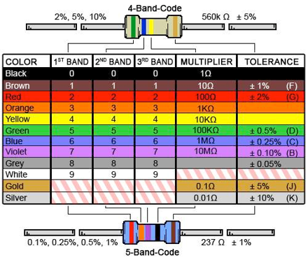
Figure 6.1.2. Resistor color code. https://en.wikipedia.org
Observation: All resistors produce white (thermal) noise.
6.1.2. Capacitors
Similarly, capacitors come in a wide variety of sizes and tolerances. Polarized capacitors operate best when only positive voltages are applied. Nonpolarized or bipolar capacitors operate for both positive and negative voltages. We select a capacitor based on the following parameters: capacitance value, polarized/nonpolarized, maximum voltage level, tolerance, leakage current (resistance), temperature coefficient, useful frequency response, and temperature range. The maximum voltage rating is important for high voltage circuits, but it is of lesser importance for embedded microcontroller systems. Figure 6.1.3 shows some of the available capacitor types. Table 6.1.2 compares various capacitor types we could use in our circuit. Ceramic capacitors are labelled with three digits xyz; the capacitance is xy*10z pF. For example, 473 means 47*103 pF = 47 nF. We will use capacitors for two purposes in our microcontroller-based embedded systems: power line filters (Section 6.2) and analog circuit filters (Section 6.5).
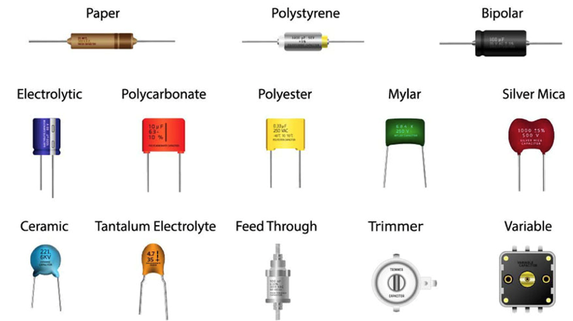
Figure 6.1.3. Capacitor types https://www.ourpcb.com/bypass-capacitor.html.
|
Type |
Range |
Tolerance |
Temp coef |
Applications |
|
C0G/NP0 Ceramic |
0.1pF to 0.47µF |
±1% |
Excellent |
Analog signal processing |
|
X7R/Y5V Ceramic |
10 pF to 47µF |
-20 to +80% |
Good |
Decoupling |
|
Polypropylene |
100pF to 10µF |
Excellent |
Good |
Analog signal processing |
|
Tantalum |
0.1µF to 220µF |
±10% |
Poor |
Bulk decoupling |
|
Electrolytic |
0.47µF to 0.01F |
±20% |
Ghastly |
Bulk decoupling |
Table 6.1.2. General specification of various types of capacitor components (Analog Engineer's Pocket Reference, Art Kay and Tim Green editors, Texas Instruments, 2014).
: A ceramic capacitor is marked 105. What value is it?
DC power line filters: A voltage supply typically includes ripple, which is added noise on top of the desired DC voltage level. We will place capacitors on the DC power lines to filter the supply voltage. There are two physical locations to place the supply filters. The first location is at the entry point of the supply voltage onto the circuit board. There are two approaches to this board-level filter. If the supply noise is mostly voltage ripple, then two capacitors in parallel can be used. The large amplitude polarized capacitor (e.g., 1 to 47 µF electrolytic or tantalum) will remove low frequency large amplitude voltage noise, and the nonpolarized capacitor (e.g., 0.01 to 0.47 µF ceramic) will remove high frequency voltage noise. Two different types of capacitors are used because they are effective (i.e., behave like a capacitor) at different frequencies.
The ∏ filter (CLC) is very effective in removing current spike noise. The CLC parameters depend on the amplitude of the current ripple. The inductor in Figure 6.1.4 can be a ferrite bead. At DC the bead is essentially a short current. The ferrite bead increases both its real and reactive impedance at high frequencies. The bead should be selected to have large impedance at the digital clock frequency. The Panasonic EXC-ELDR25C has a DC resistance of 0.08 Ω, can conduct 7A DC, but has an 80-Ω impedance at 24 MHz. The inductance prevents noise ripples at the frequency of the bus clock from affecting analog circuits also powered with the same +3.3V supply.
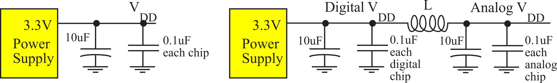
Figure 6.1.4. DC supply filters.
: Why do we use two capacitors (10uF and 0.1uF) on the DC supply filter?
: When does an inductor behave like an open circuit, and when does it behave like a short circuit?
The second location for power-line filters is at the supply pins of each chip. It will be important to place these capacitors as close to the pin as physically possible as illustrated in Figure 6.1.5. A nonpolarized capacitor (e.g., 0.01 to 0.1 µF ceramic) will smooth the supply voltage as seen by the chip. Placing the capacitor close to the chip prevents current surges from one chip from affecting the voltage supply of another.
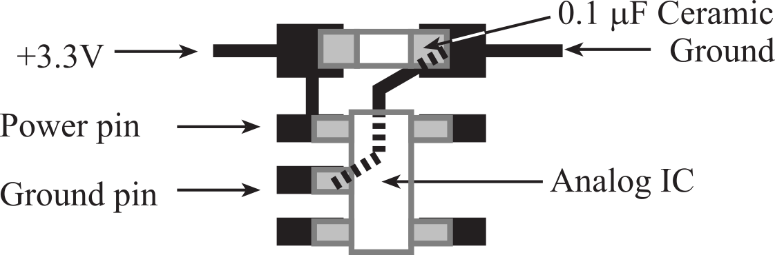
Figure 6.1.5. PCB layout positioning the bypass capacitor close to the chip.
Analog Filters: We will also use capacitors in
designing linear analog circuits. Examples include the low pass filter, the
high pass filter, the derivative circuit, and the integrator circuit. For these
applications we will select a nonpolarized capacitor even if the signal
amplitude is always positive. In addition, we usually want a low-tolerance, low-leakage
capacitor to improve the accuracy of the linear analog circuit.
Ceramic capacitors are a low-cost medium-quality choice for analog circuit
design. They come in many types, see Table 6.1.3 and Figure 6.1.6. K is defined as
C = K e0A/d
where e0 is 8.85 x 10⁻¹² F/m, A is area (m2), and d is distance (m).
The best ceramic is C0G, which has a 1 to 10% tolerance and a temperature
coefficient of 30ppm/oC or ±0.3% over -55 to 125oC. The
middle grade is X7R ceramic, which has a 5 to 20% tolerance and a temperature
coefficient of ±15% over -55 to 125oC. The lowest cost ceramic is Z5U,
which has a 20% tolerance and a temperature
coefficient of 22 to -56% over 10 to 86oC. We can use Z5U for bypass
capacitors on power lines, but we should use either C0G or X7R
for analog filters. For more information on analog filters see Section 6.5.
|
Part number |
Type |
Tolerance |
Cost |
|
06035A102FAT2A |
C0G |
±1% |
$0.118 |
|
06035C102JAT2A |
X7R |
±5% |
$0.052 |
|
06035C102KAT2A |
X7R |
±10% |
$0.023 |
Table 6.1.3. Cost of AVX ceramic capacitors: 1000 pF, 50 V, surface mount 0603 package (2025 prices on www.mouser.com for quantity 10).
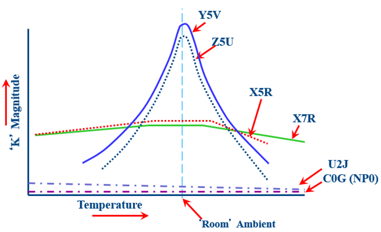
Figure 6.1.6. Temperature dependence for capacitor types.
Capacitor Model: We can model a capacitor as a series combination of capacitance, resistance, and inductance, see Figure 6.1.7.
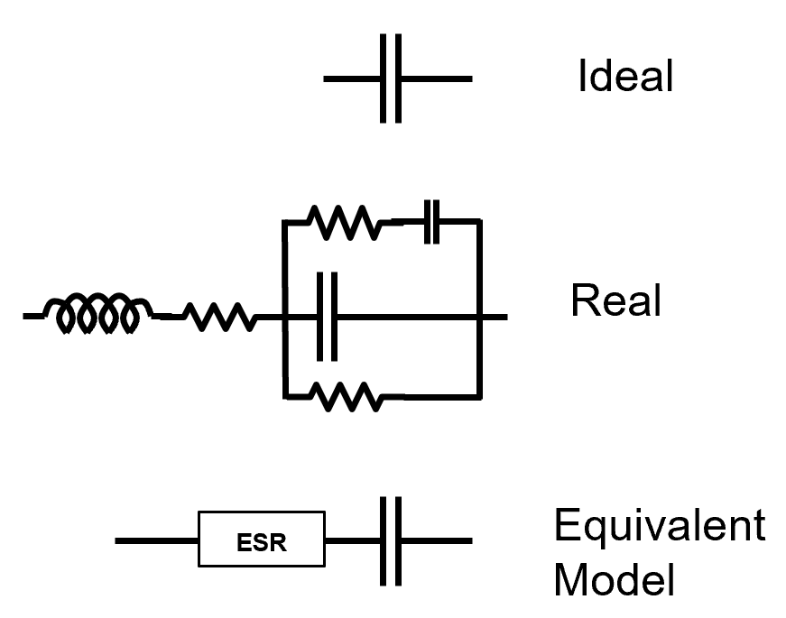
Figure 6.1.7. Capacitor models.
A 10-µF ceramic capacitor has an equivalent series resistance (ESR) of 4 mΩ. The tantalum capacitor has an ESR of 0.1Ω and the electrolytic cap has an ESR if 1Ω. In this analysis all three have an equivalent series inductance (ESL) of 200pH. Figure 6.1.8 shows the effect of ESL and ESR on capacitor frequency response. The solid line is an ideal capacitance with impedance of 1/(2π*f*C). Above 5 MHz the inductance is seen in the ceramic capacitor.
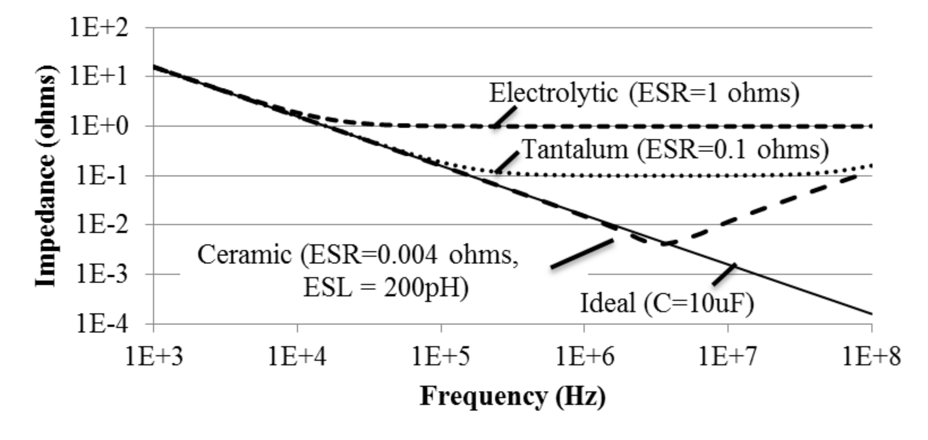
Figure 6.1.8. Impedance of a 10 uF capacitor as a function of frequency (R+1/(2πfCj)+ 2πf Lj).
6.1.3. Tolerance
The first step in effective communication is establishing a clear agreement on the definition of terms. Broadly put, tolerance means putting up with error. However, the dictionary definitions of tolerance and error are not adequate for engineering design as listed in Table 6.1.4. From an engineering perspective, tolerance is the quantitative difference between the desired parameter and the actual value. For example, a ±1% 1000Ω resistor may have an actual value from 990Ω to 1010Ω. Sometimes a parameter is listed as the minimum and maximum values. For example, the offset voltage of an OPA2350 op amp will be between -500 and +500 µV. Specifying tolerance will have a profound impact on both price and performance. If we over-specify (use 1% resistors when 5% would have been OK), then the system costs increase. However, if we under-specify (use 5% resistors for a system needing 1%), then some of the devices we manufacture will not operate properly.
|
Tolerance 1) a fair, objective, and permissive attitude toward those whose opinions, practices, race, religion, nationality, etc., differ from one's own; freedom from bigotry.
2) a fair, objective, and permissive attitude toward opinions and practices that differ from one's own.
3) interest in and concern for ideas, opinions, practices, etc., foreign to one's own; a liberal, undogmatic viewpoint.
4) the act or capacity of enduring; endurance: My tolerance of noise is limited.
5) Medicine/Medical, Immunology. a) the power of enduring or resisting the action of a drug, poison, etc.: a tolerance to antibiotics. b) the lack of or low levels of immune response to transplanted tissue or other foreign substance that is normally immunogenic. |
Error 1) a deviation from accuracy or correctness; a mistake, as in action or speech: His speech contained several factual errors.
2) belief in something untrue; the holding of mistaken opinions.
3) the condition of believing what is not true: in error about the date.
4) a moral offense; wrongdoing; sin.
5) Baseball. a misplay that enables a base runner to reach base safely or advance a base, or a batter to have a turn at bat prolonged, as the dropping of a ball batted in the air, the fumbling of a batted or thrown ball, or the throwing of a wild ball, but not including a passed ball or wild pitch.
|
Table 6.1.4. Dictionary definitions of tolerance and error http://dictionary.reference.com
Another factor related to tolerance is temperature coefficient. The properties of most devices will change with temperature. For example, the Temperature Coefficient of Resistance (TCR) is defined as
TCR (ppm/°C) = 106*(R - R25)/(R25*(T - 25°C))
where R25 is the temperature at 25°C, and R is the resistance at temperature T, as T varies from ‑55°C to +125°C.
We will do a simple example illustrating the effect of tolerance on performance. We will consider the LED interface shown in Figure 6.1.9. We assume the VCE of the PN2222 was 0.3V, the desired LED operating point was 1.9V 10mA, and we calculated the resistor value to be (3.3-1.9-0.3V)/10mA = 110Ω.

Figure 6.1.9. An LED I-V curve and an LED interface circuit.
In the operating range of 10mA, the voltage is approximately constant. Thus, the light intensity of the LED is approximately linear with current. So, we will determine the effect of resistor tolerance on LED current. We will investigate an E24 5%-resistor with nominal value of 110 Ω. This resistor can vary from 104.5 to 115.5 Ω, causing the LED current to vary from 9.5 to 10.5 mA. In this case, the ±5% resistance tolerance converted simply to a ±5% variability in light intensity. To consider the effect of tolerance in the PN2222 transistor, we need to know the possible range for VCE. At saturation, the VCE has a maximum of 0.3 V. Assuming the worst case of VCE equal to 0.1 V, the LED current could increase to 11.8 mA. Putting these two effects together is presented in Table 6.1.5. Realistically, the VCE probably varies only from 0.2 to 0.3 V, so the LED current could vary from 9.5 to 11.5 mA, or -5% to +15% from desired.
|
|
VCE = 0.1 |
VCE = 0.2 |
VCE = 0.3 |
|
R=104.5 |
12.4 |
11.5 |
10.5 |
|
R=110 |
11.8 |
10.9 |
10.0 |
|
R=115.5 |
11.3 |
10.4 |
9.5 |
Table 6.1.5. LED current varies with R and VCE.
Table 6.1.5 is a simple two-dimensional analysis. If we added the effect of temperature, then the problem becomes three dimensional. As the number of parameters increases, so does the complexity of the problem. It is important to determine which parameters have the largest effect on output. These parameters will then require lower tolerance. For example, assume the circuit has three resistors (R1, R2, and R3) and the output is the voltage V. Each resistor has an error due to tolerance and/or temperature drift (±δ1, ±δ2, and ±δ3). We could use differential calculus to determine the relative sensitivity to each parameter (S1, S2, and S3). We should focus our money and attention on the parameters having the largest effect on performance. We can calculate the error in V (δV) due to errors in R. Let x be the measurand and let Δx be the desired resolution. Using the sensitivity of V to x (∂V/∂x), we can determine a design metric.
S1 = ∂V/∂R1
S2 = ∂V/∂R2
S3 = ∂V/∂R3
δV = ±(∂V/∂R1)*δ1 ± (∂V/∂R2)*δ2 ± (∂V/∂R3)*δ3
δx = (±(∂V/∂R1)*δ1 ± (∂V/∂R2)*d2 ± (∂V/∂R3)*δ3)/(∂V/∂x) ≤ Δx
: Assume the measurand, x, is distance in cm. Do a dimensional analysis of the above equations. What are the dimensions of S, δV, and δx?
6.2. Power
6.2.1. Regulators
Every embedded system needs power to operate. The source of power could be
120 VAC 60 Hz
DC power, like +5V on USB or +12V in an automobile
Battery
Energy harvesting like solar or EM field pickup
Many embedded systems are powered with an AC adapter. Other names for this adapter that takes 120 VAC in and outputs an unregulated DC voltage include power adapter, power block, wall wart, wall cube, and power brick. A 9-V, 500-mA unregulated AC adapter means the voltage is above 9 V for all currents less than 500 mA. However, the actual voltage can vary considerably. For example, the voltage might range from 13 V at no current down to 9.5V at 500 mA. Similarly, battery voltage is not constant, decreasing with age and use. Therefore, a regulator will be used to provide a constant voltage to power the system. In this section, we will introduce two types of regulators: linear and switching. There are many considerations when choosing a regulator, and we will discuss some of these considerations.
Linear regulators take an input voltage, Vin, and create a constant output voltage, Vout. Capacitors on both the input and output are needed to stabilize the linear regulator (Figure 6.2.1). The band gap reference includes a diode to create a constant reference voltage, Vref, in a similar way as the LM4041. The two resistors will sense the output voltage. The sensed output voltage is compared to Vref. The output of the error amp will control the pass element, which is a transistor device whose resistance can be adjusted. It is classified as a linear regulator because the pass element operates in its linear region. The regulator uses feedback to maintain a constant Vout regardless of load current, Iout and input voltage Vin. Some regulators, like the 78x05 series, use a bipolar transistor for the pass element. While other regulators, like LP2981, use a MOSFET for the pass element. In either case, current can only flow from input to output across the pass element, meaning Vin must be greater than Vout. Furthermore, because the pass element is resistive, power will be lost as voltage drops across the regulator. The quiescent current of a regulator, Iq, is the current needed to operate internal functions of the regulator, like the band gap reference.
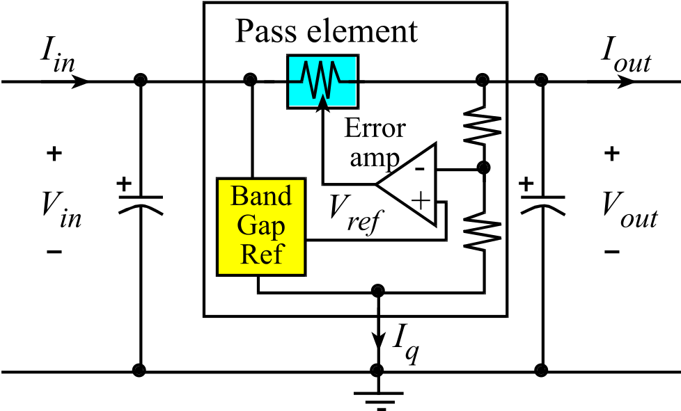
Figure 6.2.1. Architecture of a linear regulator.
Linear regulators need an input voltage, Vin, larger than the output voltage, Vout. If the current is Iout, then power is lost in the regulator and dissipated as heat in the amount of Pd = (Vin‑Vout)*Iout. Linear regulators have a voltage dropout, Vdo, which specifies how much higher Vin needs to be above Vout for it to work. The dropout voltage for the 5-V 78L05 regulator is 2 V, meaning Vin must be larger than +7 V for the output to be +5V. Conversely, the dropout voltage for the LP2981 is only 0.2 V. For example, a 3.7-V Li‑ion battery with a LP2981-3.3 regulator could be used to power a 3.3 V system. Regulators with a low dropout voltage are classified as LDO regulators. Figure 6.2.2 shows some circuits based on linear regulators. Because of the resistive nature of the pass element, linear regulators are not very efficient. The efficiency is defined as the output power divided by the input power:
η = (Vout * Iout)/(Vin * Iin) = (Pout)/(Pout + Pd)
|
Regulator |
Iout |
Vdo |
Iq |
|
500 mA |
1.45 V |
10 mA |
|
|
800 mA |
1.2 V |
5 mA |
|
|
100 mA |
0.38 V |
75 µA |
|
|
100 mA |
0.2 V |
0.6 mA |
|
|
150 mA |
0.13 V |
500 nA |
Table 6.2.1. Typical parameters for some 3.3-V linear regulators.
: What is the difference between input and output current for LP2950-3.3?
: Which regulators in Table 6.2.1 can we use to create 3.3V supply from a 3.7V battery?
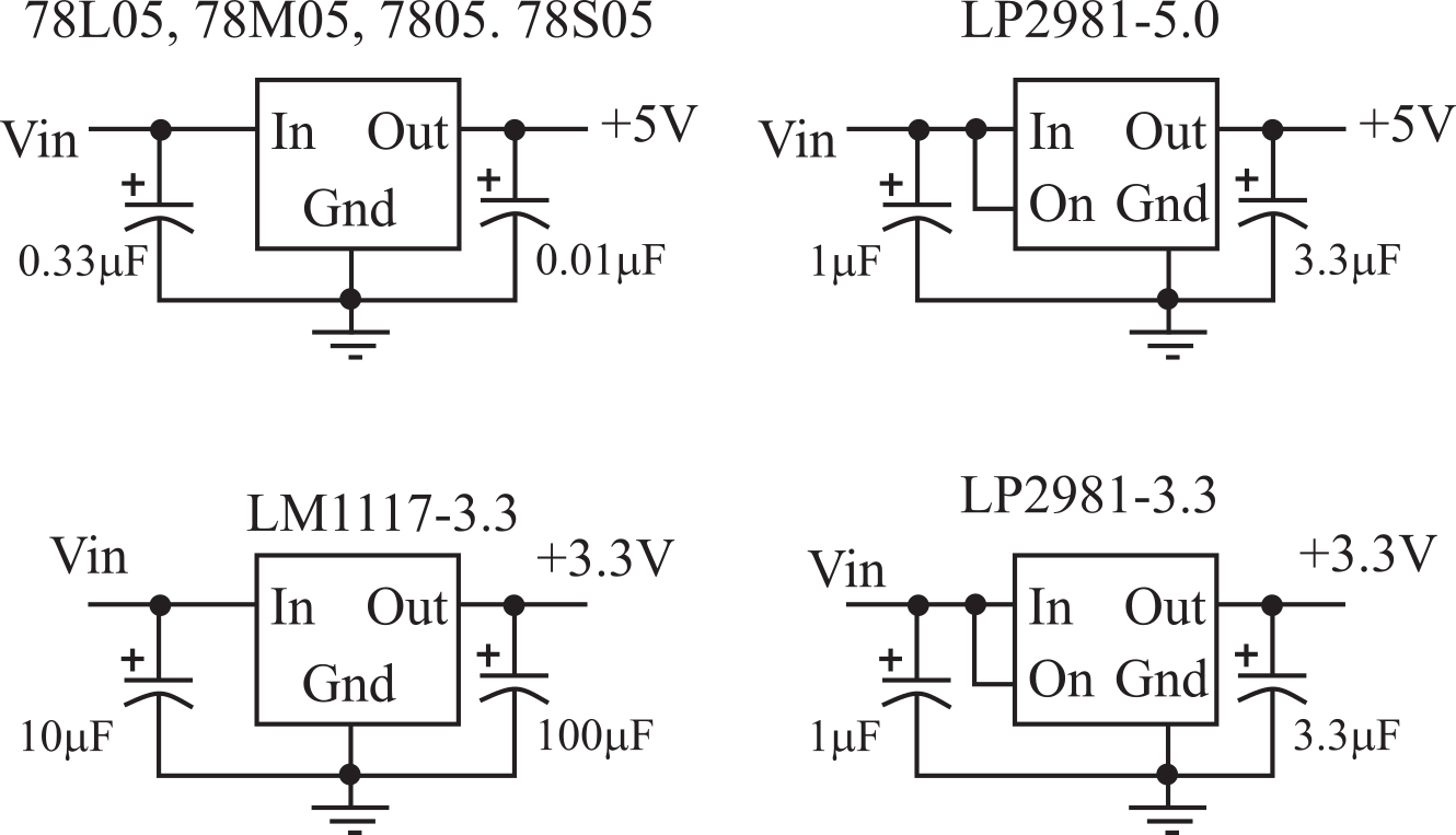
Figure 6.2.2. Linear regulator circuits.
Observation: With linear regulators, the input and output currents are approximately equal.
To improve efficiency and provide flexible input voltage, there is a class of regulators that use an inductor and a switching circuit to create a constant output voltage. Three types of switching regulators are shown in Figure 6.2.3. A buck regulator uses a switch at the input to dump power into an LC circuit. Like the linear regulator, a buck regulator requires the input voltage to be larger than the output voltage. A boost regulator rearranges the switch and inductor, but it also uses the switch to dump power into an LC circuit. When the switch is open power flows into the capacitor; when the switch is closed power is stored on the inductor. A boost regulator can only be used in situations where the input voltage is less than the output voltage. A buck-boost regulator uses a method called flyback so the output voltage can be regulated regardless of whether the input voltage is larger or smaller than the desired output. In each case, the duty cycle of the switch is controlled so that the output voltage remains constant. Assuming ideal components these switching regulators will be 100% efficient.
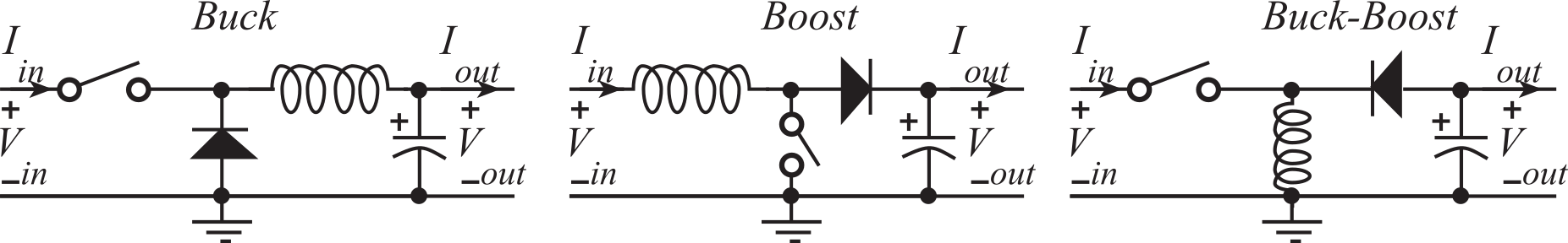
Figure 6.2.3. Architecture of a switching regulator.
The TPS63001 and TPS63002 buck-boost regulators operate with inputs from 1.8 and 5.5 V. The LM2596S-5.0 buck regulator will create a +5-V output if the input is between 7 and 40 V.
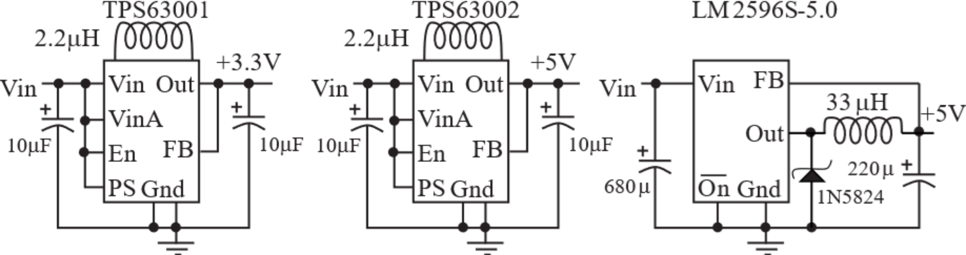
Figure 6.2.4. Switching regulator circuits. The LM2596S-5.0 comes in a form easy to solder.
: Portable cellphone charges have a 3.7V Li-ion battery and output 5V. Which regulator(s) in Figures 6.2.2 and 6.2.4 could it use?
Buck-boost regulators are rated for their efficiency and have a sizeable high frequency switching noise in the power line. The frequency of the noise depends on how the buck-boost regulator is built. Since linear regulators have lower noise, they are more suitable for precision analog electronics. Noise on Vout can come from the input, like the 60 Hz ripple from a 120 VAC transformer, or noise can come from within the regulator, like the switching regulator. Let Vinrms be the rms AC amplitude on the input, and Voutrms be the rms AC amplitude at the output. Power supply rejection ratio (PSRR) is the amount of ripple on the input that is transferred to the output.
PSRR = 20 * log10(Vinrms/Voutrms)
Regulators can be fixed output (e.g., 3.3 or 5 V) or adjustable. Adjustable regulators use two resistors to set the output voltage level. Many regulator families have both fixed output and adjustable versions such as LM1086, LM1117, LT1761, TPS63000, and TPS63060. Adjustable regulators are convenient if the system needs to have a user-controlled switch to decide whether the system is powered at 3.3 or 5 V. We choose a regulator that has a maximum current larger than the current requirements of the system. For example, the maximum currents for the 78L05, 78M05, 7805, and 78S05 are 100 mA, 500 mA, 1 A, and 2 A, respectively. The line regulation parameter specifies how the output voltage will vary as a function of input voltage. The load regulation parameter specifies how the output voltage will vary as a function of the current to the system. Table 6.2.2 characterizes the strengths of a linear versus switching regulator.
Observation: Regulators are very different from each other, so it is essential to read the data sheet and follow all the design recommendations concerning external components, heat sinks, and layout.
|
Linear Regulator |
Switching Regulator |
|
Small size |
High efficiency |
|
Low noise, low output ripple |
Wide range of input voltage |
|
Simple design |
Vout less than or greater than Vin |
|
Fast transient response |
Low power dissipation (small heat sink) |
|
Low quiescent current Low cost Good PSRR No EMI emissions |
Can have multiple output voltages With a transformer, could be isolated Best for large currents |
Table 6.2.2. Advantages of regulator types.
The TM4C microcontrollers need a regulated 3.3-V supply voltage. However, many microcontrollers will operate on a wide range of supply voltages
MSP430L092 will run on supply voltage from 0.9 to 1.65V
MSP430F20x2 will run on supply voltage from 1.8 to 3.6V
MSPM0G3507 will run on supply voltage
from 1.62 to 3.6V
For some applications it may be possible to run the system directly off a battery without a regulator. Without regulated power, these systems will have more variability in bus clock frequency and analog voltage. However, without a regulator the system can be smaller, lower cost, and by design it will be 100% battery efficient.
Observation: Iq is important when putting a microcontroller into deep sleep for a long time.
Many analog IC manufacturers provide design tools. WebBench is a free design tool from Texas Instruments you can use to design power supply circuits (https://www.ti.com/tool/WEBENCH-CIRCUIT-DESIGNER). Using these design tools you will be able to create supply circuits much better than the ones presented in this book.
6.2.2. Battery Power
A battery is a source of energy that can be used in an embedded system to make the system portable. Another application of batteries is to supply power to a mission-critical system when the regular AC power is lost temporarily. Typically, a battery has three parts. The anode is the negative terminal of the battery, the cathode is the positive terminal, and the electrolyte is a liquid solution that accepts stores and releases energy. These three components can be constructed from many different materials and configured in an almost endless array of sizes and shapes. The type, size, and shape of the materials play a major role in determining the battery performance. A primary battery is used once and discarded, and a secondary battery can be recharged and reused.
There are many parameters to consider when selecting a battery. Nominal voltage is the typical voltage of the battery when fully charged. Some batteries maintain a constant voltage output while energy is being discharged. However, other batteries will drop the voltage steadily during usage. Physical parameters of the battery (such as volume, weight, and shape) often play a significant role in the overall appeal of an embedded system. Peak current is the maximum current the battery can deliver. Shelf-life, operating temperature, and storage temperature are other parameters to consider when choosing a battery. Memory effect is an observable condition in some rechargeable batteries that causes them to hold less charge over time. The energy storage of a battery is typically defined in amp-hours, because the voltage is assumed to be constant. The standard units of energy are watt-hours (1 W-hr is 3600 J). One can estimate the operation time of a battery-powered embedded system by dividing the energy storage by the average current required to run the system. The power budget embodies this concept. Let E be the battery specification in amp-hours and tlife be the desired lifetime of the product; then we can estimate the average current our system is allowed to draw:
Average Current ≤ E/tlife
: A medical device implanted inside the body has a 500 mA-hour battery that must last 5 years. What is your power budget?
Heavy-duty batteries, were first made with zinc-carbon in the mid-1800s, but now are made with zinc chloride. They are a low-cost, low-performance battery but are not appropriate for most embedded applications. An alkaline battery is made with alkaline manganese. Alkaline batteries are appropriate for situations that require long shelf life, but size and weight are not important. There are two kinds of lead acid batteries. Flooded lead-acid vent inflammable gasses and require additional water to maintain the proper specific gravity of the acid. Valve-regulated lead-acid (VRLA also called sealed lead battery) have about a two-to-one advantage over the flooded type battery in specific energy and energy density. In the VRLA cell, the vent for the gas space incorporates a pressure relief valve to minimize the gas loss and to prevent direct contact between the headspace and outside air. Lead acid batteries can be used for backing up power on systems that require large currents. Lead acid batteries have a maximum storage time of six months at temperatures between 20 and 30°C, after which they require a freshening charge. Zinc chloride, alkaline, and lead-acid batteries all have voltages that drop as energy is drained from them. In these systems, the voltage can be monitored as a measure of the energy left in the battery. However, embedded systems that use these types of battery will require a voltage regulator to maintain a constant voltage for the electronics. For example, the MSP430 microcontroller will operate with a power supply voltage anywhere from 1.8 to 3.6 V. The TM4C microcontrollers will run with a supply voltage from 3.0 to 3.6 V.
Nickel-cadmium (NiCad) and nickel-metal hydride (NiMH) are low-cost rechargeable batteries that used to be popular for embedded systems. NiMH batteries have about twice the storage capacity as NiCad. Certain NiCad batteries gradually lose their maximum energy capacity if they are repeatedly recharged after being only partially discharged. Most NiMH batteries do not suffer from a memory-effect. The NiMH batteries operate between 10 to 55°C, and have a projected life of seven and a half years at 30 °C. You should cycle new NiMH batteries three to five times to achieve peak performance. Cycling or conditioning a NiMH battery is performed by completely discharging it then completely recharging it. At room temperature, NiMH batteries will self-discharge in 30 to 60 days without usage, depending on environmental conditions. In general, you can expect NiMH batteries to last up to 500 recharges.
The search for a lighter battery that uses metallic lithium as its anode was driven by the fact that lithium is the lightest and the most electropositive of metals. The specific energy of lithium metal (1727Ah/lb) is greater than lead (118Ah/lb) and cadmium (218Ah/lb). There are a whole range of batteries based on Lithium, both single use (used in cameras) and rechargeable. The most common rechargeable type is called Lithium-ion (Li-ion). When energy is being discharged, the lithium ion moves from the anode to the cathode. During charging, the lithium ion moves from the cathode to the anode. Because of their excellent energy-to-weight and energy-to-size ratios, Lithium-ion rechargeable batteries are commonly employed in portable embedded systems. Table 6.2.3 shows energy storage for typical AA-sized batteries (50 mm tall by 14 mm diameter). Table 6.2.4 lists some Li-ion rechargeable batteries.
|
Battery |
Voltage (V) |
Energy (mAh) |
Type |
|
Alkaline |
1.5 |
2000 |
Primary |
|
Lithium |
1.5 |
3000 |
Primary |
|
NiCad |
1.2 |
1200 |
Secondary |
|
NiMH |
1.2 |
1800 |
Secondary |
|
Li-ion |
3.6 |
1900 |
Secondary |
Table 6.2.3. Energy storage for different AA-sized battery types.
|
Battery |
Shape |
Energy (mAh) |
Size (mm) |
Weight (g) |
|
GMB power GM041124 |
Thin Pack |
60 |
4.0 × 11 × 24 |
1.2 |
|
GMB power GM041429 |
Thin Pack |
120 |
4.0 × 14 × 29 |
2.8 |
|
GMB power GM041842 |
Thin Pack |
250 |
4.0 × 18 × 42 |
5.5 |
|
TrustFire 10440 |
AAA |
600 |
10.25 × 46.25 |
9.5 |
|
UltraFire 14500 |
AA |
900 |
14 × 50 |
31 |
|
Tenergy 30027 |
Cylinder |
2200 |
69 × 19 |
54 |
|
Tenergy 31000 |
Pack |
4400 |
65 × 37 × 18 |
170 |
|
Tenergy 31002 |
Pack |
6600 |
69 × 54 × 18 |
255 |
Table 6.2.4. Example 3.7 V Li-ion batteries ( http://www.powerstream.com/ http://www.gmbattery.com/ http://www.batteryjunction.com/).
: A medical device implanted inside the body has an average current 20 µA and must last for 1 year. Which battery in Table 6.2.4 would you choose?
To make the system more convenient, battery-powered embedded systems could include a built-in recharger. The system can run and charge while plugged in. However, it will also run off the battery when AC power is not available. There are many battery charging circuits available. Figure 6.2.5 shows a charging circuit a NiMH battery. R1 is depends on the smallest Vin from the wall cube. If Vin is larger than 10 V, the set R1 = (10-5V)/5mA = 1 kΩ. R3 and R4 are part of a thermal shut-down safety circuit, which is not implemented in this simple version. The Rsense resistor sets the fast programming current: Ifast = 2.5V/Rsense, which is 1 A for this circuit. The PGM0, PGM1, PGM2, and PGM3 pins specify the charging protocol and the number of NiMH cells, which is 7 cells or 8.4 V for this circuit.
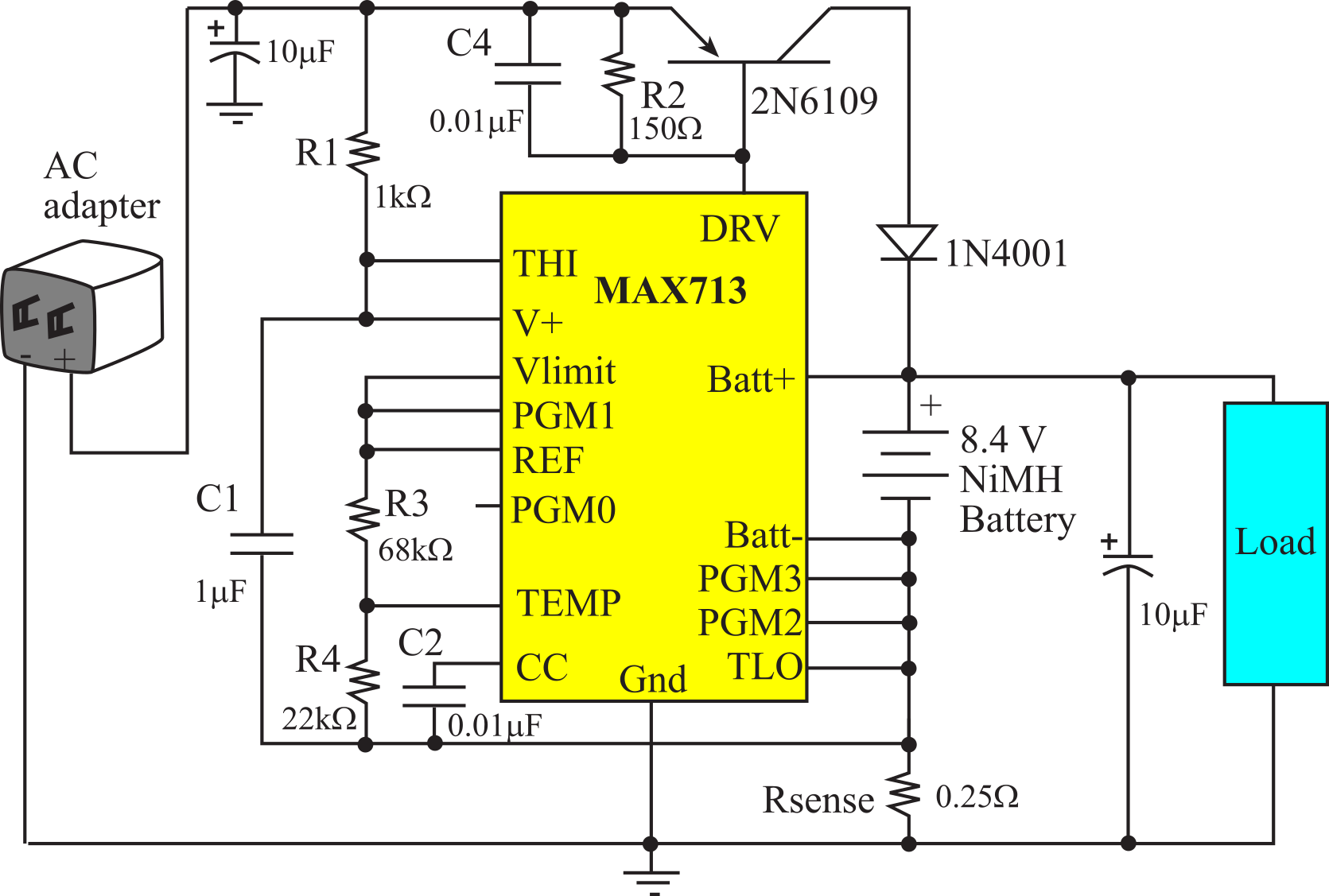
Figure 6.2.5. Charging circuit for an 8.4-V NiMH battery with a 1-A charging current using a MAX713.
Figure 6.2.6 shows a charging circuit for a Li-ion battery. You should refer to the specific datasheets to work through the resistor and capacitor values depending on the voltage and current of the battery.
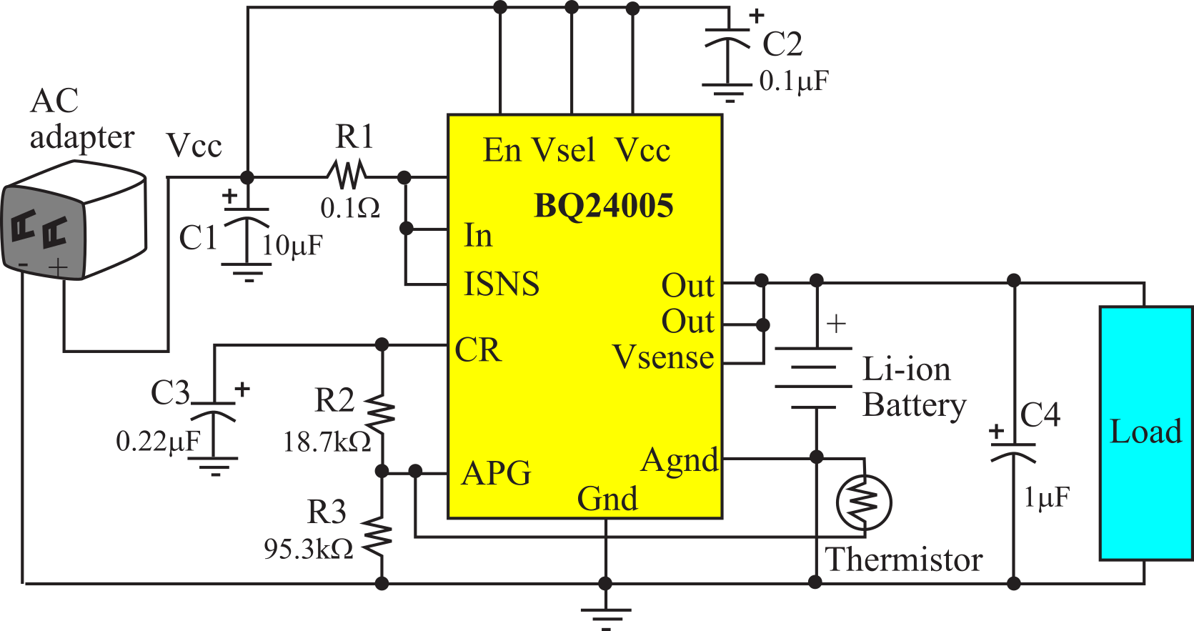
Figure 6.2.6. Charging circuit for a 7.2-V Li-ion with a 1.2-A charging current using a BQ24005.
6.2.3. Current Measurement
To evaluate the performance of a low power system we need a method to measure supply current on the actual system. A simple method would be to charge up a battery with known energy storage and measure how long the battery runs the system.
There are a couple of circuits that could be used to measure current, allowing us to visualize supply current versus time. If a +5V supply is available, we could use an instrumentation amplifier as shown in Figure 6.2.7. In this example, we expect the current to be less than 30 mA, so a shunt resistance of 2Ω is selected, because the 3.3V supply will only drop to 3.24V and not affect system operation. Since the instrumentation amp is powered with 5V and ground, the voltages at the two inputs (pins 2 and 3) will be around 3.3V operating the amp in its linear region. If the supply current is 30 mA, the output voltage will be 2.68V. When using this circuit, we need to calibrate the measurement by using three or four precision resistors in place of the system.
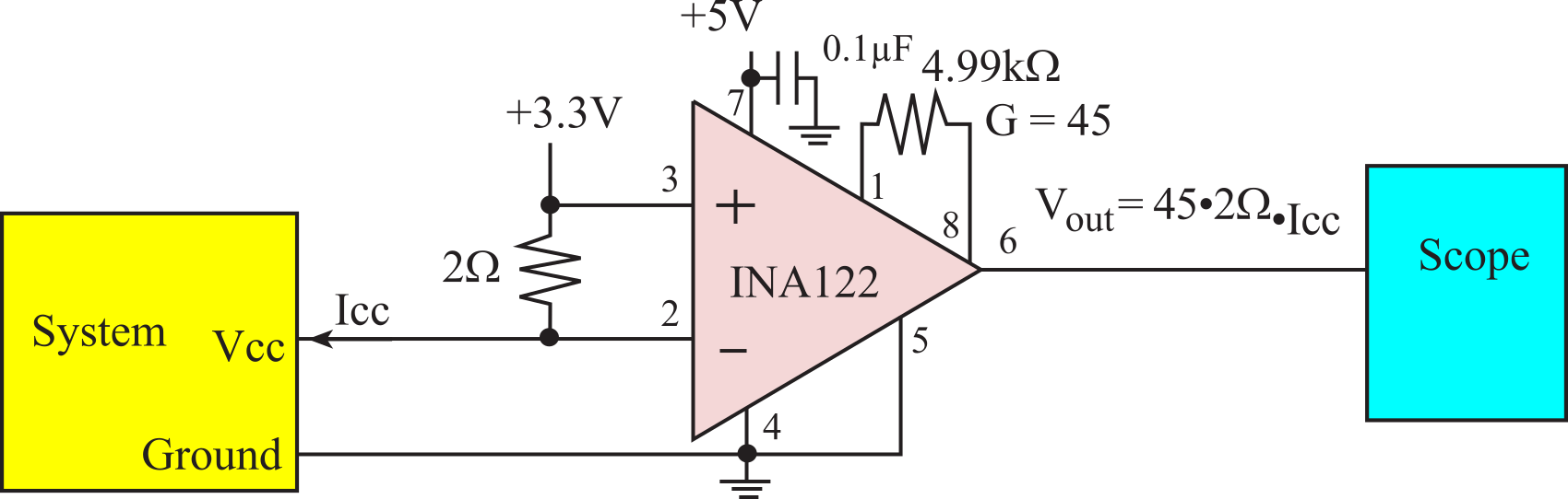
Figure 6.2.7. Circuit used to measure supply current, Icc using an INA122.
To illustrate the use of Figure 6.2.7, two TM4C123 systems were designed. Both systems toggled an output pin every 5 seconds. Both systems ran on the internal oscillator at 16 MHz. The first system used SysTick and the second one used hibernation to enter deep sleep while waiting the 5 seconds. Program 6.2.1 shows the low-level software to hibernate. The real time clock (RTC) is programmed to wake up the processor in a specified number of seconds. Since the hibernation module runs on the 32768Hz external crystal, the software must wait for the WRC bit in the CTL register after every access. Initialization turns on the hibernation module and connects to the 32768Hz clock. The VDD3ON bit is set so the digital outputs remain powered while sleeping. To start hibernation we set the match time in RTCM0, clear the RTC counter, and issue a hibernation request. It takes some time to activate, so the dummy for-loop is added to the execution never returns from hibernation.
void static HIBready(void){
while((HIB_CTL_R&0x80000000)==0){}; // wait for WRC, Write Complete
}
void HIB_Init(void){
SYSCTL_RCGCHIB_R |= 0x01;
while((SYSCTL_PRHIB_R&0x01)==0){}; // wait for clock
HIBready(); HIB_CTL_R = 0x40; // CLK32EN Hibernation module clock
HIBready(); HIB_CTL_R = 0x140; // VDD3ON internal switches
}
void HIB_Hiberate(uint32_t seconds){ int i;
HIBready(); HIB_RTCM0_R = seconds; // time to sleep
HIBready(); HIB_RTCSS_R = 0; // no subseconds time
HIBready(); HIB_RTCLD_R = 0; // clear RTC counter
HIBready(); HIB_CTL_R = 0x014B; // go to sleep
for(i=1000;i;i--){}; // this should not finish
}
void HIB_SetData(uint32_t data){
HIBready(); HIB_DATA_R = data; // save important information
}
uint32_t HIB_GetData(void){
HIBready();
return HIB_DATA_R; // recover data
}
Program 6.2.1. Software to put the microcontroller into deep sleep (HIB_4C123).
Program 6.2.2 shows two high-level programs that toggle an output pin every 5 seconds. The one on the left uses SysTick and requires a continuous 10.1 mA to operate. The program on the right uses hibernation. When the software wakes up from hibernation, it begins execution at the reset vector. However, there are 16 words (64 bytes) of backup RAM that can be used to remember data after hibernation. The SetData and GetData functions allow the user to save and restore information in the first of these 16 words (HIB_DATA_R). In this example, the number of times the system has been awakened is stored in this backup RAM. If the count is odd the output is set high, and if the count is even the output is cleared low. It takes about 10.4 ms to execute this simple program, during which time the processor used about 5 mA of current. However, in deep sleep for 4.99sec, the system only draws 0.1 mA. Figure 6.2.8 plots the instantaneous current during the wakeup. Notice the current surge occurring during the initial wakeup.
|
int main(void){ |
int main(void){ uint32_t count; |
Program 6.2.2. System that toggles an output every 5 seconds (HIB_4C123).
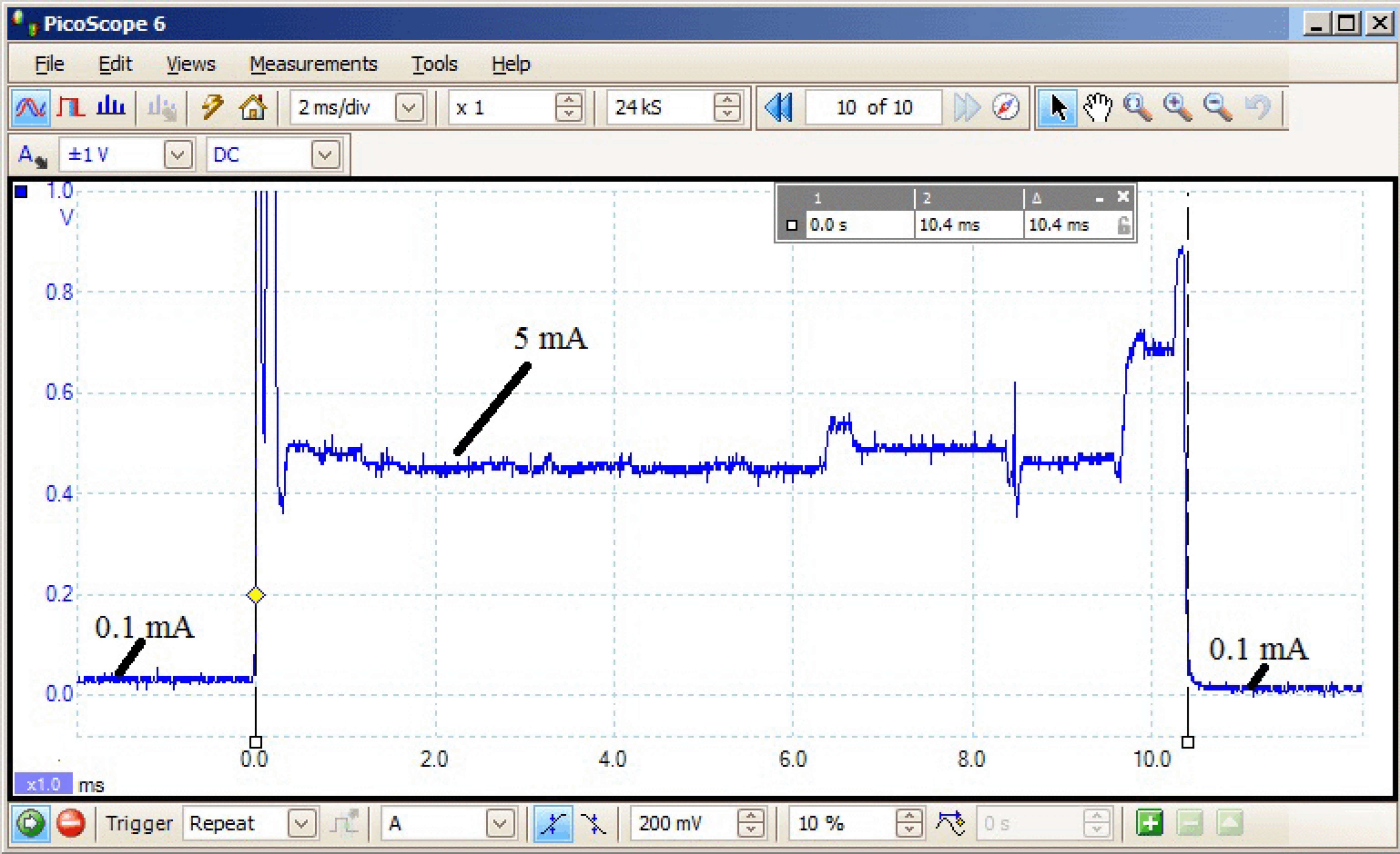
Figure 6.2.8. Instantaneous current measured versus time measured with the circuit in Figure 6.2.7. This measurement was taken on a TM4C123 LaunchPad. Icc = V/90.
Observation: The hibernation system executes about 50 lines of C code each time it runs. The processor is running at 16 MHz. However, because the HIB module runs on the 32kHz clock, these 50 lines require 10.4 ms to execute.
Figure 6.2.7 was also used to study the effect of the PLL on supply current. In each system, the TM4C123 LaunchPad was used to create a periodic interrupt that toggled an output pin. Running the system at 16 MHz with the internal oscillator required an average current of 3.5 mA, while running the system at 16 MHz with the PLL required 8 mA.
Next, the system was run at a range of bus frequencies without WFI. Then the same frequencies were run a second time, but with a WaitForInterrupt (WFI), which powers down some of the processor while waiting for the interrupt. Figure 6.2.9 shows the effect of bus frequency and WFI.
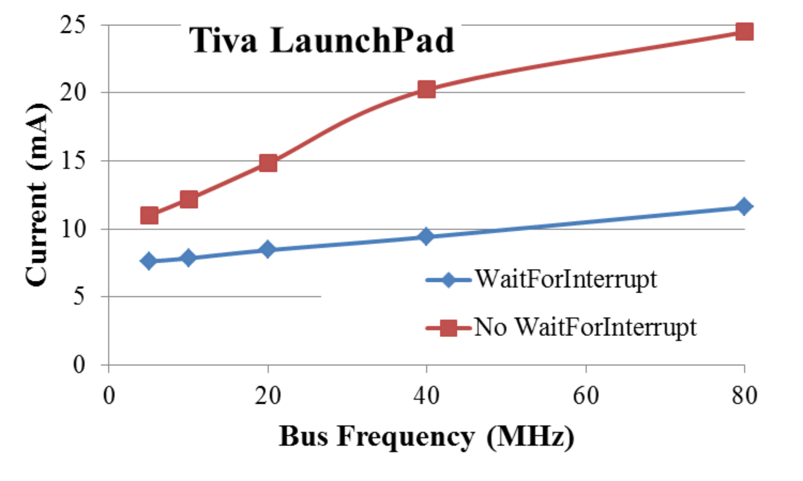
Figure 6.2.9. System current depends on bus frequency and one can save power by executing WFI when waiting for an interrupt. The measurements were performed on a TM4C123 LaunchPad with the PLL active.
: What how much power do you save using hibernation at 32kHz as compared to wait-for-interrupt at 80 MHz?
Sometimes one wishes to measure current but there is no extra supply voltage like the +5V supply used in Figure 6.2.10. For this situation we can use a current sense amplifier that is specifically designed to collect power off the same supply with which we are measuring current. The circuit in Figure 6.13 will measure supply current up to 5V yielding a linear output from 0 to 100 mV. Again, it uses a shunt resistor to create a voltage linear with current. For large currents we should use a Kelvin 4-terminal shunt resistor to improve accuracy. However, this circuit is specially designed to operate linearly enough though the input voltages are right at the rail (near 3.3V). Gain is determined by the resistor ratio, 4999/100 = 50.
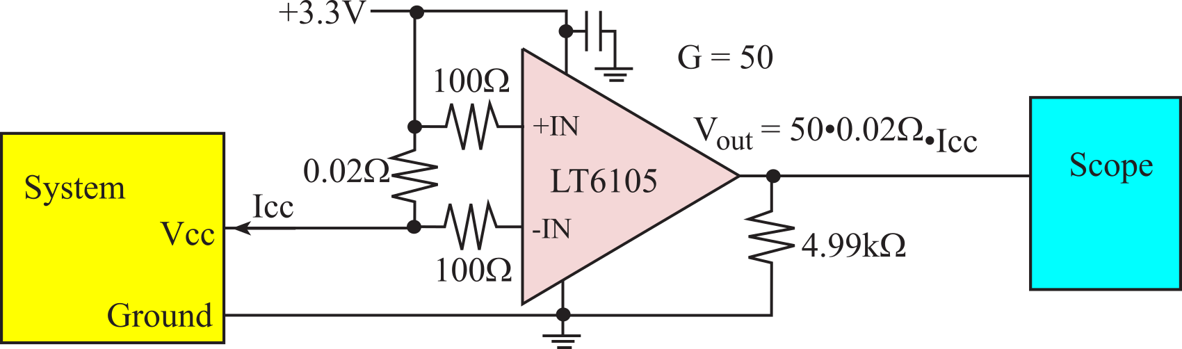
Figure 6.2.10. Current sense amplifier used to measure supply current, Icc using an LT6105.
6.2.4. Grounding
In some medical and industrial applications, we need to design analog instrumentation that is isolated from earth ground. In an industrial setting, isolation is one way to reduce noise pickup from large EM fields produced by heavy machinery. In medical applications we need to protect the patient from potentially dangerous microshocks, Thus, the medical instrument must be isolated. There are three approaches to isolation, as shown in Figure 6.2.11. In the first approach, shown at the top of Figure 6.2.11, an analog isolation barrier is created between the preamp and amp. This was the original approach used in analog instruments before the advent of mixed analog-digital systems. It is expensive, bulky and introduces a very large transfer error. It is not appropriate for embedded applications that use a microcontroller. In the second approach, we use digital isolation. The ADUM2400/2401/2402 air-core transformers are effective low-cost mechanisms to implement digital isolation. This is the most common approach used for new designs when a hard connection between the data acquisition system and building is required. It is fast, small, cheap, and will not cause errors. The third approach runs the entire system with batteries, using a wireless protocol to connect to other electronics. This is a very attractive approach due to the availability of high-quality low-power LED/LCD displays and wireless networks, such as Bluetooth, ZigBee, and 802.11b.
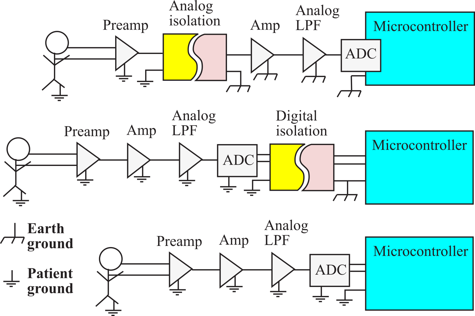
Figure 6.2.11. Analog isolation, digital isolation, and battery-powered all provide protection from microshocks.
6.3. Transistors as Switches
6.3.1. Bipolar Junction Transistors (BJT)
We can use a bipolar junction transistor (BJT) to source or sink current. For most of the circuits in this book the transistors are used in saturated mode. In general, we will use NPN transistors to sink current to ground. We turn on an NPN transistor by applying a positive Vbe. This means when the NPN transistor is on, current flows from the collector to the emitter. When the NPN transistor is off, no current flows from the collector to the emitter. Each transistor has an input and output impedance, hie and hoe respectively. The current gain is hfe or β. The hybrid-pi small signal model for the bipolar NPN transistor is shown in Figure 6.3.1.
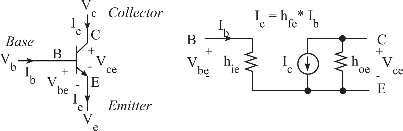
Figure 6.3.1. NPN transistor model.
There are five basic design rules when using individual bipolar NPN transistors in saturated mode:
1) Normally Vc > Ve
2) Current can only flow in the following directions
from base to emitter (input current)
from collector to emitter (output current)
from base to collector (doesn't usually happen, but could if Vb > Vc)
3) Each transistor has maximum values for the following terms that should not be exceeded
Ib Ic Vce and Ic * Vce
4) The transistor acts like a current amplifier
Ic = hfe * Ib
5) The transistor will activate if Vb > Ve + Vbe(SAT)
where Vbe(SAT) is typically above 0.6V
In general, we will use PNP transistors to source current from a positive voltage supply. We turn on a PNP transistor by applying a positive Veb. This means when the PNP transistor is on, current flows from the emitter to the collector. When the PNP transistor is off, no current flows from the emitter to the collector. Each transistor has an input and output impedance, hie and hoe respectively. The current gain is hfe or β. The hybrid-pi small signal model for the bipolar PNP transistor is shown in Figure 6.3.2.
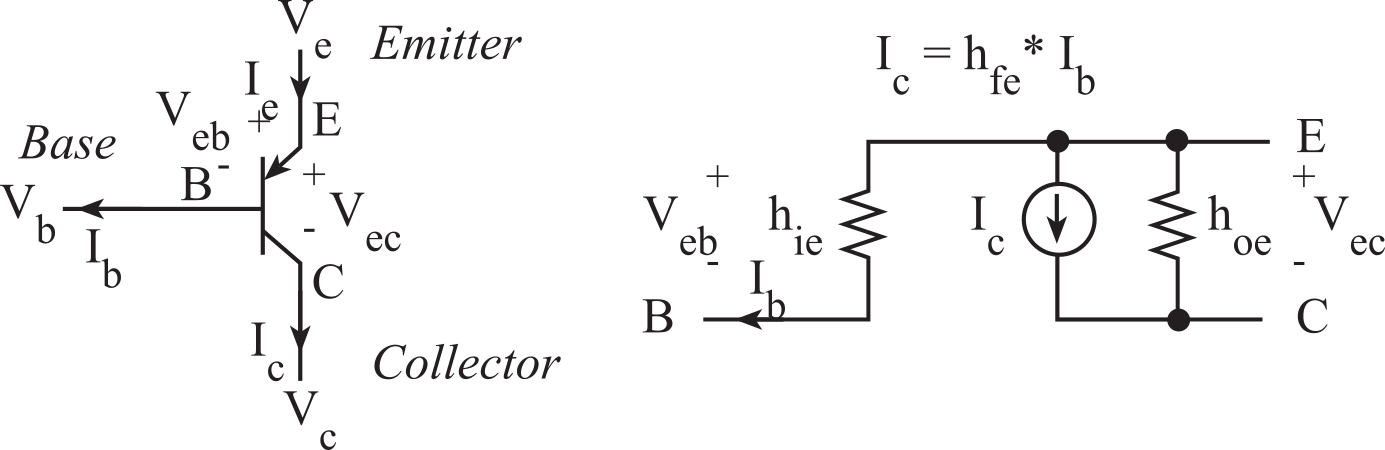
Figure 6.3.2. PNP transistor model.
There are five basic design rules when using individual bipolar PNP transistors in saturated mode:
1) Normally Ve > Vc
2) Current can only flow in the following directions
from emitter to base (input current)
from emitter to collector (output current)
from collector to base (doesn't usually happen, but could if Vc > Vb)
3) Each transistor has maximum values for the following terms that should not be exceeded
Ib Ic Vce and Ic * Vce
4) The transistor acts like a current amplifier
Ic = hfe * Ib
5) The transistor will activate if Vb < Ve - Vbe(SAT)
where Vbe(SAT) is typically above 0.6V
Performance Tip: A good transistor design is one that the input/output response is independent of hfe. We can design a saturated mode circuit so that Ib is 2 to 5 times as large as needed to supply the necessary Ic.
The Table 6.3.1 illustrates the wide range of bipolar transistors that we can use.
|
Type |
NPN |
PNP |
package |
Vbe(SAT) |
Vce(SAT) |
hfe min/max |
Ic |
|
general purpose |
2N3904 |
2N3906 |
TO-92 |
0.85 V |
0.2 V |
100 |
10mA |
|
general purpose |
PN2907 |
TO-92 |
1.2 V |
0.3 V |
100 |
150mA |
|
|
general purpose |
2N2907 |
TO-18 |
1.2 V |
0.3 V |
100/300 |
500mA |
|
|
power transistor |
TIP29A |
TIP30A |
TO-220 |
1.3 V |
0.7 V |
15/75 |
1A |
|
power transistor |
TIP31A |
TIP32A |
TO-220 |
1.8 V |
1.2 V |
25/50 |
3A |
|
power transistor |
TIP41A |
TIP42A |
TO-220 |
2.0 V |
1.5 V |
15/75 |
3A |
|
power darlington |
TIP125 |
TO-220 |
2.5 V |
2.0 V |
1000 min |
3A |
Table 6.3.1. Parameters of typical transistors used to source or sink current.
Under most conditions we place a resistor in series with the base of a BJT when using it as a current switch. The value of this resistor is typically 100Ω to 10kΩ. The purpose of this base resistor is to limit the current into the base. The hie is typically around 60 Ω. If you connect a microcontroller output port directly to the base of a BJT (without the resistor), then when the output is high it will try and generate a current of 3.3V/60Ω = 50 mA, potentially damaging the microcontroller. If there is a 1kΩ resistor between the microcontroller and base of the NPN, then the Vbe voltage goes to VbeSAT (0.7) and (3.3-0.7)/1000Ω or 2.6 mA.
In general, we can use an open collector NOT gate to control the current to a device, such as a relay, a light emitting diode (LED), a solenoid, a small motor, and a small light. The 7405 and 7406 can handle up to 16 and 40 mA respectively, but they must be powered at +5V. The ULN2003B has seven Darlington transistors, and it can handle up to 500 mA. For currents up to 150 mA we can use a PN2222 transistor, as shown in Figure 6.3.3, to create a low-cost but effective solution. When output of the microcontroller is high, the transistor is on, making its output low (VOL or VCE). In this state, a 10 mA current is applied to the diode, and it lights up. But when output of the microcontroller is low, the transistor is off, making its output float, which is neither high nor low. This floating output state causes the LED current to be zero, and the diode is dark. The resistor is selected to set the LED current. Assume the VCE is 0.3V, and the desired LED operating point is 1.9V 10mA. In this case, the correct resistor value is (3.3-1.9-0.3V)/10mA = 110Ω.
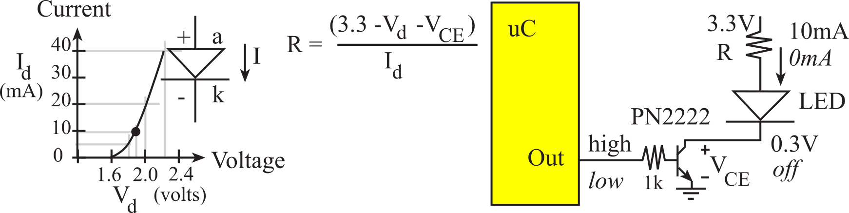
Figure 6.3.3. A BJT used to interface a light emitting diode.
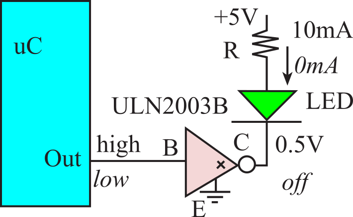
Figure 6.3.4. A Darlington transistor used to interface a light emitting diode.
: Assume VCE of the ULN2003B is 0.5V. What resistor value would you choose to operate the LED at 2V 10mA?
6.3.2. Metal-oxide-semiconductor field-effect transistor (MOSFET)
We will use the MOSFET as a voltage controlled switch, as shown in Figure 6.3.5. When the software outputs a high on the port, the MOSFET "turns on" and current flows from drain to source. When the software outputs a low on the port, the MOSFET "turns off" and no current flows from drain to source.
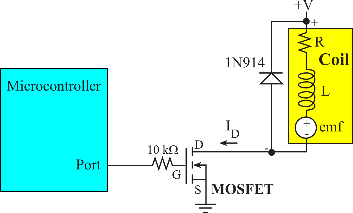
Figure 6.3.5. Simple MOSFET interface. IRLD024 data sheet.
The difficulty with interfacing most MOSFETs to a microcontroller is the large gate voltage needed to activate some MOSFETs. We will model inductive loads like speakers, motors, solenoids, and electromagnetic relays as the series combination of resistance, inductance and emf voltage. The resistance arises from the long copper wire, the inductance arises from the fact the wire is coiled, and the emf is a bidirectional coupling between electrical power and mechanical power. We will learn more about this model when interfacing motors in Section 8.3. Binary Actuators. The voltage across an inductor is
V = L dI/dt
We must either limit dI/dt or use a snubber diode like the 1N914 to remove the L*dI/dt.
Observation: When we use a transistor to turn current on and off, the dI/dt from on to off will be much higher than the dI/dt from off to on.
In this section, we will describe how to read a typical MOSFET data sheet. Figure 6.3.6 shows a saturation characteristic for an IRF540 MOSFET. Because the interface is a voltage-controlled switch, we define "fully activated" if the VDS voltage is close to 0, with current flowing through the load as needed. For Id less than 10 A (drain to source current) we need VGS (gate to source voltage) greater than 6V, and then the VDS (drain to source voltage) will be less than 0.8V. For a 10A 12V motor we define VGS less than 0.8V as "close to 0".
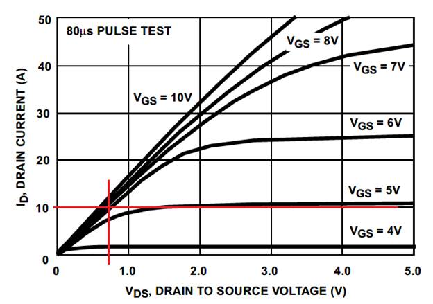
Figure 6.3.6. IRF540 MOSFET drain current versus drain to source voltage.
The goal is to choose a MOSFET to interface a device, as shown previously in Figure 6.3.5. The 10k resistor does not affect the voltage and current behavior of the interface, but does reduce the turn-on and turn-off times, reducing the back EMF generated in the inductive load.
Figure 6.3.7 presents simplified Id versus VDS curves for four different MOSFETs. The curves have a linear range, where Id increases with Vds. The curve will then have a saturated range where the current cannot be increased. The transition between linear and saturation depends on the gate voltage VGS. The first step in choosing a MOSFET is selecting the VGS to activate the voltage-controlled switch. If possible, we would like to interface a microcontroller output pin directly to the gate. In MOSFETs A and B, the 3.3V VOH of the digital output is not large enough to activate the MOSFET. Later in Section 8.xx (**add link**) we will use MOSFET circuits like like A and B to control DC motors. However, MOSFETs C and D will "fully activate" with a VGS of 3.3V. The second step in choosing a MOSFET is selecting one with ID large enough to operate the load. MOSFET C will have a VDS less the 0.1V for ID less than 2A. In contrast, MOSFET D can only operate with drain current less than 1 A.
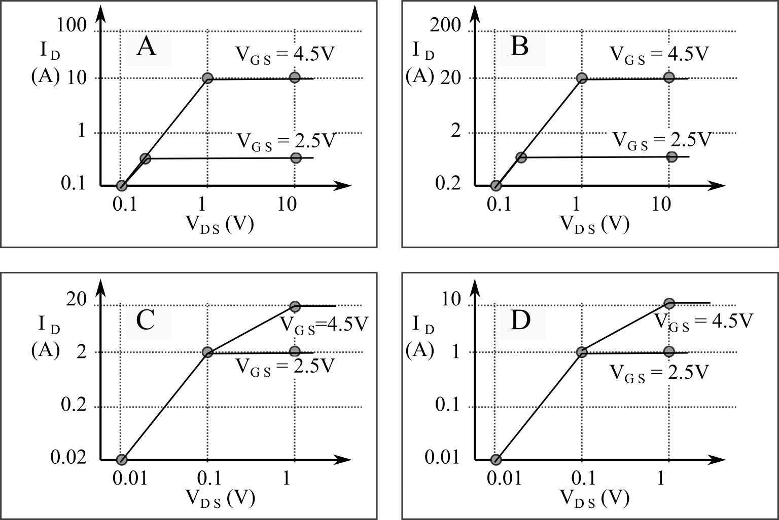
Figure 6.3.7. Simplified MOSFET curves.
Observation: It is good design to use a 2A MOSFET when solving a 1A problem. Conversely, operating a MOSFET at its maximum can cause reliability problems.
: Which MOSFET in Figure 6.3.7 would you use to interface a 1.5A load.
Sometimes we need to choose a MOSFET with a large VGS turn on voltage to achieve the desired drain current. The interfaces in Figure 6.3.8 use a PN2222 BJT in an inverting mode. The N-channel IRF540 requires a gate voltage above 7V to be fully active, therefore needs the BJT interface to boost the gate voltage. This IRF540 circuit is negative logic. When the port pin is high, the 2N2222 is active making the MOSFET gate voltage 0.3V (VCE of the PN2222). A VGS of 0.3V turns off the MOSFET. When the port pin is low, the 2N2222 is off making the MOSFET gate voltage +V (pulled up through the 10kΩ resistor). The VGS is +V, which turns the MOSFET on. The IRF540 N-channel MOSFET can source up to 28A when the source-gate voltage is above 7V. .
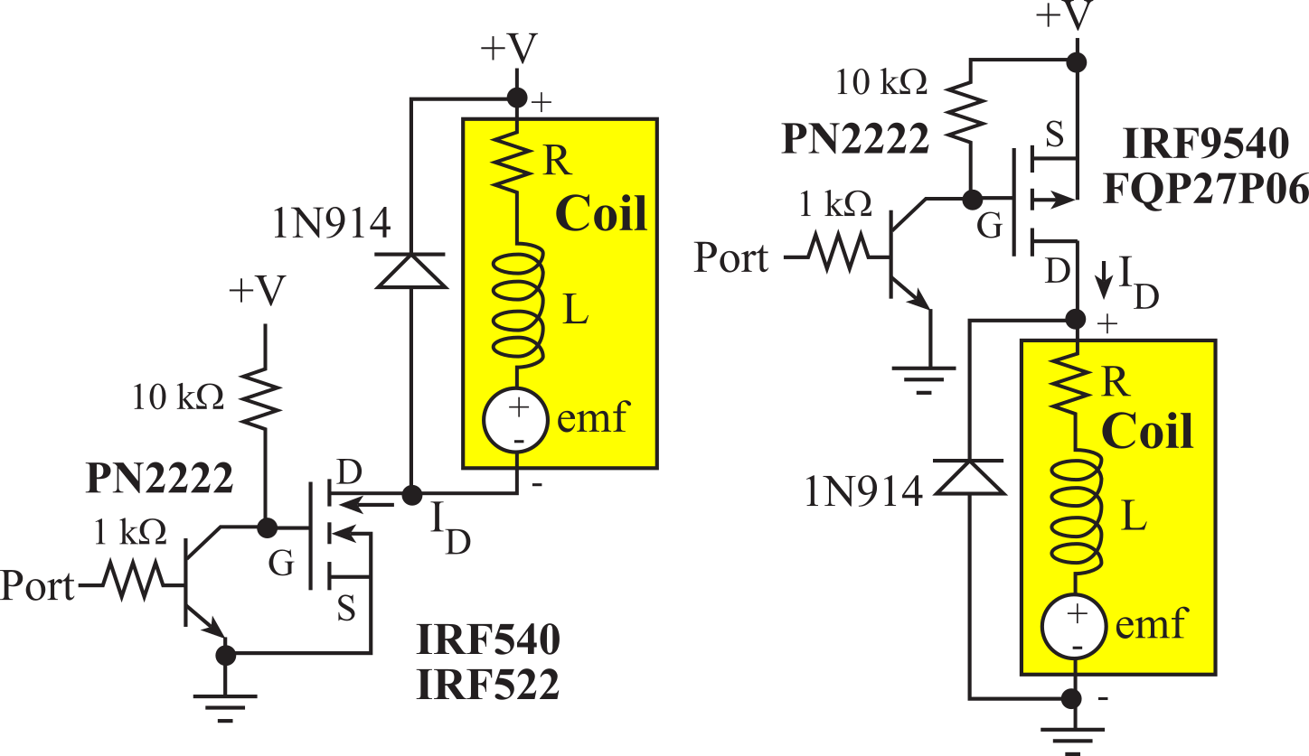
Figure 6.3.8. MOSFET interfaces with a large VGS turn on voltage. IRF540, IRF9540
The right side of Figure 6.3.8 shows a P-channel MOSFET interface. The IRF9540 P-channel MOSFET can source up to 20A when the source-gate voltage is above 7V. The FQP27P06 P-channel MOSFET can source up to 27A when the source-gate voltage is above 6V. This circuit is positive logic. When the port pin is high, the 2N2222 is active making the MOSFET gate voltage 0.3V. This makes VSG equal to +V-0.3, which turns on the MOSFET. When the port pin is low, the 2N2222 is off. Since the 2N2222 is off, the 10kΩ pull-up resistor makes the MOSFET gate voltage +V. In this case VSG equals 0, which turns off the MOSFET.
6.4. Analog Circuits
6.4.1. Operational Amplifier (op amp)
While the design of analog electronics is not an explicit objective of this book, we will include a brief discussion of analog circuit design issues often related to embedded systems. For example, low cost, small size, single voltage supply, and low power are four characteristics typical of embedded systems. Other factors to consider are reliability, noise, frequency response, availability, and temperature range.
Over a dozen manufacturers produce thousands of analog integrated circuits. Manufacturers include Analog Devices, Broadcom, Cirrus Logic, Infineon, Microchip, NXP Semiconductors, ON Semiconductor, Renesas, Skywork Solutions, ST Microchip, Texas Instruments, and Toshiba. The fact that there are so many op amps available makes the choice confusing. The manufacturers do publish a selection guide for their products to assist in finding an appropriate part from the ones they produce.
The op amp rails are its two power supplies, -Vs and +Vs. An op amp powered with ±12‑V rails operates properly when its inputs and outputs are between -10 to +10 V. A rail-to-rail op amp operates in a linear fashion for output voltages all the way from the minus rail to the plus rail. Some op amps operate "rail-to-rail" for both the inputs and output, while others operate "rail-to-rail" only for output.
Table 6.4.1 lists performance parameters of four op amps, and the choice of these devices typify the kinds of op amps used in an embedded system, but the selection of these four is not meant as a recommendation. Many op amps come in a variety of package sizes and are available in 1, 2, or 4 op amps per package. We will use rail-to-rail op amps to design analog circuits that run on a single +3.3 V supply. The OPA330 and MAX494 are low-power devices.
|
Single op amp Double op amp Quad op amp |
|
|
||
|
Description |
Low power |
Low power |
Medium speed |
High speed |
|
K, Open loop gain |
100 dB |
108 dB |
104 dB |
122 dB |
|
Rcm, Input impedance |
4 pF |
|
1012 Ω || 8pF |
1013 Ω || 6.5pF |
|
Rdiff, Input impedance |
2 pF |
2 MΩ |
1012 Ω || 8pF |
1013 Ω || 2.5pF |
|
Vos, Offset voltage |
50 µV |
0.5 mV |
3 mV |
0.5 mV |
|
Ios, Offset current |
500 pA |
6 nA |
100 pA |
10 pA |
|
Ib, Bias current |
1 nA |
60 nA |
100 pA |
10 pA |
|
en, Noise density |
55 nV/√Hz |
25 nV/√Hz |
50 nV/√Hz |
5 nV/√Hz |
|
f1, Gain*bandwidth product |
350 kHz |
500 kHz |
2.18 MHz |
38 MHz |
|
dV/dt, Slew rate |
0.16 V/µs |
0.2 V/µs |
3.6 V/µs |
22 V/µs |
|
+Vs, Voltage supply |
1.5 to 5.5 V |
2.7 to 6 V |
0 to 5 or ±5 V |
2.7 to 5.5 V |
|
Is, Supply current |
35 µA |
170 µA |
3 mA |
7.5 mA |
|
Cost (for dual version) |
$2 |
$12 |
$3 |
$6 |
Table 6.4.1. Parameters for various rail-to-rail CMOS op amps used in this chapter (with -Vs grounded). (2024 prices on www.mouser.com for quantity 1)
: What is the relationship between bandwidth and supply current?
Observation: The op amp should be much faster than the signal you are trying to process.
We will begin our discussion of op amps with the ideal op amp. For simple analog circuits using high quality devices, the ideal model will be sufficient. With an ideal op amp, the output voltage, Vout, is linearly related to the difference between the input voltages,
Vout = K * (Vy-Vx)
where the gain, K, is a very large number, as shown in Figure 6.4.1.
Voltage ranges of the inputs and outputs are bounded by the supply voltages, +Vs and -Vs. Op amp circuits found in many traditional analog design textbooks are powered with ±12-V supplies. On the other hand, it will reduce costs to power our embedded systems with a single voltage. More specifically, if the microcontroller operates with +3.3-V supply, we will run the analog circuits also on +3.3 V. We will use rail-to-rail op amps and set +Vs to +3.3 V and -Vs to ground.
No matter how we power the analog circuits, we assume the input and output voltages will exist between -Vs and +Vs. The input currents into the op amp are very small. Because the input impedance of the op amp is large, the ideal model assumes Ix and Iy are zero.
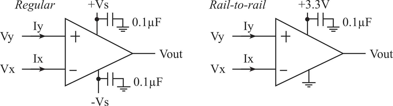
Figure 6.4.1. Regular op amp and a single supply rail-to-rail op amp.
If a feedback resistor is placed between the output and the negative terminal of the op amp, then this negative feedback will select an output such that Vx is very close to Vy. In the ideal model, we let Vx=Vy. One way to justify this behavior is to recall that Vout=K*(Vy-Vx). Since K is very large, the only way for Vout to be between -Vs and +Vs is for Vx to be very close to Vy.
We can design a threshold detector using positive or no feedback. A threshold detector has a binary output (true or false) depending on whether an input signal is greater than a threshold value. Positive feedback or no feedback drives Vout to equal -Vs or +Vs. If a feedback resistor is placed between the output and the positive terminal of the op amp, then this feedback will saturate the output to either the positive or negative supply. With no feedback, the output will also saturate. In both cases the output will saturate to the positive supply if Vy>Vx, and to the negative supply if Vx>Vy. Positive feedback can be used to create hysteresis.
Although the input impedance of an op amp is large, it is not infinite and some current enters the input terminals. Figure 6.4.2 illustrates the definition of input impedance. We define the common-mode input impedance, Rcm, as the common mode voltage divided by the common mode current. We define the differential input impedance, Rdiff as the differential voltage divided by the differential current. These parameters vary considerably from op amp to op amp. The CMOS and FET devices have very large input impedances.
The next realistic parameter we will define is open-loop output impedance. When the op amp is used without feedback, the op amp output impedance is defined as the open circuit voltage divided by the short circuit current. The output impedance is a measure of how much current the op amp can source or sink. The open loop output impedance of the TLC2274 is 140Ω.
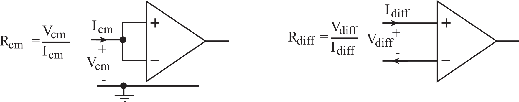
Figure 6.4.2. Definition of op amp input impedance.
: The MAX494 has an output short-circuit current of 30 mA. Assuming an output of 3.3 V, what is its output impedance?
As illustrated in Figure 6.4.3, the op amp offset voltage Vos is defined as the voltage difference between Vy and Vx which yields an output of zero. The offset current Ios is defined as the current difference between inputs. There will be an output error equal to the offset voltage times the gain of amplifier. Similarly, the offset current creates an offset voltage through the resistors of the circuit. Some op amps provide the capability to add an external potentiometer to nullify the two offset errors. The use of a null offset pot increases manufacturing costs and incurs labor costs to adjust it periodically. Therefore, the overall system cost may be reduced by using more expensive op amps that do not require a null offset pot. Alternatively, if the gain and offset are small enough not to saturate the output, then the offset error can be corrected in software by adding/subtracting an appropriate calibration constant.
The op amp bias current Ib is defined as the common current coming out of both Vy and Vx. We can reduce the effect of bias current by selecting resistors in our circuit to equalize the effective impedance to ground from the two input terminals.
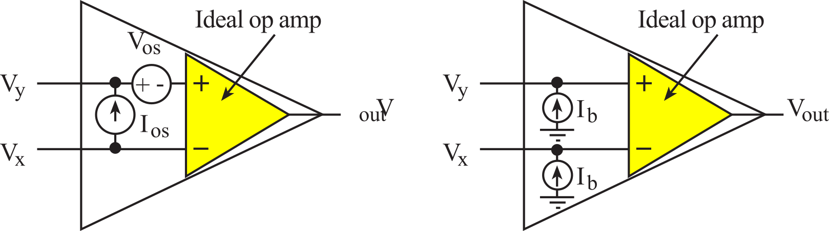
Figure 6.4.3. Definition of op amp offset voltage, offset current, and bias current.
: Consider the situation where a MAX494 is used to create an analog amplifier with gain 100. What will be the output error due to offset voltage?
: Why can't a TLC2274 is be used to create an amplifier with gain 1000?
The input voltage noise, Vn, arises from the thermal noise generated in the resistive components within the op amp. Due to the white-noise process, the magnitude of the noise is a function of the bandwidth (BW) of the analog circuit. This parameter varies quite a bit from op amp to op amp. To calculate the RMS amplitude of the input voltage noise, we need to calculate, Vn = en*√(BW). To reduce the effect of noise we can limit the bandwidth of the analog system using an analog low pass filter or buy a better op amp. The output voltage noise will be the input voltage noise multiplied by the gain of the circuit.
There are two approaches to defining the transient response of our analog circuits. In the frequency domain we can specify the frequency and phase response. In the time domain, we can specify the step response. For most simple analog circuits designed with op amps, the frequency response depends on the op amp performance and the analog circuit gain. If the unity-gain op amp frequency response is f1, then the frequency response at gain, G, will be f1/G. The bandwidth, BW, is defined as the frequency at which the gain (Vout/Vin) drops to 0.707 of the original. The voltage gain in decibels Gdb is related to the voltage gain in V/V. When Vout/Vin equals 0.707 (√½), the Gdb = -3 dB.

The output slew rate is the maximum slope that the output can generate. Slew rate is important if the circuit must response quickly to changes in input (e.g., a sensor detecting discrete events). Alternatively, bandwidth is important if the circuit is responding to a continuously changing input (e.g., audio and video).
: Consider the situation where a MAX494 is used to create an analog amplifier with a gain of 100. What will be the bandwidth of this circuit? Given this bandwidth, what will be the RMS output voltage noise?
When we consider the performance of a linear amplifier normally we specify the voltage gain, input impedance and output impedance. These three parameters can be lumped into a single parameter, Adb, called the power gain. Let Vin Rin be the inputs and Vout Rout be the outputs of our amplifier. The input and output powers are Pin=V2in/Rin and Pout=V2out/Rout respectively. Then the power gain in decibels has voltage gain and impedance components.

6.4.2. Linear Circuit Design
A wide range of analog circuits can be designed by following these simple design rules.
1. Choose quality components.
It is important to use op amps with good enough parameters. Similarly, we should use low tolerance resistors and capacitors. On the other hand, once the preliminary prototype has been built and tested, then we could create alternative designs with less expensive components. Because a working prototype exists, we can explore the cost/performance tradeoff.
2. Negative feedback is required to create a linear mode circuit.
As mentioned earlier, the negative feedback will produce a linear input/output response. We place a resistor between the negative input terminal and the output (Figure 6.4.4). A corollary to this is we almost never place a resistor between the positive input terminal and the output.
Figure 6.4.4. Negative feedback is created by placing a resistor between the - input and output.
3. Assume no current flows into the op amp inputs.
Since the input impedance of the op amp is large compared to the other resistances in the circuit, we can assume that Ix=Iy=0.
4. Assume negative feedback equalizes the op amp input voltages.
If the analog circuit is in linear mode with negative feedback, then we can assume Vx=Vy.
5. Choose resistor values in the 1 kΩ to 1 MΩ range.
To have the resistors in the circuit be much larger than the output impedance of the op amp and much smaller than the input impedance of the op amp, we choose resistors in the 1 kΩ to 1 MΩ range. If we can, it is better to restrict values to the 10 kΩ to 100 kΩ range. If we choose resistors below 1 kΩ, then the currents will increase. If the currents get too large the batteries will drain faster, and the op amp may not be able to source or sink enough current. As the resistors go above 1 MΩ, the white noise increases, the current errors (Ios Ib In) become more significant. In addition, low tolerance resistors are expensive in sizes above 2 MΩ.
6. The analog circuit bandwidth depends on the gain and the op amp performance.
Let the unity-gain op amp frequency response be f1, and let the analog circuit gain be G. The frequency response or bandwidth of the analog circuit, BW, will be f1/G. Design the circuit bandwidth 10 times faster than the signal you are trying to process.
7. Equalize effective resistance to ground at the two op amp input terminals.
To study the bias currents, consider all other voltage sources as shorts to ground, and all other current sources as open circuits. Adjust the resistance values in the circuit so that the impedance from the + terminal to ground is the same as the impedance from the - terminal to ground. In this way, the bias currents will create a common mode voltage, which will not appear at the op amp output because of the common mode rejection of the op amp.
8. The impedance is the voltage divided by the current.
If the analog circuit has a single input voltage, then the input impedance, Zin, is simply the input voltage divided by the input current as shown in the top of Figure 6.4.5. The output impedance, Zout, is the open circuit output voltage divided by the short circuit output current.
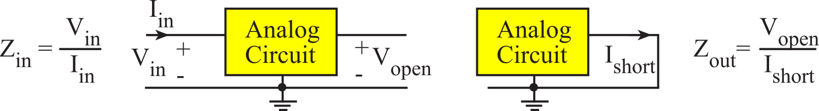
Figure 6.4.5. Definition of input and output impedance for an analog circuit with a single input.
If the input stage of the analog circuit is a differential amplifier with two input voltages, then we can specify the common mode input impedance, Zcm, and the differential mode input impedance, Zdiff. See Figure 6.4.6.
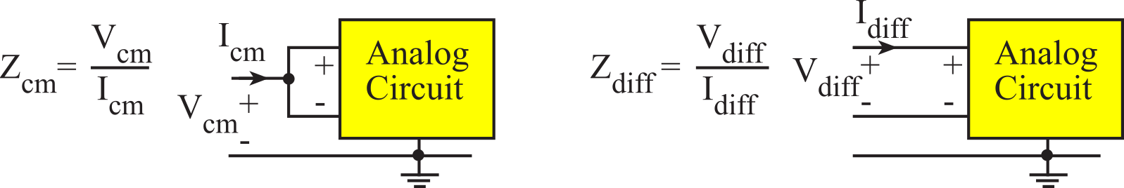
Figure 6.4.6. Definition of input impedance for an analog circuit with two inputs.
Observation: In most cases, the differential mode input impedance of the analog circuit will be the differential mode input impedance of the op amp.
9. Match input impedances to improve CMRR.
If the input stage of the analog circuit is a differential amplifier with two input voltages, a very important performance parameter is called the common mode rejection ratio (CMRR). It is assumed that the signal of interest is the differential voltage, whereas common mode voltages are considered noise. I.e., Vdiff will be the desired signal and Vcm is the added noise. The CMRR is defined to be the ratio of the differential gain divided by the common mode gain. See Figure 6.4.7. Therefore, a differential amplifier with a large CMRR will pass the signal and reject the noise. In decibels, it is calculated as
CMRR = 20 * log10 (Gdiff/Gcm)
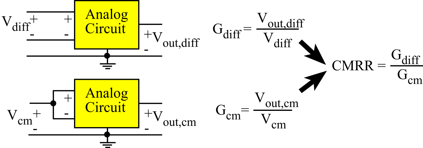
Figure 6.4.7. Definition of common mode rejection ratio (CMRR).
Remember, Vdiff is the signal and Vcm is noise. There are two sets of impedances we must match to achieve a good CMRR. Each amplifier input has a separate input impedance to ground, shown as Zin1 and Zin2 in Figure 6.4.8. To improve CMRR, we make Zin1 equal to Zin2. Similarly, the signal source (Vdiff) has a separate output impedance, Zout1 and Zout2. Again, we try to make Zout1 equal to Zout2. Unfortunately, if Zin1 does not equal Zin2 or if Zout1 does not equal Zout2 then a common mode signal (e.g., added noise in the cable) will appear as a differential signal to the analog circuit and thus be present in the output.
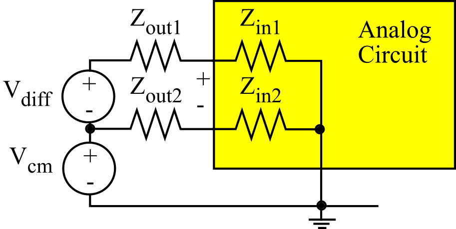
Figure 6.4.8. Circuit model for improving common mode rejection ratio (CMRR).
10. Rail-to-rail considerations.
When designing with rail-to-rail op amps, we must guarantee that the voltages at all input and output pins of the op amps never go outside the range of -Vs to +Vs .
Observation: Check the data sheet of your op amp. A OPA2350 powered with 0 to 3.3V operates in a linear fashion for outputs ranging from 0.05 to 3.25V. Conversely, a OPA4330 operates rail-to-rail for both inputs and outputs.
We will begin with an inverting amplifier (Figure 6.4.9), which is a simple linear mode analog circuit. The gain is the R2/R1 ratio. Notice that the gain response is independent of R3. Thus, we can choose R3 to be the parallel combination of R1||R2 so that the effect of the bias currents is reduced. Because Iy is zero, Vy is also zero. Because of negative feedback, Vx equals Vy. Thus, Vx equals zero too. Because Vx is zero, Iin is Vin/R1 and I2 is -Vout/R2. Because Ix is zero, Iin equals I2. Setting Iin equal to I2 yields
Vout = -(R2/R1)*Vin
The input impedance (Zin) of this circuit (defined as Vin/Iin) is R1. If the circuit were built with an OPA227, which has a gain bandwidth product of 8 MHz, the bandwidth of this circuit will be 8 MHz divided by the gain, R2/R1.

Figure 6.4.9. Inverting amplifier, built with OPA227, powered with +12 and -12V.
Common error: This low input impedance of Zin may cause loading on the previous analog stage.
Observation: The inverting amplifier input impedance is independent of the op amp input impedance.
The negative feedback will reduce the output impedance of the amplifier, Zout, to a value much less than the output impedance of the op amp itself, Rout. To calculate Zout, we first determine the open circuit voltage
Vopen = -(R2/R1)*Vin
We next determine the short circuit current, Ishort. This means we consider what would happen if the output were shorted to ground. If the output is shorted, the circuit is no longer in feedback mode, and Vx will not equal Vy. In fact, Vx will be a simple voltage divider from Vin through R1 and R2 to ground,
Vx = Vin*R2/(R1+R2)
Because of the large open-loop gain, the ideal output will attempt to become
Vo = K*(Vy-Vx) = -K*Vin*R2/(R1+R2)
The short circuit current will be a function of the ideal output voltage, and the output resistance of the op amp,
Ishort = Vo/Rout
The output impedance of the circuit is defined to be the open circuit voltage divided by the short circuit current, which for this inverting amplifier is
Zout = Vopen/Ishort = Rout*(R2+R1)/(K*R1)
Observation: The output impedance of analog circuits using op amps with negative feedback is typically in the mΩs.
6.4.3. Analog Reference
Some analog signals extend beyond the 0 to 3.3 V range of our microcontroller. Analog voltages above 3.3 V or below 0 V will damage the ADC on the microcontroller. One approach to allowing signed analog voltages, while still using a single voltage supply and protecting the microcontroller, is to create an analog ground that is at a different potential from digital ground. For our microcontroller systems, which are powered with a +3.3-V supply, we could create an analog ground that is at 1.5 V relative to the digital ground. Thus, analog signals ranging from -1.5 to +1.5 V are actually 0 to +3 V relative to the microcontroller digital ground. The first step to implementing this approach is to use an analog reference chip, like the ones shown in Table 6.4.2, to create a low-noise +1.50 V signal (the analog ground). The second step is to connect power to the analog circuits with -Vs set to digital ground, and the +Vs set to the +3.3 V supply. We will use rail-to-rail op amps that operate on 3.3-V power. The last step is to replace all connections to analog ground with the low-noise +1.50 V reference voltage. Figure 6.4.10 shows the inverting amplifier, redesigned from Figure 6.4.9 to operate on a single +3.3 V supply. The signals Vin and Vout are allowed to vary from 0 to +3 V relative to digital ground, but relative to the analog ground, these signals will vary from -1.5 to +1.5 V. An adjustable shunt voltage references like the LM4041 also can be used to create constant analog voltages. You can use this Excel sheet to design a voltage reference based on the LM4041, LM4041design.xlsx
|
Part |
Voltage (V) |
±Accuracy (mV) |
|
AD1580, AD589, REF1004, MAX6120, LT1034, LM4041C12 |
1.2 |
1 to 15 |
|
MAX6101, REF3312, ADR1581 |
1.25 |
2 |
|
MAX6108 |
1.6 |
3 |
|
ADR420, ADR520, REF191, MAX6191, LT1790, LM4120 |
2.048 |
1 to 10 |
|
AD580, REF03, REF1004, MAX6192, MAX6225, LT1389, LM336 |
2.5 |
1 to 75 |
|
AD1583, ADR530, ADR423, REF193, MAX6163, LT1461, LM4120 |
3 |
1.5 to 10 |
|
ADR366, REF196, MAX6331, LT1461, LM3411, LM4120 |
3.3 |
4 to 10 |
|
AD1584, ADR540, ADR292, REF198, MAX6241, LT1790, LM4040 |
4.096 |
2 to 8 |
Table 6.4.2. Parameters of various precision reference voltage chips.
Common Error: Precision reference chips do not provide much output current and should not be used to power other chips.
We can analyze the response of the circuit in Figure 6.4.9 by assuming an ideal op amp. Since there are no currents into the inputs, the voltage at the positive input will be 1.50 V. Because of negative feedback, the voltage at the negative input will also be 1.50 V. The current through R1 will be (Vin-1.5)/R1. The current through R2 will be (1.5-Vout)/R2. Since there are no currents into the inputs of the op amp, these two currents are equal,
(Vin - 1.5)/R1 = (1.5 - Vout)/R2
or Vout = 1.5 - (Vin - 1.5) R2/R1
Define the analog signals relative to 1.5V, i.e., V'in ≡ (Vin-1.5) and V'out ≡ (Vout-1.5). The circuit in Figure 6.4.9 implements a negative gain inverter.
V'out = - (R2/R1) V'in
Observation: It is important in this scheme to separate the digital and analog grounds avoiding direct connections between the two grounds.
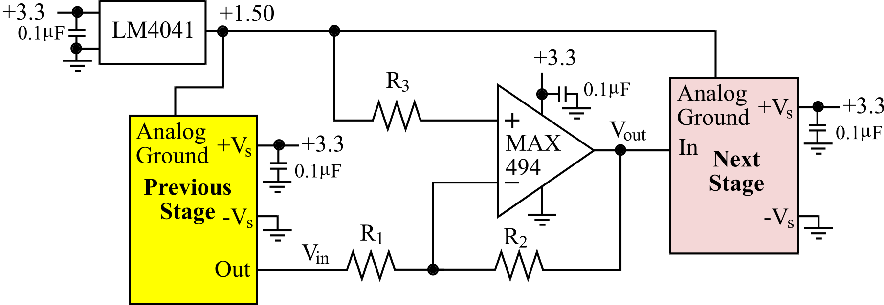
Figure 6.4.10. Inverting amplifier with an effective -1.5 V to +1.5 V analog signal range.
The next linear mode circuit we will study is the noninverting amplifier, as shown in Figure 6.4.11. The gain is 1+R2/R1. The noninverting amplifier cannot have a gain less than 1. Just like the inverting amp, the gain response is independent of R3. So, we choose R3 to be the parallel combination R1||R2 so that the effect of the bias currents is reduced.

Figure 6.4.11. Noninverting amplifier.
Because Iy is zero, Vy equals Vin. Because of negative feedback Vx equals Vy. Thus, Vx equals Vin too. Calculating currents we get, I1 is Vin/R1 and I2 is (Vout-Vin)/R2. Because Ix is zero, I1 equals I2. Setting I1 equal to I2 yields
Vout = (1 + R2/R1)*Vin
Using the simple op amp rules, Iy is zero, so the input impedance (Zin) of this circuit (defined as Vin/Iin) would be infinite. In this situation we specify the amplifier input impedance to be the op amp input impedance. If the circuit were built with an OPA350, which has a gain bandwidth product of 38 MHz, the bandwidth of this circuit will be 38 MHz divided by the gain.
: If the noninverting amplifier in Figure 6.4.11 were built with an OPA227, what would the input impedance of the amplifier be?
The calculation of the output impedance of this amp follows the same approach as the inverting amp,
Zout = Rout*(R2+R1)/(K*R1)
6.4.4. Build any linear analog circuit
The following design process can be used to build any linear analog circuit in the form of
Vout = A1V1 + A2V2 +...+AnVn + B
where A1 A2...An B are constants and V1 V2 ...Vn are input voltages. The circuit will be designed with one op amp beginning with the boiler plate shown in Figure 6.4.12.
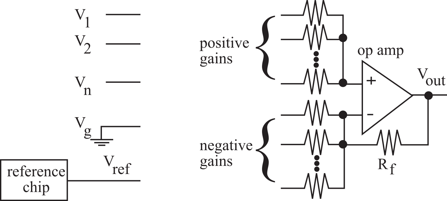
Figure 6.4.12. Boiler plate circuit model for linear circuit design.
The first step is to choose a reference voltage from available reference voltage chips, like ones shown in Table 6.4.2. The parameters to consider when choosing a voltage reference are voltage, package configuration, accuracy, temperature coefficient, and power. Let Vref be this reference voltage.
Common Error: If you use resistor divider from the power supply to create a voltage constant, then the power supply ripple will be added directly to your analog signal.
The second step is to rewrite the design equation in terms of the reference voltage, Vref. We make Aref = B/Vref.
Vout = A1V1 + A2V2 +...+AnVn + ArefVref
where A1 A2...An Aref are constants and V1 V2 ...Vn are input voltages. The third step is to add a ground input to the equation. Ground is zero volts (Vg=0), but it is necessary to add this ground so that the sum of all the gains is equal to one.
Vout = A1V1 + A2V2 +...+AnVn + ArefVref + AgVg
Choose Ag such that A1 + A2 +...+An + Aref + Ag = 1
In other words, let Ag = 1 - ( A1 + A2 +...+An + Aref )
The fourth step is to choose a feedback resistor, Rf, in the range of 10 kΩ to 1 MΩ. The larger the gains, the larger the value of Rf must be. Then calculate input resistors to create the desired gains. In particular,
|A1| = Rf / R1 so R1 = Rf / |A1|
|A2| = Rf / R2 so R2 = Rf / |A2|
|An| = Rf / Rn so Rn = Rf / |An|
|Aref| = Rf / Rref so Rref = Rf / |Aref|
|Ag| = Rf / Rg so Rg = Rf / |Ag|
Observation: We will get a low-cost solution if we choose standard resistor values, as shown in Section 7.5.
The last step is to build the circuit. If the gain is positive, then the input resistor is connected to the positive terminal of the op amp. Conversely, if the gain is negative, then the input resistor is connected to the negative terminal of the op amp. The feedback resistor, Rf, will always be connected from the negative input to the output.
Example 6.4.1. Design an analog circuit with two inputs and one output. The first input varies from 1 to 1.5 V and the second input varies from 0.75 to 1 V. The output will be equally sensitive to the two inputs, so the gain of the second input will be twice the gain of the first input. The output should range from 0 to 3 V. Build a circuit with a transfer function of Vout = 3V1 + 6V2 - 7.5.
Solution: The first step is to choose a reference voltage. The REF3312 +1.25-V voltage reference will be used. The second step is to rewrite the design equation in terms of the reference voltage. Notice that Aref = -7.5/1.25 = -6.
Vout = 3V1 + 6V2 - 6Vref
The third step is to add a ground input to the equation so that the sum of all the gains is equal to one. Notice, Ag = 1 - (3 + 6 - 6) = -2
Vout = 3V1 + 6V2 - 6Vref - 2Vg
The fourth step is to choose a feedback resistor, Rf =60 kΩ. This value is a common multiple of the gains: 6,3,2. Then calculate input resistors to create the desired gains.
R1 = Rf / 3 = 20 kΩ
R2 = Rf / 6 = 10 kΩ
Rref = Rf / 6 = 10 kΩ
Rg = Rf / 2 = 30 kΩ
The last step is to build the circuit, as shown in Figure 6.4.12. The positive gain inputs are connected to the plus input of the op amp and the negative gain inputs are connected to the minus input of the op amp input.
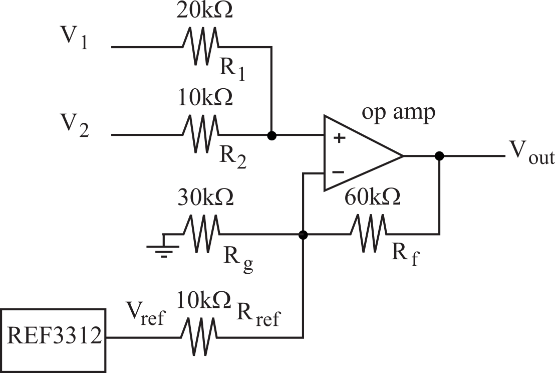
Figure 6.4.12. A linear op amp circuit.
Section 7.5 lists standard resistance values. When designing analog circuits, we need to select from these specific values to reduce cost and simplify manufacturing.
6.4.5. Instrumentation Amp
The instrumentation amp will amplify a differential voltage,
Vout = G*(V2-V1)
We should never use an instrumentation amp for a one-input, one-output analog circuit. For differential input circuits, we use instrumentation amps when one or more of the following conditions are true
a large gain (above 100),
a high input impedance, or
a good common mode rejection ratio.
To understand how an instrumentation amp works, see Figure 6.4.13. Because the inputs are connected to the plus terminal of op amps, both the common mode and differential mode input impedances will be large (ideally, no current flows into the op amp inputs). To allow for large gain, amplification occurs in two stages. The first stage has a gain of (1+2R2/R1), and the second stage has a gain of R4/R3. To achieve a large CMRR, the resistors must be tightly matched. In other words, R2 = R2, R3 = R3, R4 = R4.
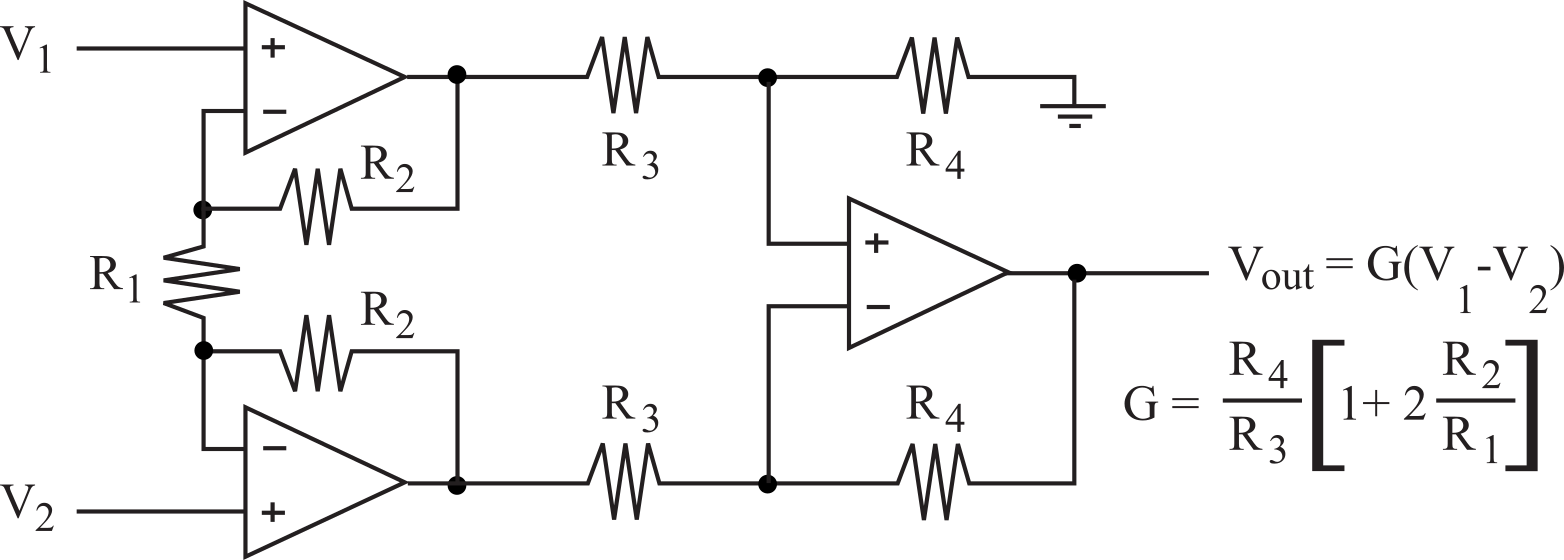
Figure 6.4.13. Instrumentation amplifier made with three op amps.
Observation: To achieve quality performance with a 3-op-amp instrumentation amp circuit, we must use precision resistors and quality op amps.
Common Error: If you use a potentiometer in place of one the gain resistors in the above circuit, then fluctuations in the potentiometer resistance that can occur with temperature, vibration, and time will have a strong effect on the amplifier gain.
Because matching resistors is expensive, we will never build an instrumentation circuit like 6.4.13, but rather, purchase an integrated solution. In other words, we can achieve higher performance at reduced cost by utilizing an integrated instrumentation amp. The gain is selected by external jumpers or external resistors. Many instrumentation amps are essentially Figure 6.4.13 with the R1 resistor existing externally. The MAX4460, AD627, and INA122 are single-supply rail-to-rail instrumentation amps. The AD627 and INA122 have the same pins and the same formula for calculating gain, as shown in Figure 6.4.14.
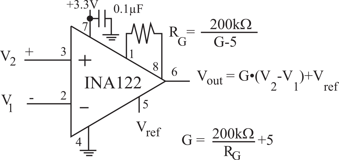
Figure 6.4.14. Integrated instrumentation amplifier made with INA122 or AD627.
: Assume R1 in Figure 6.4.13 equals RG in Figure 6.4.14. Find values of R2 R3 R4 to match the gain equations of the two circuits.
: What RG values would you select to have differential gains of 1, 5, 105?
Common Error: If you use a potentiometer as the RG gain resistors in the above circuit, then fluctuations in the potentiometer resistance that can occur with temperature, vibration, and time will have a strong effect on the amplifier gain.
6.4.6. Voltage Comparator
The open loop or saturated mode performance of a OPA2350 op amp can be studied by looking at the simple circuit in Figure 6.4.15. We use saturated mode to create a threshold detector. When the input, V1, is above the reference, Vt, then the output, V2, saturates to +3.3 V. Similarly, when V1 is below Vt then V2 saturates to 0 V.

Figure 6.4.15. A positive logic voltage comparator using an OPA2350 op amp.
The OPA2350 will operate on a supply range of 2.7 to 5.5 V. Notice that it will create a digital output when +Vs is 3.3V and -Vs is ground. The input voltages on input pins of the OPA2350 must be between -0.3 and +3.6V. The short circuit output current of the OPA2350 is 80 mA. The OPA2350 slew rate is 22V/µsec, with a settling time of 500ns.
We can use a voltage comparator to detect events in an analog waveform. The input voltage range is determined by the analog supply voltages of the comparator. The output takes on two values, shown as Vh and Vl in Figure 6.4.16. A comparator with hysteresis has two thresholds, Vt+ and Vt-. In both the positive and negative logic cases the threshold (Vt+ or Vt-) depends on the present value of the output.
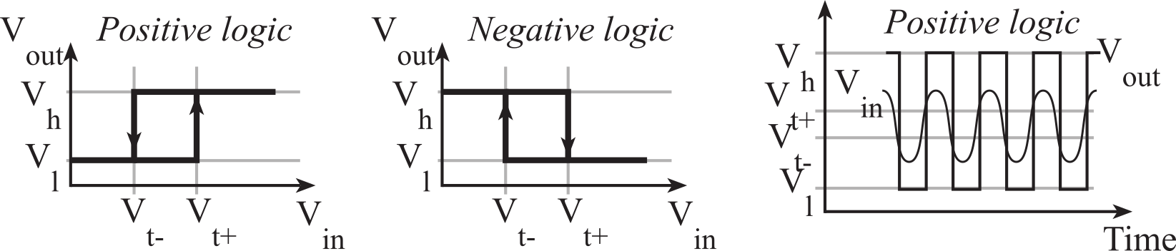
Figure 6.4.16. Input/output response of voltage converters with hysteresis.
Hysteresis prevents small noise spikes from creating a false trigger.
Performance Tip: To eliminate false triggering, we select a hysteresis level (Vt+ - Vt-) greater than the noise level in the signal.
In Figure 6.4.17, a rail-to-rail op amp is used to design a voltage comparator. Since the output swings from 0 to 3.3 V, it can be connected directly to an input pin of the microcontroller. On the other hand, since +3.3 and 0 are used to power the op amp, the analog input must remain in the 0 to +3.3 V range. The hysteresis level is determined by the amplitude of the output and the R1/(R1+R2) ratio. If the output is at 0V, the voltage at the +terminal is Vin*R2/(R1+R2). The output switches when the voltage at the +terminal goes above 1.65. By solving for Vin*200k/(10k+200k)=1.65, we see Vin must go above +1.73 for the output to switch. Similarly, if the output is at +3.3 V, the voltage at the +terminal can be calculated as Vin+(3.3-Vin)*R1/(R1+R2). The output switches back when the voltage at the +terminal goes below 1.65. By solving Vin+(3.3-Vin)*R1/(R1+R2)=1.65, we see Vin go below +1.57 before the +terminal of the op amp falls below 1.65 V. In linear mode circuits we should not use the supply voltage to create voltage references, but in a saturated mode circuit, power supply ripple will have little effect on the response.
Figure 6.4.17. A voltage comparator with hysteresis using a rail-to-rail op amp.
The problem with Figure 6.4.17 is its poor input impedance. The plus terminal will be at 1.65 V, so current will flow from Vin to 1.65V through the 10-kΩ resistor, making the input impedance on the order of 10 kΩ. If we reverse the polarity of the comparator, we can connect the input directly into an op amp terminal, resulting in an essentially infinite input impedance.
Figure 6.4.18. A better voltage comparator with hysteresis using a rail-to-rail op amp.
6.5. Analog Filters
6.5.1. Simple Analog Filters
We will use a low-pass filter to remove unwanted high frequency signals. Figure 6.5.1 shows a passive low pass filter. The impedance of a capacitor is 1/(jωC). At DC, the capacitor is open, and the gain is one. At AC, the gain is

The cutoff frequency is ω = 1(RC), or is fc = 1(2πRC)

Figure 6.5.1. A passive low pass filter using a resistor and capacitor.
We can add a capacitor in parallel with the feedback resistor in the inverting amplifier to create a simple one pole low-pass filter. The impedance of a resistor, R2 in parallel with the capacitor, C, is a function of frequency, see Figure 6.5.4.
![]()
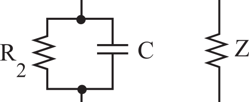
Figure 6.5.4. A parallel combination of a resistor and capacitor make a frequency-dependent impedance.
In Figure 6.5.5, the feedback path has both a resistor and capacitor. Therefore, the gain of the circuit is -Z/R1, which exhibits low-pass behavior. The cutoff frequency is defined to be the frequency at which the gain drops to 0.707 of its original value. In this simple low-pass filter, the cutoff frequency, fc, is 1/(2πR2C). The gain drops off at high frequencies.
Vout/Vin = (-R2/R1)*(1/(1+jωR2 C))
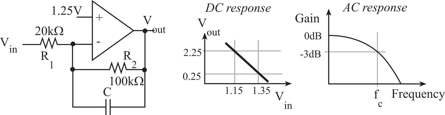
Figure 6.5.5. One pole low-pass analog filter.
We classify this low-pass filter as one pole, because the transfer function has only one pair of poles in the s-plane. One pole low-pass filters have a gain versus frequency response of
![]()
We will use a high-pass filter (HPF) to remove unwanted low frequency signals. Sound and biopotentials are examples of signals where the low frequency components are not wanted. If we place a capacitor in series, it will block low frequencies. One of the difficulties with high-pass filters for embedded systems is the fact that we often power analog electronics with a single supply. Because we cannot process negative voltages, we must use an analog ground different from the digital ground when building high-pass filters, as illustrated in Figure 6.5.6. The filter on the left is a simple approach. The middle one is low cost and not appropriate for high fidelity systems, because it uses the 3.3V directly. The one on the right is appropriate for differential signals. Each of these filters has a one-pole HPF shape, with 2πf=ω, and 1/fc=2πRC.
![]()
or
![]()
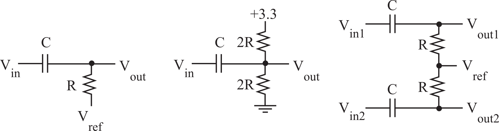
Figure 6.5.6. One pole high-pass analog filters operating on a single supply voltage.
6.5.2. Butterworth Filters
Higher order analog filters can be designed using multiple capacitors. One of the advantages of the two-pole Butterworth analog filter is that if the capacitors maintain the 2/1 ratio, the analog circuit will be a Butterworth filter. Figure 6.5.7 is a template for a Salen-Key form of the filter. The design steps for the two-pole Butterworth low-pass filter are as follows:
1) Select the cutoff frequency, fc
2) Divide the two capacitors by 2πfc (let C1A, C2A be the new capacitor values)
C1A = 141.4µF/2πfc
C2A = 70.7µF/2πfc
3) Locate two standard value capacitors (with the 2/1 ratio) with the same order of magnitude as the desired values. We can create capacitors with a 2/1 ratio using three capacitors of the same value. Let C1B, C2B be these standard value capacitors, let x be this convenience factor
C1B = C1A/x
C2B = C2A/x
4) Adjust the resistors to maintain the cutoff frequency
R = 10kΩ*x
5) Vref can be set to analog ground, e.g., 1.50V or 0V.
![]()
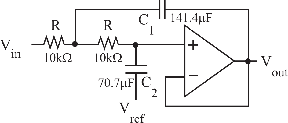
Figure 6.5.7. Two-pole Butterworth low-pass analog filter (download and open this lpf.xlsx spreadsheet file.
The analog filters in this section all require low leakage, high accuracy and low temperature coefficient capacitors like C0G ceramic.
Performance Tip: If you choose standard value resistors near the desired values, you will save money, and the circuit will still be a Butterworth filter. The only difference is that the cutoff frequency will be slightly off from the original specification.
We can use a similar approach to design a two-pole Butterworth high-pass filter. Figure 6.5.8 is a template for a Salen-Key form of the HPF. The design steps for the two-pole Butterworth high-pass filter are as follows:
1) Select the cutoff frequency, fc
2) Divide the two capacitors by 2πfc (let CA be the new capacitor values)
CA = 10µF/2πfc
3) Locate a standard value capacitor with the same order of magnitude as the desired value. Let CB, be this standard value, let x be this convenience factor
CB = CA/x
4) Adjust the two resistors to maintain the cutoff frequency
R1 = 70.7kΩ*x and R2 = 141.4kΩ*x
5) Vref should be set to analog ground, e.g., 1.50V.

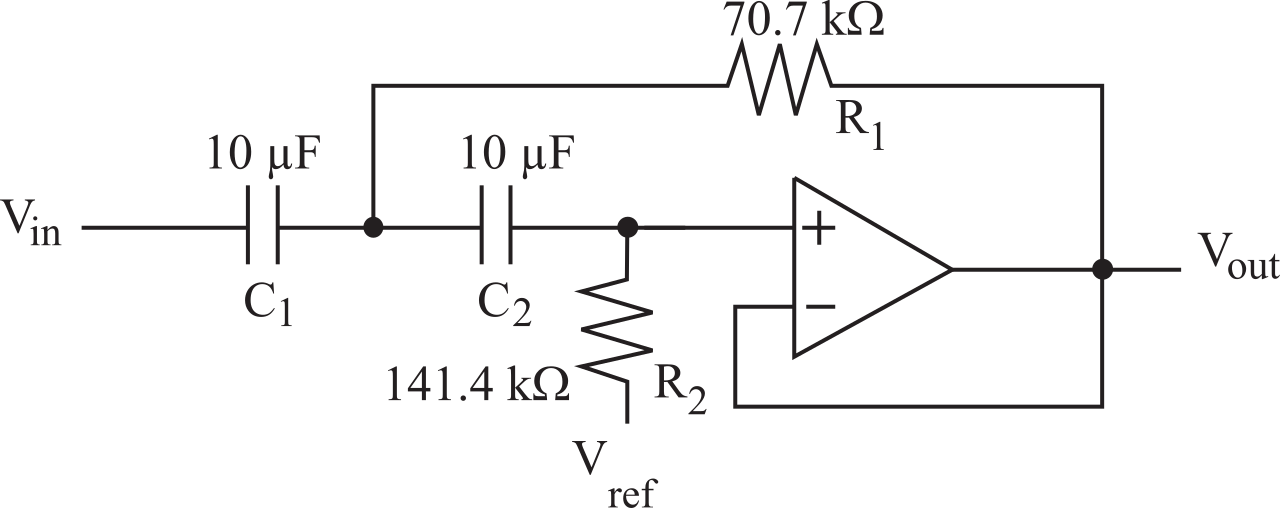
Figure 6.5.8. Two-pole Butterworth high-pass analog filter.
Webench is a free design tool from Texas Instruments you can use to design analog filters (https://www.ti.com/tool/WEBENCH-CIRCUIT-DESIGNER). Using these design tools, you will be able to create filters much better than the ones presented in this book.
6.6. Printed Circuit Board Layout and Enclosures
Begin with choosing a PCB size you need to hold all the components. Next you choose a box with which to enclose the system. The enclosure is an important aspect of the design. It determines the look and feel of the device. Many manufacturers give suggested PCB sizes for their enclosures. One way to make sure everything fits is to create a mockup. One collects all the electrical and mechanical components of the system. The PCB design is printed on paper and glued to cardboard or wood matching the thickness of the PCB. Mounting holes are drilled and components are attached to the PCB mockup. All components are assembled and mounted into the enclosure to verify proper fit. The left side of Figure 6.6.1 shows a mockup of an LM3S811-based recorder with an LCD touch screen. The right side shows the final system.
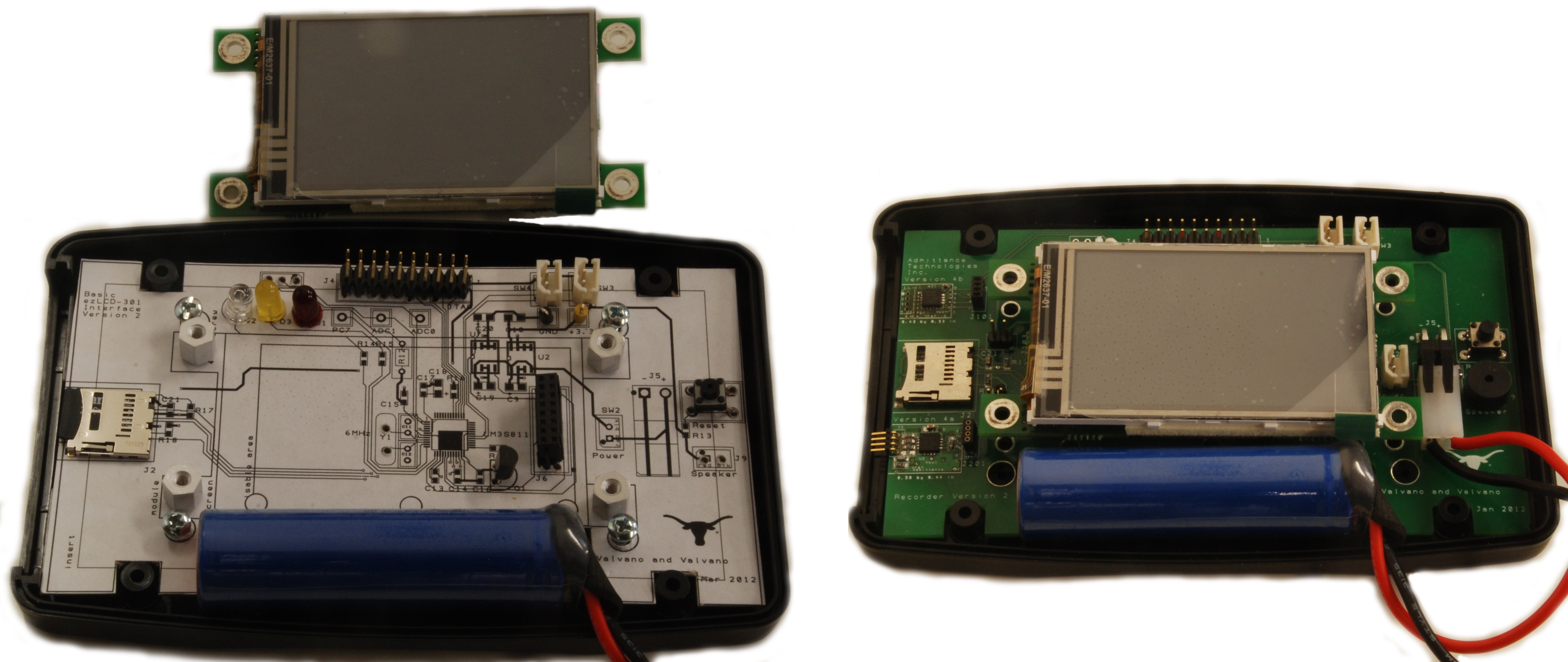
Figure 6.6.1. Mockup and PCB for an LM3S811 system using a PacTec enclosure.
Laying out a PCB is an art that is best learned by practice under the watchful eye of a master craftsman. So, show your PCB art to others and solicit feedback. For many years, it has been common PCB design practice to avoid 90° corners in PCB traces. Many claim that a 90° turn produces a ¼ turn inductor, which will affect the frequency response of the signals. The standard practice is to use a mitered corner replacing a 90° turn with two 45° turns. The reality is that the signal-integrity benefits of avoiding 90° angles are insignificant at the frequencies/edge-rates seen in microcontroller circuits (even up to and past 1 GHz/100ps). [Johnson, H and Graham, M, High-Speed Digital Design: a Handbook of Black Magic, Prentice Hall: New Jersey, 1993.] However, there are a few simple reasons to continue to avoid 90° angles. There is a higher possibility of an acid-trap forming during etching on the inside of the angle (especially in acute angles). An acid trap causes over-etching that can be a yield issue in PC boards with small trace widths. Routing at 45° typically reduces overall trace length and uses less board area. Most PCB designers think it looks better. Looking good is an important factor for anyone who appreciates the art of PCB layout.
This paragraph contains suggestions to consider when laying out a PCB. Make sure the "Snap to Grid" mode is active. You should experiment with different settings of the snap. A net defines which pins and pads must be connected. Just like software variables, nets should have descriptive names. You should visualize the unconnected nets while placing components on the board. Place all components initially on the board to facilitate input/output connectors. You also want to minimize the lengths and the crossings of the nets. Extra time spent placing components will be recovered many times over while the drawing the traces. Think about how it will be soldered, by placing though-hole components on the top side so soldering will occur on the bottom. Surface mount components can go on either side. Add top and bottom silk labeling to assist in construction, debugging, and device operation. For example, all components need labels (e.g., U1 R1 C1 J1 etc.), shown both on the board and the circuit diagram. Add test points at strategic points to assist in debugging. One inexpensive test point can be made by placing two holes 0.1 inch apart then soldering a U wire into it. You can also purchase test point hardware such as Keystone Electronics 5000 through 5004, which uses a 0.090 in pad with 0.043 in hole. One way to connect all traces is to go left-right on one side and up-down on the other side. Table 6.6.1 shows the trace width is a function of the length and current in the trace. 1oz/ft2 is a typical trace thickness.
|
Length |
Temperature Rise |
Current |
Thickness |
Resistance |
Trace Width |
|
5" |
1 C |
100 mA |
1 oz/ft2 |
1 Ω |
2 mil |
|
5" |
1 C |
200 mA |
1 oz/ft2 |
0.47 Ω |
5 mil |
|
5" |
1 C |
500 mA |
1 oz/ft2 |
0.13 Ω |
20 mil |
|
5" |
1 C |
1 A |
1 oz/ft2 |
0.05 Ω |
50 mil |
|
5" |
1 C |
2 A |
1 oz/ft2 |
0.02 Ω |
120 mil |
Table 6.6.1. Minimum trace width for various current levels
To verify all components will fit, you must analyze dimensions in 3-D. You can use a design tool like AutoCAD, or you can fabricate a mockup with actual parts. You can cut cardboard in the shape of the PCB, drill holes in the cardboard, and glue the parts onto the cardboard. Figure 6.6.2 shows an embedded system using an LM3S8962, placed in an enclosure.
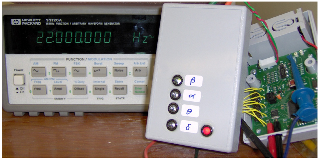
Figure 6.6.2. An EEG system designed with a LM3S8962 that fits into a case (designed by Katy Loeffler).
It is important to read data sheets and application notes for each component of the system. The manufacturer will suggest tips and reference designs for their parts. Figure 6.6.3 shows the suggested layouts for capacitors. The layouts show connections to power and ground on the microcontroller. It is recommended to place a capacitor as close to the chip as possible. The circles in Figure 6.6.3 represent vias to the power and ground planes. A) is the best practice because there is minimal inductance between capacitor, pins and power planes. B) is not recommended because the distance from pins to vias increases inductance in power rails. C) is acceptable because the distance from pin to via is short.
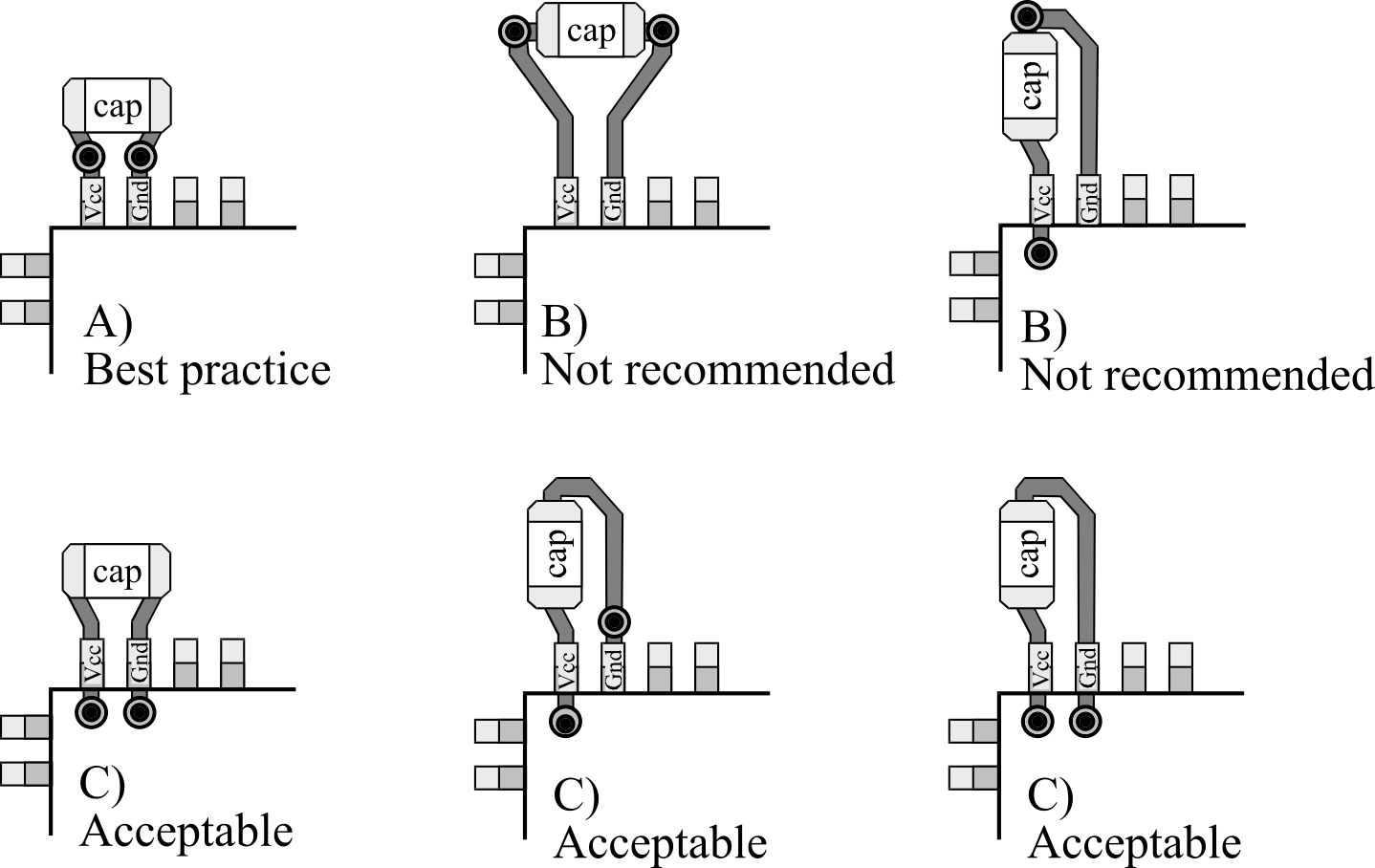
Figure 6.6.3. Capacitor layout suggestions (System Design Guidelines for Stellaris Microcontrollers, AN01283).
Figure 6.6.4 shows a suggested crystal layout, where an important objective is to minimize the effective capacitance from OSC0 to ground and from OSC1 to ground inherent in the board layout itself (called Cboard). When calculating the capacitor values needed for the oscillator one must account for this board capacitance. The values of these capacitors also depend on the crystal load capacitance, CL. A typical equation is C1 = C2 = 2×(CL - Cboard). This means one should not place power or ground planes under the crystal or the OSC0 and OSC1 signals.
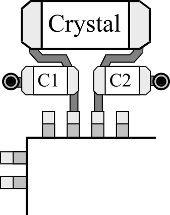
Figure 6.6.4. Crystal layout suggestion (System Design Guidelines for Stellaris Microcontrollers, AN01283).
Performance Tip: Look at the data sheet for your microcontroller and follow their recommended layout for power and crystal.
6.7. File systems
Many embedded systems need nonvolatile storage to save data. The first section presents the fundamental operation of flash memory. If we need small amounts of data storage, we can use the internal flash of the microcontroller, as shown in Section 6.7.2. Alternatively, if we need large amounts of data storage, we could interface a secure digital card (SDC), Section 6.7.3
6.7.1. Flash memory fundamentals
In general, we can divide memory into volatile and nonvolatile categories.
Volatile means it loses its data when power is removed and restored.
Nonvolatile means it retains its data when power is removed and restored.
There are many types of memory, but here are four of them
Volatile memory
- Static random access memory, SRAM
- Dynamic random access memory, DRAM
Nonvolatile memory
- Flash electrically erasable programmable read only memory, EEPROM
- Ferroelectric random access memory, FRAM
As you know data and the stack are allocated in RAM, because it needs read/write access.
DRAM has fewer transistors/bit compared to SRAM because it does require periodic refreshing.
Most Cortex M microcontrollers use SRAM because of its simple technology and ability to operate
on a wide range of bus frequencies. For random access memories, there is a size above which
DRAM is more cost effective than SRAM. Dynamic random access memory (DRAM) is the type of memory
found in most personal computers. Embedded devices like the Beaglebone and Raspberry Pi also use DRAM.
Ferroelectric RAM (FRAM) is a random access memory similar to DRAM but uses a ferroelectric layer instead of a dielectric layer. The ferroelectric layer provides the non-volatility needed for program storage. Some new lines of microcontrollers use FRAM instead of flash EEPROM for their non-volatile storage. The MSP430FRxx microcontrollers from Texas Instruments use FRAM to store programs and data in one shared memory object. Other companies that produce FRAM microcontrollers include Fujitsu and Silicon Labs. FRAM requires less power usage, has a faster write, and provides a greater maximum number of write-erase cycles when compared to flash. When compared to flash, FRAMs have lower storage densities, smaller sizes, and higher cost.
Solid-state disks can be made from any nonvolatile memory, such as battery-backed RAM, FRAM, or flash EEPROM. Personal computers typically use disks made with magnetic storage media and moving parts. While this magnetic-media technology is acceptable for the personal computer because of its large storage size (> 1 Tibibyte) and low cost (>$100 OEM), it is not appropriate for an embedded system because of its physical dimensions, electrical power requirements, noise, sensitivity to motion, and weight.
Secure digital (SD) cards use Flash EEPROM together with interface logic to read and write data. For an embedded system we could create a file system using an SD card or using the internal flash of the microcontroller itself. SD cards are an effective approach when file storage needs exceed 128 kibibytes, because of the low cost and simple synchronous serial interface. If we use the internal flash of the microcontroller itself, there will be no additional costs to developing this file system.
Smart phones, tablets, and cameras currently employ solid-state disks because of their small physical size and low power requirements. Unfortunately, solid-state disks have smaller storage sizes and higher cost/bit than the traditional magnetic storage disk. A typical 64-Gibibyte SD card costs less than $20. The cost/bit is therefore about $300/Tibibyte. In contrast, an 8-Tibibyte hard drive costs about $200 or $25/Tibibyte. The cost/bit of flash storage is expensive as compared to a traditional hard drive. However, there is a size point (e.g., below 128 Gibibyte), below which the overall cost of flash will be less than a traditional magnetic/motorized drive.
A flash memory cell uses two transistors; the gates of the two transistors are
positioned gate to gate separated by an insulation layer as shown in Figure 8.11.
Stacked Gate NMOS Transistor consists of
- Poly1 Floating Gate for charge storage
- Poly2 Control Gate for accessing the transistor
- Tunnel-oxide for Gate oxide
- Oxide-Nitride-Oxide (ONO) for the inter Poly Dielectric
- Source/Drain Junctions optimized for Program/Erase/Leakage
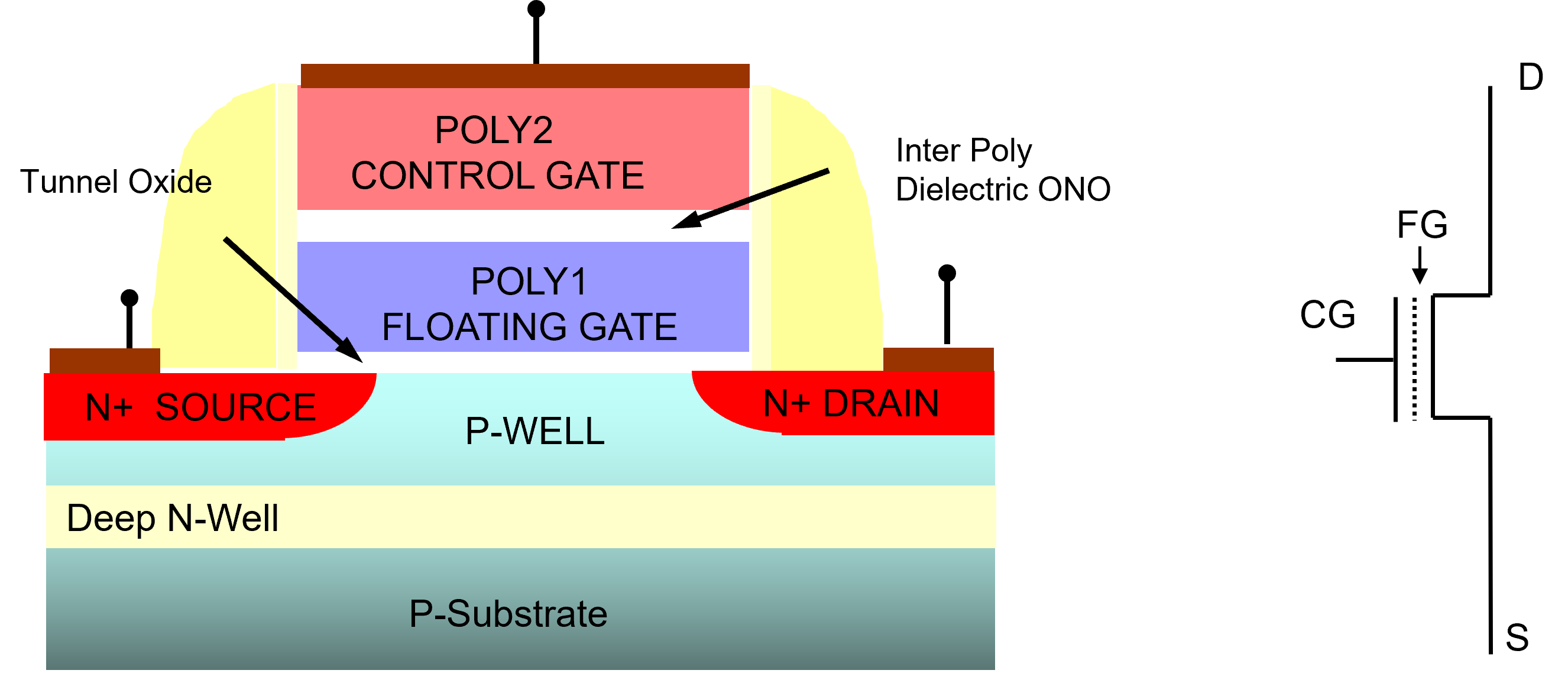
Figure 6.7.1. The floating gate in a flash memory cell creates the storage.
Figure 6.7.2 shows the basic operation of the flash cell. To erase a cell (making the data=1) electrons are removed from the FG = Low Vt To program a 0 into the cell, electrons are stored on the FG = High Vt. To read the contents, we sense the threshold Voltage shift = ΔQFG/CCG.

Figure 6.7.2. Basic operation of a flash memory cell.
Figure 6.7.3 shows the two of the most popular flash memory types. Both have Dual Gate NMOS with charge storage in Poly1 floating gate. The lack of contacts in NAND cell makes it inherently smaller in size.
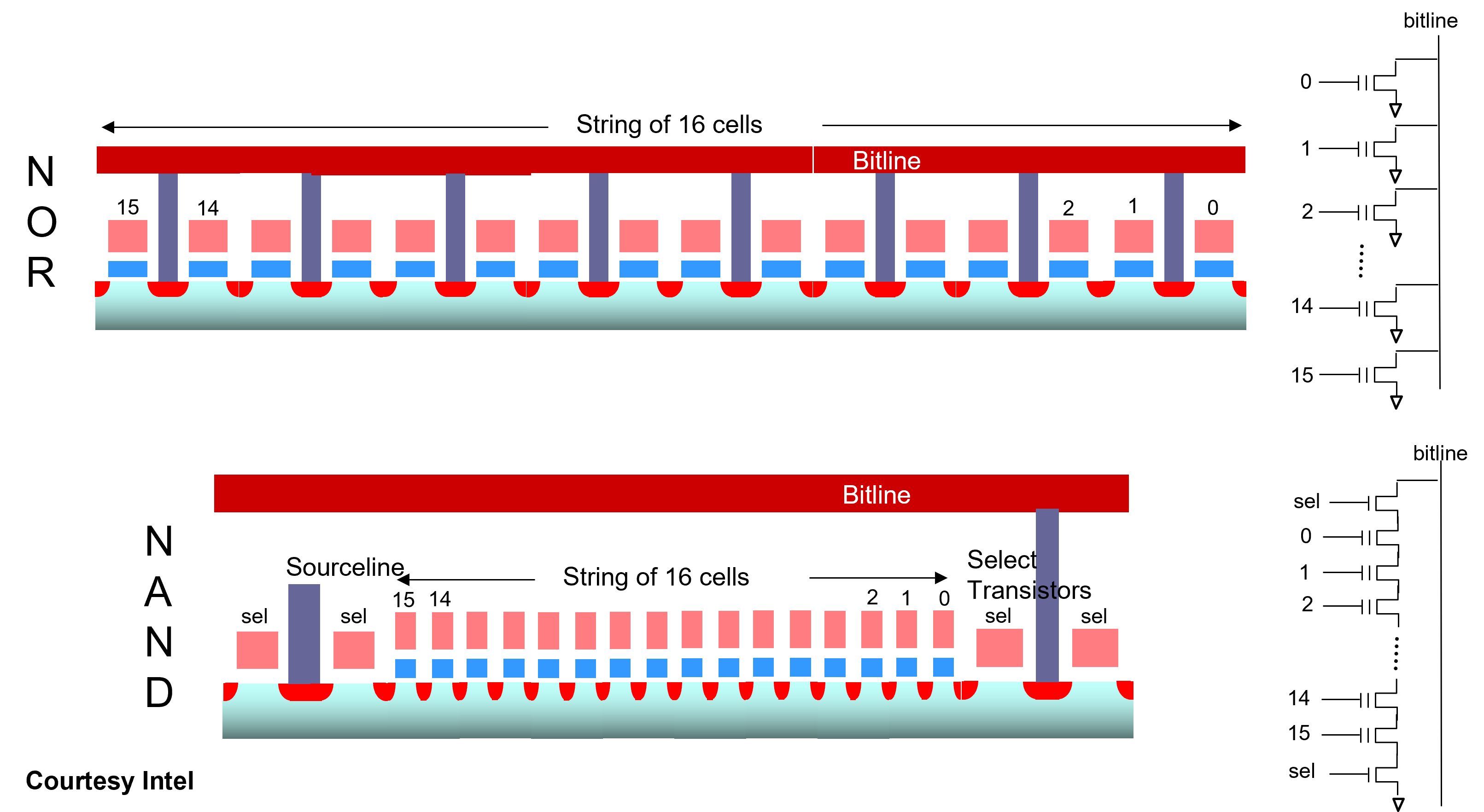
Figure 6.7.3. NAND and NOR flash architectures.
There are three operations we can perform on the cell. If we place a large voltage on the control gate (Vcg), we can get all the trapped charge to flow from the floating gate to the source below, hence erasing the cell, making its value equal to 1.
Conversely if we place a large voltage of the opposite polarity on the control gate, we can add charge to the floating gate, programming its value equal to 0. On the TM4C123 the smallest granularity with which we can erase is 1024 bytes. On the MSP432 we erase flash in blocks of 4096 bytes. However, we can program individual words on most flash memories including the TM4C123 and MSP432. Once erased to a 1 or programmed to a 0, the charge or lack of charge remains on the floating gate even if power is removed from the system. Hence, this memory is nonvolatile. Data in the TM4C123 and MSP432 flash memories will remain valid for 20 years, and the memory will operate up to 100,000 erase/program cycles. Erasing and programming operations take a very long time compared to writing static RAM (SRAM). For example, it takes 8 to 15 ms to erase an entire 1024-byte page on the TM4C123. In contrast, writing 256 words in RAM on an 80-MHz Cortex-M takes 5 cycles/loop, which adds up to 1280 cycles or 16 µs.
To read the value from flash, the control gate is activated. There is a threshold voltage for the control gate at which source-drain current (Id) flows if the bit is 0 and will not flow if the bit is 1. The threshold voltage is depicted as the dotted line in Figure 6.7.4.
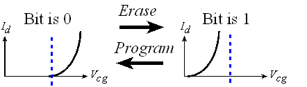
Figure 6.7.4. The trapped charge in the floating gate affects the relationship between control gate voltage and drain current.
For more information on flash, see http://computer.howstuffworks.com/flash-memory.htm. For information on RAM memory, see http://computer.howstuffworks.com/ram.htm. In summary:
- Flash memory cells have two transistors, so it is has very high density
- Nonvolatile behavior implemented as trapped/no charge on the floating gate
- We can erase an entire block (1k or 4k), making all bits 1
- We can program individual bytes/words, making bits 0 as needed
- Both erasing and programming are very slow compared to reading
6.7.2. Internal flash memory
One inexpensive approach to developing a file system is to use the internal flash storage of the microcontroller. The TM4C123 has 256 kibibytes of internal flash, existing from addresses 0 to 0x0003FFFF. The MSPM0G3507 has 128 kibibytes of internal flash, existing from addresses 0 to 0x0001FFFF. Normally, we use the internal flash to save the machine code of our software. However, in this section we will allocate half of the flash, which is 128 kibibytes, to create a solid state disk. We divide the disk into sectors and operate on a sector by sector basis. Typically, the sector size is a power of 2; let each sector be 2p bytes. This means we will partition the 217-byte disk into 2m sectors, where m+p=17. In general, there are three operations: we can erase (set bits to 1), program (set bits to 0), and read. The physical layer functions provide these basic operations. Program 6.7.1 shows the prototypes for the TM4C123. Implementations of these functions can be found on the starter files, see the project named Flash_4C123. We do not need physical layer functions to read the flash, because once erased and programmed, software simply reads from the memory address in the usual manner. The TM4C123 is optimized for programming up to 128-byte (32-word) aligned "mass writes" or "fast writes". The MSP432 implements this feature for up to 64-byte (16-word) arrays. The smallest block that we can erase on the TM4C123 is 1024 bytes. On the MSP432 we erase flash in blocks of 4096 bytes.
//------------Flash_Erase------------
// Erase 1 KB block of flash on TM4C123
// Input: addr 1-KB aligned flash memory address to erase
// Output: 0 if successful, 1 if fail
int Flash_Erase(uint32_t addr);
//------------Flash_Write------------
// Write 32-bit data to flash at given address.
// Input: addr 4-byte aligned flash memory address to write
// data 32-bit data
// Output: 0 if successful, 1 if fail
int Flash_Write(uint32_t addr, uint32_t data);
//------------Flash_WriteArray ------------
// Write an array of 32-bit data to flash starting at given address.
// Input: source pointer to array of 32-bit data
// addr 4-byte aligned flash memory address to start writing
// count number of 32-bit writes
// Output: number of successful writes; return value == count if ok
// Note: at 80 MHz, it takes 678 usec to write 10 words
int Flash_WriteArray(uint32_t *source, uint32_t addr, uint16_t count);
Program 6.7.1. Prototypes for the physical layer functions to manage the flash.
6.7.3. Secure digital card (SDC)
The Secure Digital Memory Card (SDC) is a popular standard for data storage in embedded systems. The SDC is an example of a high-speed I/O device, and normally we would interface the SDC using DMA synchronization. However, when interfacing to the TM4C/MSP432, we will use busy-wait synchronization with the understanding that peak bandwidth will be limited by software and not SDC performance. If we wished to improve performance, then DMA synchronization could be used. The SDC is upward-compatible to MULTI-MEDIA CARD (MMC) so that the SDC-compliant interfaces can also use an MMC with an appropriate adapter. There are also smaller versions, such as MINISD and MICROSD, where the differences are in the connector rather than the electrical specification. The card itself has a microcontroller in it. The flash memory operations, such as erasing, reading, and writing, are performed on this microcontroller. The data is transferred between the memory card and the host controller as 512-byte blocks. In this way, the SDC can be viewed like a generic hard disk drive. In other words, the low-level drivers perform block reads and writes. A 2-gibibyte SDC will have over 4 million (231/29) blocks, and the low-level driver will allow you to read or write any of these blocks. Program 8.3 shows a possible header file for such a low-level software interface. The implementation of this SDC driver can be found on the book web site as SDC_xxx. The file system, written as a higher level driver, will format and partition this storage in a logical manner. You can download from the internet full-functioning SDC drivers and FAT16 file system for most microcontrollers. The FAT16 file system will allow data exchange between the microcontroller and a personal computer. The FAT32 is defined for only high capacity (>= 4G) cards. However, this section will serve as an introduction providing the basic ideas and fundamental theories. The file systems described in the next section will be a lot simpler than FAT16. The SDC software driver is similar to the driver for the internal flash memory presented in the last section. The eDisk_Init function must be called once. eDisk_ReadBlock is used to read 512 bytes of data from the SDC into RAM. eDisk_WriteBlock is used to write 512 bytes of data from RAM into the SDC. The write block function will perform the two step operating of erasing and then programming.
//*************** eDisk_Init ***********
// Initialize the interface between microcontroller and the SD card
// Inputs: drive number (only drive 0 is supported)
// Outputs: status
// STA_NOINIT 0x01 Drive not initialized
// STA_NODISK 0x02 No medium in the drive
// STA_PROTECT 0x04 Write protected
// since this program initializes the disk, it must run with
// the disk periodic task operating
DSTATUS eDisk_Init(BYTE drive);
//*************** eDisk_ReadBlock ***********
// Read 1 block of 512 bytes from the SD card (write to RAM)
// Inputs: pointer to an empty RAM buffer
// sector number of SD card to read: 0,1,2,...
// Outputs: result
// RES_OK 0: Successful
// RES_ERROR 1: R/W Error
// RES_WRPRT 2: Write Protected
// RES_NOTRDY 3: Not Ready
// RES_PARERR 4: Invalid Parameter
DRESULT eDisk_ReadBlock (
BYTE *buff, // Pointer to the data buffer into which to store
DWORD sector); // sector number to read from
//*************** eDisk_WriteBlock ***********
// Write 1 block of 512 bytes of data to the SD card (read from RAM)
// Inputs: pointer to RAM buffer with information
// sector number of SD card to write: 0,1,2,...
// Outputs: result
// RES_OK 0: Successful
// RES_ERROR 1: R/W Error
// RES_WRPRT 2: Write Protected
// RES_NOTRDY 3: Not Ready
// RES_PARERR 4: Invalid Parameter
DRESULT eDisk_WriteBlock (
const BYTE *buff, // Pointer to the data to be written
DWORD sector); // sector number
Program 6.7.2. Header file for the SDC driver (SDC_4C123).
With a 32-bit sector number we could support disk up to 232*29 bytes or 2 tibibytes. Figure 6.7.5 shows the connector pin-out and interface. The SDC has 9 to 12 contact pads, including four pins that comprise the synchronous serial interface. MOSI MISO and Sclk are the usual SPI signals, and CS line can be implemented with any regular output pin. The three contacts are assigned for power supply. The SDC works at supply voltages from 2.7 to 3.6 V. The current consumption can reach up to 15 mA in standby and 50 mA during operation. Some SD card connectors provide an additional pin to let the software know whether or not a SDC is inserted into the slot.
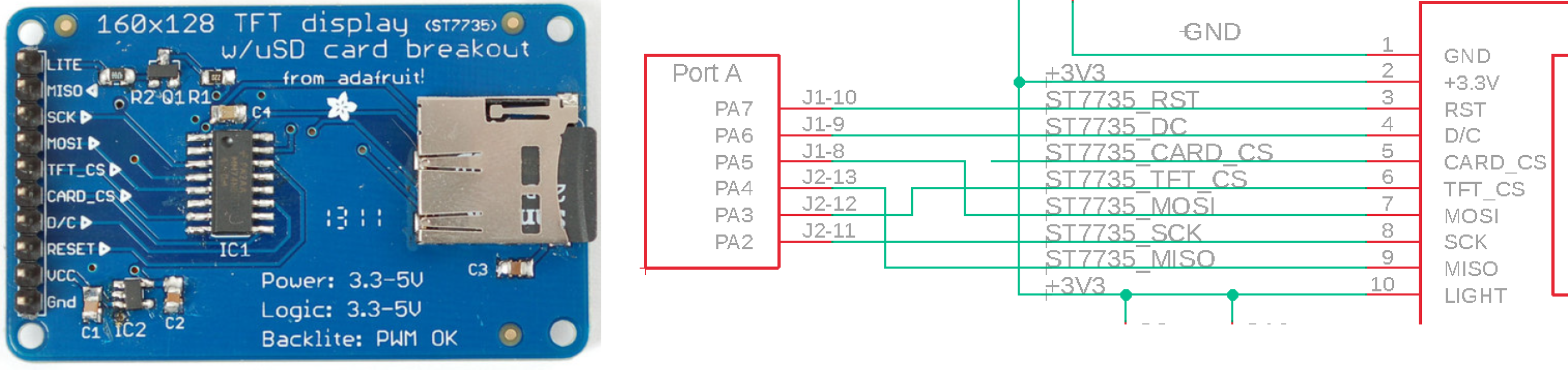
Figure 6.7.5. Connected the SDC on the ST7735R display. The SDC chip select can be either PD7 or PB0 (software compile flag).
There are three possible modes to interface the SD card: SD 4-bit mode, SD 1-bit mode, and SPI mode. The communication protocol for the SPI mode is simple compared to the native SD modes. Therefore, the SPI mode is suitable for low-cost embedded applications. In SPI mode, the pin 7 DO is always an output of the SDC, and pin 2 DI is always an input. Data are transferred in a byte-oriented synchronous serial fashion. The command frame from the microcontroller to the SDC is a fixed-length, six-byte packet shown in Figure 6.7.6. When a command frame is transmitted to the card, a response to the command (R1, R2, or R3) will eventually come from the card. The microcontroller must continue to send 0xFF frames to DI and receive frames from DO, until it receives a valid response. The command response time is 0 to 8 SPI frames (labeled as NCR in Figure 6.7.6). The CS signal must be held low during the entire transaction (command, response, and data transfer if exist). The 7-bit CRC field is optional in SPI mode, but it is required as a bit field to compose a command frame. The DI signal must be kept high during read transfer.

Figure 6.7.6. SDC command frame.
In SPI mode, data shift and data latch are done opposite clock edges respectively. There is an advantage that when shift and latch operations are separated, critical timing between two operations can be avoided. Therefore, timing consideration for IC design and board design can be relieved. The SD card uses CPOL=0, CPHA=0 mode as shown in Figure 6.7.7.

Figure 6.7.7. SPI CPOL=0, SPHA=0 mode.
There are many SD commands, some of which are shown in Table 6.7.1. For details on all commands, please refer to the SDA - SD Card Association at http://www.sdcard.org/. There are three command response formats: R1, R2, and R3, depending on the command index. Response R1 is 8 bits long and is returned for most commands. The R1 response has seven status bits, and a value of 0x00 means successful. Bit 6 is a parameter error, bit 5 is an address error, bit 4 is an erase sequence error, bit 3 is a communication CRC error, bit 2 is an illegal command, bit 1 is an erase reset, and bit 0 means the SDC is in the idle state. Most cards cannot change the block size, and it is fixed at 512 bytes
| Index | Argument | Response | Data | Description |
| 0 | None | R1 | No | Software reset |
| 1 or 41 | None | R1 | No | Initiate initialization process |
| 16 | Block length[31:0] | R1 | No | Change R/W block size |
| 17 | Address[31:0] | R1 | Yes | Read a block |
| 18 | Address[31:0] | R1 | Yes | Read multiple blocks |
| 24 | Address[31:0] | R1 | Yes | Write a block |
| 25 | Address[31:0] | R1 | Yes | Write multiple blocks |
| 58 | None | R3 | No | Read OCR |
Table 6.7.1. SD commands.
After power on reset, the SDC enters its native operating mode. To put the SDC in SPI mode, the following procedure must be performed. After the supply voltage reaches at least 2.2 V, wait at least one more millisecond. To initialize we need to set DI and CS high and send 74 or more clock pulses to Sclk. After this, the card will become ready to accept native commands. We set the SPI clock rate between 100 and 400 kHz and then send an Index=0 command with CS low to reset the card. The card samples the CS signal when an Index=0 command is received. If the CS signal is low, the card enters SPI mode. Since the Index=0 command must be sent as a native command, the CRC field must have a valid value. Once the card enters SPI mode, the CRC feature is disabled, and the CRC is not checked, so that the command transmission routine can be written with the hardcoded CRC value that is valid for only this command. When the Index=0 is accepted, the card will enter idle state and sends an R1 response with the idle bit (0x01).
In idle state, the card accepts only commands with index values of 0, 1, 41, and 58. Any other commands will be rejected. Command Index=58 allows you to check the working voltage range. Response R3 is an R1 plus information about the supply voltage. If the supply voltage is out of range, the card must be rejected. The card initiates initialization when a command with Index=41 is received. To poll end of the initialization, the host controller must repeatedly send commands with Index=41 until the idle bit goes low. When the card is initialized successfully, the idle bit in the R1 response is cleared. That is, the R1 response will change from 0x01 to 0x00. The initialization process can take hundreds of milliseconds and large cards make take longer. After the idle bit is cleared, read/write commands can be sent. Command Index=41 is recommended instead of Index=1 for SDC. Index=1 initiation can be tried if Index=41 is rejected. After initialization, the SPI clock rate can be increased to optimize the read/write performance. Most SD cards can handle SPI rates of 25 MHz. The speed will be dominated by software transferring data with the SPI port. To achieve higher bandwidth, you could use a DMA interface available on many high-performance microcontrollers.

Figure 6.7.8. SD data packets.
In a transaction with data transfer, one or more data packets will be sent/received after command response. See Figure 6.7.9. The data block is transferred as a data packet that consists of Token, Data Block, and CRC. The token for command indices 17, 18, and 24 is $FE. The token for command index 25 is $FC. A logic analyzer trace for a single-block read is shown in Figure 8.16. The resolution on the plot is not enough to see all the Sclk pulses. However, we see the CS line (labeled PA4 SS) goes low and remains low for the entire transaction. The microcontroller begins by sending an Index=17 read block command. The argument for this command will be the sector address from which to read. The command response will be R1 with a value of 0x00, which means okay. Next, the microcontroller sends many frames (300 µs on this system) waiting for the SDC. The last half of the transfer is a data packet being sent from the SDC to the microcontroller containing the 512 bytes read from that sector. On this system, it took 535 µs to read one block. If any error occurred during the read operation, an error token will be returned instead of data packet.
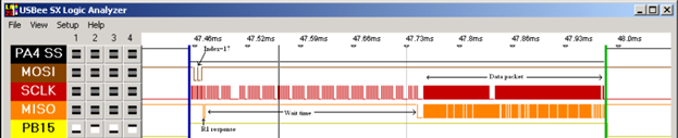
Figure 6.7.9. Single block read packet.
To write a block, the controller sends a write command. If the response R1 is 0x00, the microcontroller sends a data packet to the card after an eight-clock pause. The write data packet has the same format as read data packet. The CRC field can have any value unless the CRC function is enabled. When a data packet has been sent, the card responds a Data Response immediately following the data packet.
On top of the low-level ability to read and write blocks, we can build a file system. There is a simple FAT16 file system implemented in the project SDCFile_4C123. The interface in Figure 6.7.5 has two chip select signals. PA2 is used to select the ST7735R. Either PD7 or PB0 can be used to select the SDC. This implementation shares the SPI with the ST7735R display, meaning one must be careful not to mix file system operations with graphics output. Program 6.7.3 shows some of the header file ff.h.
FRESULT f_open (FIL* fp, const TCHAR* path, BYTE mode); /* Open or create a file */
FRESULT f_close (FIL* fp); /* Close an open file object */
FRESULT f_read (FIL* fp, void* buff, UINT btr, UINT* br); /* Read data from a file */
FRESULT f_write (FIL* fp, const void* buff, UINT btw, UINT* bw); /* Write data to a file */
FRESULT f_forward (FIL* fp, UINT(*func)(const BYTE*,UINT), UINT btf, UINT* bf); /* Forward data to the stream */
FRESULT f_lseek (FIL* fp, DWORD ofs); /* Move file pointer of a file object */
FRESULT f_truncate (FIL* fp); /* Truncate file */
FRESULT f_sync (FIL* fp); /* Flush cached data of a writing file */
FRESULT f_opendir (DIR* dp, const TCHAR* path); /* Open a directory */
FRESULT f_closedir (DIR* dp); /* Close an open directory */
FRESULT f_readdir (DIR* dp, FILINFO* fno); /* Read a directory item */
FRESULT f_mkdir (const TCHAR* path); /* Create a sub directory */
FRESULT f_unlink (const TCHAR* path); /* Delete an existing file or directory */
FRESULT f_rename (const TCHAR* path_old, const TCHAR* path_new); /* Rename/Move a file or directory */
FRESULT f_stat (const TCHAR* path, FILINFO* fno); /* Get file status */
FRESULT f_chmod (const TCHAR* path, BYTE value, BYTE mask); /* Change attribute of the file/dir */
FRESULT f_utime (const TCHAR* path, const FILINFO* fno); /* Change times-tamp of the file/dir */
FRESULT f_chdir (const TCHAR* path); /* Change current directory */
FRESULT f_chdrive (const TCHAR* path); /* Change current drive */
FRESULT f_getcwd (TCHAR* buff, UINT len); /* Get current directory */
FRESULT f_getfree (const TCHAR* path, DWORD* nclst, FATFS** fatfs); /* Get number of free clusters on the drive */
FRESULT f_getlabel (const TCHAR* path, TCHAR* label, DWORD* vsn); /* Get volume label */
FRESULT f_setlabel (const TCHAR* label); /* Set volume label */
FRESULT f_mount (FATFS* fs, const TCHAR* path, BYTE opt); /* Mount/Unmount a logical drive */
FRESULT f_mkfs (const TCHAR* path, BYTE sfd, UINT au); /* Create a file system on the volume */
FRESULT f_fdisk (BYTE pdrv, const DWORD szt[], void* work); /* Divide a physical drive into some partitions */
int f_putc (TCHAR c, FIL* fp); /* Put a character to the file */
int f_puts (const TCHAR* str, FIL* cp); /* Put a string to the file */
int f_printf (FIL* fp, const TCHAR* str, ...); /* Put a formatted string to the file */
TCHAR* f_gets (TCHAR* buff, int len, FIL* fp); /* Get a string from the file */
Program 6.7.3. Header file for a FAT16 file system (SDCFile_4C123).
Program 6.7.4 shows an example usage of the file system involving file reading and writing.
static FATFS g_sFatFs;
FIL Handle,Handle2;
FRESULT MountFresult;
FRESULT Fresult;
const char inFilename[] = "test.txt"; // 8 characters or fewer
void ReadExample(void){uint32_t successfulreads,count=0; char c;
Fresult = f_open(&Handle, inFilename, FA_READ);
if(Fresult == FR_OK){
// get a character in 'c' and the number of successful reads in 'successfulreads'
Fresult = f_read(&Handle, &c, 1, &successfulreads);
while((Fresult == FR_OK) && (successfulreads == 1)){
count++;
Fresult = f_read(&Handle, &c, 1, &successfulreads);
}
// close the file
Fresult = f_close(&Handle);
}
return count;
}
const char outFilename[] = "out.txt"; // 8 characters or fewer
void WriteExample(void){uint32_t successfulwrites;
// open the file to be written
// Options:
// FA_CREATE_NEW - Creates a new file, only if it does not already exist. If file already exists, the function fails.
// FA_CREATE_ALWAYS - Creates a new file, always. If file already exists, it is over-written.
// FA_OPEN_ALWAYS - Opens a file, always. If file does not exist, the function creates a file.
// FA_OPEN_EXISTING - Opens a file, only if it exists. If the file does not exist, the function fails.
Fresult = f_open(&Handle, outFilename, FA_WRITE|FA_OPEN_ALWAYS);
if(Fresult == FR_OK){
// jump to the end of the file
Fresult = f_lseek(&Handle, Handle.fsize);
// write a message and get the number of successful writes in 'successfulwrites'
Fresult = f_write(&Handle, "Another successful write.\r\n", 27, &successfulwrites);
Fresult = f_close(&Handle);
}
}
int main(void){
PLL_Init(Bus80MHz); // 80 MHz
ST7735_InitR(INITR_REDTAB); // shared with SDC
ST7735_FillScreen(0); // set screen to black
EnableInterrupts();
MountFresult = f_mount(&g_sFatFs, "", 0);
if(MountFresult){
while(1){}; // error
}
ReadExample();
WriteExample();
while(1){};
}
Program 6.7.4. Example usage of a file system (SDCFile_4C123).
6.8. Lab 6
Lab 6 for this course can be downloaded from this link Lab06.docx
Each lab also has a report Lab06Report.docx
This work is based on the course ECE445L
taught at the University of Texas at Austin. This course was developed by Jonathan Valvano, Mark McDermott, and Bill Bard.
Reprinted with approval from Embedded Systems: Real-Time Interfacing to ARM Cortex-M Microcontrollers, ISBN-13: 978-1463590154

Embedded Systems: Real-Time Interfacing to ARM Cortex-M Microcontrollers by Jonathan Valvano is
licensed under a Creative
Commons
Attribution-NonCommercial-NoDerivatives 4.0 International License.