Embedded Systems - Shape The World
Jonathan Valvano and Ramesh Yerraballi
Reprinted with approval from Embedded Systems: Introduction to ARM Cortex-M Microcontrollers, 2013, ISBN: 978-1477508992. For more information about the textbook see http://users.ece.utexas.edu/~valvano/arm/outline1.htm
1. General Information
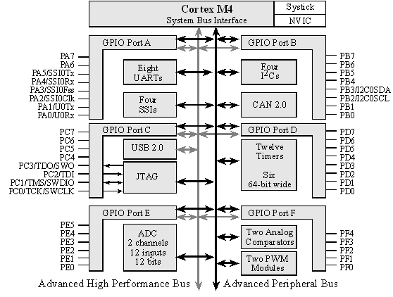
Figure 1.1. I/O port pins for the LM4F120H5QR / TM4C123GH6PM microcontrollers.
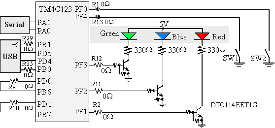
Figure 1.2. Switch and LED interfaces on the Tiva® LaunchPad Evaluation Board. The zero ohm resistors can be removed so the corresponding pin can be used for its regular purpose.
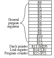
Figure 1.3. Cortex M registers.
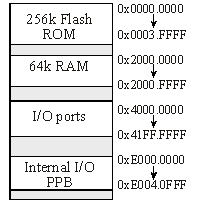
Figure 1.4. TM4C123/LM4F120 address map.
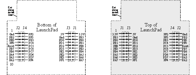
Figure 1.5. Pin locations on the LaunchPad.
2. Parallel Ports
|
Address |
7 |
6 |
5 |
4 |
3 |
2 |
1 |
0 |
Name |
|
$400F.E108 |
|
|
GPIOF |
GPIOE |
GPIOD |
GPIOC |
GPIOB |
GPIOA |
SYSCTL_RCGC2_R |
|
$4000.43FC |
DATA |
DATA |
DATA |
DATA |
DATA |
DATA |
DATA |
DATA |
GPIO_PORTA_DATA_R |
|
$4000.4400 |
DIR |
DIR |
DIR |
DIR |
DIR |
DIR |
DIR |
DIR |
GPIO_PORTA_DIR_R |
|
$4000.4420 |
SEL |
SEL |
SEL |
SEL |
SEL |
SEL |
SEL |
SEL |
GPIO_PORTA_AFSEL_R |
|
$4000.4510 |
PUE |
PUE |
PUE |
PUE |
PUE |
PUE |
PUE |
PUE |
GPIO_PORTA_PUR_R |
|
$4000.451C |
DEN |
DEN |
DEN |
DEN |
DEN |
DEN |
DEN |
DEN |
GPIO_PORTA_DEN_R |
|
$4000.4524 |
1 |
1 |
1 |
1 |
1 |
1 |
1 |
1 |
GPIO_PORTA_CR_R |
|
$4000.4528 |
0 |
0 |
0 |
0 |
0 |
0 |
0 |
0 |
GPIO_PORTA_AMSEL_R |
|
$4000.53FC |
DATA |
DATA |
DATA |
DATA |
DATA |
DATA |
DATA |
DATA |
GPIO_PORTB_DATA_R |
|
$4000.5400 |
DIR |
DIR |
DIR |
DIR |
DIR |
DIR |
DIR |
DIR |
GPIO_PORTB_DIR_R |
|
$4000.5420 |
SEL |
SEL |
SEL |
SEL |
SEL |
SEL |
SEL |
SEL |
GPIO_PORTB_AFSEL_R |
|
$4000.5510 |
PUE |
PUE |
PUE |
PUE |
PUE |
PUE |
PUE |
PUE |
GPIO_PORTB_PUR_R |
|
$4000.551C |
DEN |
DEN |
DEN |
DEN |
DEN |
DEN |
DEN |
DEN |
GPIO_PORTB_DEN_R |
|
$4000.5524 |
1 |
1 |
1 |
1 |
1 |
1 |
1 |
1 |
GPIO_PORTB_CR_R |
|
$4000.5528 |
0 |
0 |
AMSEL |
AMSEL |
0 |
0 |
0 |
0 |
GPIO_PORTB_AMSEL_R |
|
$4000.63FC |
DATA |
DATA |
DATA |
DATA |
JTAG |
JTAG |
JTAG |
JTAG |
GPIO_PORTC_DATA_R |
|
$4000.6400 |
DIR |
DIR |
DIR |
DIR |
JTAG |
JTAG |
JTAG |
JTAG |
GPIO_PORTC_DIR_R |
|
$4000.6420 |
SEL |
SEL |
SEL |
SEL |
JTAG |
JTAG |
JTAG |
JTAG |
GPIO_PORTC_AFSEL_R |
|
$4000.6510 |
PUE |
PUE |
PUE |
PUE |
JTAG |
JTAG |
JTAG |
JTAG |
GPIO_PORTC_PUR_R |
|
$4000.651C |
DEN |
DEN |
DEN |
DEN |
JTAG |
JTAG |
JTAG |
JTAG |
GPIO_PORTC_DEN_R |
|
$4000.6524 |
1 |
1 |
1 |
1 |
JTAG |
JTAG |
JTAG |
JTAG |
GPIO_PORTC_CR_R |
|
$4000.6528 |
AMSEL |
AMSEL |
AMSEL |
AMSEL |
JTAG |
JTAG |
JTAG |
JTAG |
GPIO_PORTC_AMSEL_R |
|
$4000.73FC |
DATA |
DATA |
DATA |
DATA |
DATA |
DATA |
DATA |
DATA |
GPIO_PORTD_DATA_R |
|
$4000.7400 |
DIR |
DIR |
DIR |
DIR |
DIR |
DIR |
DIR |
DIR |
GPIO_PORTD_DIR_R |
|
$4000.7420 |
SEL |
SEL |
SEL |
SEL |
SEL |
SEL |
SEL |
SEL |
GPIO_PORTD_AFSEL_R |
|
$4000.7510 |
PUE |
PUE |
PUE |
PUE |
PUE |
PUE |
PUE |
PUE |
GPIO_PORTD_PUR_R |
|
$4000.751C |
DEN |
DEN |
DEN |
DEN |
DEN |
DEN |
DEN |
DEN |
GPIO_PORTD_DEN_R |
|
$4000.7524 |
CR |
1 |
1 |
1 |
1 |
1 |
1 |
1 |
GPIO_PORTD_CR_R |
|
$4000.7528 |
0 |
0 |
AMSEL |
AMSEL |
AMSEL |
AMSEL |
AMSEL |
AMSEL |
GPIO_PORTD_AMSEL_R |
|
$4002.43FC |
|
|
DATA |
DATA |
DATA |
DATA |
DATA |
DATA |
GPIO_PORTE_DATA_R |
|
$4002.4400 |
|
|
DIR |
DIR |
DIR |
DIR |
DIR |
DIR |
GPIO_PORTE_DIR_R |
|
$4002.4420 |
|
|
SEL |
SEL |
SEL |
SEL |
SEL |
SEL |
GPIO_PORTE_AFSEL_R |
|
$4002.4510 |
|
|
PUE |
PUE |
PUE |
PUE |
PUE |
PUE |
GPIO_PORTE_PUR_R |
|
$4002.451C |
|
|
DEN |
DEN |
DEN |
DEN |
DEN |
DEN |
GPIO_PORTE_DEN_R |
|
$4002.4524 |
|
|
1 |
1 |
1 |
1 |
1 |
1 |
GPIO_PORTE_CR_R |
|
$4002.4528 |
|
|
AMSEL |
AMSEL |
AMSEL |
AMSEL |
AMSEL |
AMSEL |
GPIO_PORTE_AMSEL_R |
|
$4002.53FC |
|
|
|
DATA |
DATA |
DATA |
DATA |
DATA |
GPIO_PORTF_DATA_R |
|
$4002.5400 |
|
|
|
DIR |
DIR |
DIR |
DIR |
DIR |
GPIO_PORTF_DIR_R |
|
$4002.5420 |
|
|
|
SEL |
SEL |
SEL |
SEL |
SEL |
GPIO_PORTF_AFSEL_R |
|
$4002.5510 |
|
|
|
PUE |
PUE |
PUE |
PUE |
PUE |
GPIO_PORTF_PUR_R |
|
$4002.551C |
|
|
|
DEN |
DEN |
DEN |
DEN |
DEN |
GPIO_PORTF_DEN_R |
|
$4002.5524 |
|
|
|
1 |
1 |
1 |
1 |
CR |
GPIO_PORTF_CR_R |
|
$4002.5528 |
|
|
|
0 |
0 |
0 |
0 |
0 |
GPIO_PORTF_AMSEL_R |
|
|
|
|
|
|
|
|
|
|
|
|
|
31-28 |
27-24 |
23-20 |
19-16 |
15-12 |
11-8 |
7-4 |
3-0 |
|
|
$4000.452C |
PMC7 |
PMC6 |
PMC5 |
PMC4 |
PMC3 |
PMC2 |
PMC1 |
PMC0 |
GPIO_PORTA_PCTL_R |
|
$4000.552C |
PMC7 |
PMC6 |
PMC5 |
PMC4 |
PMC3 |
PMC2 |
PMC1 |
PMC0 |
GPIO_PORTB_PCTL_R |
|
$4000.652C |
PMC7 |
PMC6 |
PMC5 |
PMC4 |
0x1 |
0x1 |
0x1 |
0x1 |
GPIO_PORTC_PCTL_R |
|
$4000.752C |
PMC7 |
PMC6 |
PMC5 |
PMC4 |
PMC3 |
PMC2 |
PMC1 |
PMC0 |
GPIO_PORTD_PCTL_R |
|
$4002.452C |
|
|
PMC5 |
PMC4 |
PMC3 |
PMC2 |
PMC1 |
PMC0 |
GPIO_PORTE_PCTL_R |
|
$4002.552C |
|
|
|
PMC4 |
PMC3 |
PMC2 |
PMC1 |
PMC0 |
GPIO_PORTF_PCTL_R |
|
$4000.6520 |
LOCK (write 0x4C4F434B to unlock, other locks) (reads 1 if locked, 0 if unlocked) |
GPIO_PORTC_LOCK_R |
|||||||
|
$4000.7520 |
LOCK (write 0x4C4F434B to unlock, other locks) (reads 1 if locked, 0 if unlocked) |
GPIO_PORTD_LOCK_R |
|||||||
|
$4002.5520 |
LOCK (write 0x4C4F434B to unlock, other locks) (reads 1 if locked, 0 if unlocked) |
GPIO_PORTF_LOCK_R |
|||||||
Table 2.1. Some TM4C123/LM4F120 parallel ports. Each register is 32 bits wide. For PMCx bits, see Table 2.2. JTAG means do not use these pins and do not change any of these bits.
|
IO |
Ain |
0 |
1 |
2 |
3 |
4 |
5 |
6 |
7 |
8 |
9 |
14 |
|
PA0 |
|
Port |
U0Rx |
|
|
|
|
|
|
CAN1Rx |
|
|
|
PA1 |
|
Port |
U0Tx |
|
|
|
|
|
|
CAN1Tx |
|
|
|
PA2 |
|
Port |
|
SSI0Clk |
|
|
|
|
|
|
|
|
|
PA3 |
|
Port |
|
SSI0Fss |
|
|
|
|
|
|
|
|
|
PA4 |
|
Port |
|
SSI0Rx |
|
|
|
|
|
|
|
|
|
PA5 |
|
Port |
|
SSI0Tx |
|
|
|
|
|
|
|
|
|
PA6 |
|
Port |
|
|
I2C1SCL |
|
M1PWM2 |
|
|
|
|
|
|
PA7 |
|
Port |
|
|
I2C1SDA |
|
M1PWM3 |
|
|
|
|
|
|
PB0 |
|
Port |
U1Rx |
|
|
|
|
|
T2CCP0 |
|
|
|
|
PB1 |
|
Port |
U1Tx |
|
|
|
|
|
T2CCP1 |
|
|
|
|
PB2 |
|
Port |
|
|
I2C0SCL |
|
|
|
T3CCP0 |
|
|
|
|
PB3 |
|
Port |
|
|
I2C0SDA |
|
|
|
T3CCP1 |
|
|
|
|
PB4 |
Ain10 |
Port |
|
SSI2Clk |
|
M0PWM2 |
|
|
T1CCP0 |
CAN0Rx |
|
|
|
PB5 |
Ain11 |
Port |
|
SSI2Fss |
|
M0PWM3 |
|
|
T1CCP1 |
CAN0Tx |
|
|
|
PB6 |
|
Port |
|
SSI2Rx |
|
M0PWM0 |
|
|
T0CCP0 |
|
|
|
|
PB7 |
|
Port |
|
SSI2Tx |
|
M0PWM1 |
|
|
T0CCP1 |
|
|
|
|
PC4 |
C1- |
Port |
U4Rx |
U1Rx |
|
M0PWM6 |
|
IDX1 |
WT0CCP0 |
U1RTS |
|
|
|
PC5 |
C1+ |
Port |
U4Tx |
U1Tx |
|
M0PWM7 |
|
PhA1 |
WT0CCP1 |
U1CTS |
|
|
|
PC6 |
C0+ |
Port |
U3Rx |
|
|
|
|
PhB1 |
WT1CCP0 |
USB0epen |
|
|
|
PC7 |
C0- |
Port |
U3Tx |
|
|
|
|
|
WT1CCP1 |
USB0pflt |
|
|
|
PD0 |
Ain7 |
Port |
SSI3Clk |
SSI1Clk |
I2C3SCL |
M0PWM6 |
M1PWM0 |
|
WT2CCP0 |
|
|
|
|
PD1 |
Ain6 |
Port |
SSI3Fss |
SSI1Fss |
I2C3SDA |
M0PWM7 |
M1PWM1 |
|
WT2CCP1 |
|
|
|
|
PD2 |
Ain5 |
Port |
SSI3Rx |
SSI1Rx |
|
M0Fault0 |
|
|
WT3CCP0 |
USB0epen |
|
|
|
PD3 |
Ain4 |
Port |
SSI3Tx |
SSI1Tx |
|
|
|
IDX0 |
WT3CCP1 |
USB0pflt |
|
|
|
PD4 |
USB0DM |
Port |
U6Rx |
|
|
|
|
|
WT4CCP0 |
|
|
|
|
PD5 |
USB0DP |
Port |
U6Tx |
|
|
|
|
|
WT4CCP1 |
|
|
|
|
PD6 |
|
Port |
U2Rx |
|
|
M0Fault0 |
|
PhA0 |
WT5CCP0 |
|
|
|
|
PD7 |
|
Port |
U2Tx |
|
|
|
|
PhB0 |
WT5CCP1 |
NMI |
|
|
|
PE0 |
Ain3 |
Port |
U7Rx |
|
|
|
|
|
|
|
|
|
|
PE1 |
Ain2 |
Port |
U7Tx |
|
|
|
|
|
|
|
|
|
|
PE2 |
Ain1 |
Port |
|
|
|
|
|
|
|
|
|
|
|
PE3 |
Ain0 |
Port |
|
|
|
|
|
|
|
|
|
|
|
PE4 |
Ain9 |
Port |
U5Rx |
|
I2C2SCL |
M0PWM4 |
M1PWM2 |
|
|
CAN0Rx |
|
|
|
PE5 |
Ain8 |
Port |
U5Tx |
|
I2C2SDA |
M0PWM5 |
M1PWM3 |
|
|
CAN0Tx |
|
|
|
PF0 |
|
Port |
U1RTS |
SSI1Rx |
CAN0Rx |
|
M1PWM4 |
PhA0 |
T0CCP0 |
NMI |
C0o |
|
|
PF1 |
|
Port |
U1CTS |
SSI1Tx |
|
|
M1PWM5 |
PhB0 |
T0CCP1 |
|
C1o |
TRD1 |
|
PF2 |
|
Port |
|
SSI1Clk |
|
M0Fault0 |
M1PWM6 |
|
T1CCP0 |
|
|
TRD0 |
|
PF3 |
|
Port |
|
SSI1Fss |
CAN0Tx |
|
M1PWM7 |
|
T1CCP1 |
|
|
TRCLK |
|
PF4 |
|
Port |
|
|
|
|
M1Fault0 |
IDX0 |
T2CCP0 |
USB0epen |
|
|
Table 2.2. PMCx bits in the GPIOPCTL register on the LM4F/TM4C specify alternate functions. PD4 and PD5 are hardwired to the USB device. PA0 and PA1 are hardwired to the serial port. PWM not on LM4F120.
3. SysTick Timer
|
Address |
31-24 |
23-17 |
16 |
15-3 |
2 |
1 |
0 |
Name |
|
$E000E010 |
0 |
0 |
COUNT |
0 |
CLK_SRC |
INTEN |
ENABLE |
NVIC_ST_CTRL_R |
|
$E000E014 |
0 |
24-bit RELOAD value |
NVIC_ST_RELOAD_R |
|||||
|
$E000E018 |
0 |
24-bit CURRENT value of SysTick counter |
NVIC_ST_CURRENT_R |
|||||
|
Address |
31-29 |
28-24 |
23-21 |
20-8 |
7-5 |
4-0 |
Name |
|
$E000ED20 |
SYSTICK |
0 |
PENDSV |
0 |
DEBUG |
0 |
NVIC_SYS_PRI3_R |
Table 3.1. SysTick registers.
Table 3.1 shows the SysTick registers used to create a periodic interrupt. SysTick has a 24-bit counter that decrements at the bus clock frequency. Let fBUS be the frequency of the bus clock, and let n be the value of the RELOAD register. The frequency of the periodic interrupt will be fBUS/(n+1). First, we clear the ENABLE bit to turn off SysTick during initialization. Second, we set the RELOAD register. Third, we write to the NVIC_ST_CURRENT_R value to clear the counter. Lastly, we write the desired mode to the control register, NVIC_ST_CTRL_R. To turn on the SysTick, we set the ENABLE bit. We must set CLK_SRC=1, because CLK_SRC=0 external clock mode is not implemented on the LM3S/LM4F family. We set INTEN to enable interrupts. The standard name for the SysTick ISR is SysTick_Handler.
#define NVIC_ST_CTRL_R (*((volatile unsigned long *)0xE000E010))
#define NVIC_ST_RELOAD_R (*((volatile unsigned long *)0xE000E014))
#define NVIC_ST_CURRENT_R (*((volatile unsigned long *)0xE000E018))
void SysTick_Init(void){
NVIC_ST_CTRL_R = 0; // 1) disable SysTick during setup
NVIC_ST_RELOAD_R = 0x00FFFFFF; // 2) maximum reload value
NVIC_ST_CURRENT_R = 0; // 3) any write to current clears it
NVIC_ST_CTRL_R = 0x00000005; // 4) enable SysTick with core clock
}
void SysTick_Wait(unsigned long delay){ // delay is in 12.5ns units
NVIC_ST_RELOAD_R = delay-1; // number of counts to wait
NVIC_ST_CURRENT_R = 0; // any value written to CURRENT clears
while((NVIC_ST_CTRL_R&0x00010000)==0){ // wait for count flag
}
}
volatile unsigned long Counts;
// period has units of the bus clock
void SysTick_Init(unsigned long period){
Counts = 0;
NVIC_ST_CTRL_R = 0; // disable SysTick during setup
NVIC_ST_RELOAD_R = period-1; // reload value
NVIC_ST_CURRENT_R = 0; // any write to current clears it
NVIC_SYS_PRI3_R = (NVIC_SYS_PRI3_R&0x00FFFFFF)|0x40000000; //priority 2
NVIC_ST_CTRL_R = 0x00000007;// enable with core clock and interrupts
EnableInterrupts();
}
void SysTick_Handler(void){
Counts = Counts + 1;
}
4. Universal Asynchronous Receiver Transmitter (Serial)
UART0 pins are on PA1 (transmit) and PA0 (receive). The UART0_IBRD_R and UART0_FBRD_R registers specify the baud rate. The baud rate divider is a 22-bit binary fixed-point value with a resolution of 2-6. The Baud16 clock is created from the system bus clock, with a frequency of (Bus clock frequency)/divider. The baud rate is
Baud rate = Baud16/16 = (Bus clock frequency)/(16*divider)
We set bit 4 of the UART0_LCRH_R to enable the hardware FIFOs. We set both bits 5 and 6 of the UART0_LCRH_R to establish an 8-bit data frame. The RTRIS is set on a receiver timeout, which is when the receiver FIFO is not empty and no incoming frames have occurred in a 32-bit time period. The arm bits are in the UART0_IM_R register. To acknowledge an interrupt (make the trigger flag become zero), software writes a 1 to the corresponding bit in the UART0_IC_R register. We set bit 0 of the UART0_CTL_R to enable the UART. Writing to UART0_DR_R register will output on the UART. This data is placed in a 16-deep transmit hardware FIFO. Data are transmitted first come first serve. Received data are place in a 16-deep receive hardware FIFO. Reading from UART0_DR_R register will get one data from the receive hardware FIFO. The status of the two FIFOs can be seen in the UART0_FR_R register (FF is FIFO full, FE is FIFO empty). The standard name for the UART0 ISR is UART0_Handler. RXIFLSEL specifies the receive FIFO level that causes an interrupt (010 means interrupt on ≥ ½ full, or 7 to 8 characters). TXIFLSEL specifies the transmit FIFO level that causes an interrupt (010 means interrupt on ≤ ½ full, or 9 to 8 characters).
|
|
31–12 |
11 |
10 |
9 |
8 |
7–0 |
Name |
||||
|
$4000.C000 |
|
OE |
BE |
PE |
FE |
DATA |
UART0_DR_R |
||||
|
|
|
|
|
|
|
|
|
|
|
||
|
|
31–3 |
3 |
2 |
1 |
0 |
|
|||||
|
$4000.C004 |
|
OE |
BE |
PE |
FE |
UART0_RSR_R |
|||||
|
|
|
|
|
|
|
|
|
|
|
||
|
|
31–8 |
7 |
6 |
5 |
4 |
3 |
2–0 |
|
|||
|
$4000.C018 |
|
TXFE |
RXFF |
TXFF |
RXFE |
BUSY |
|
UART0_FR_R |
|||
|
|
|
|
|
|
|
|
|
|
|
||
|
|
31–16 |
15–0 |
|
||||||||
|
$4000.C024 |
|
DIVINT |
UART0_IBRD_R |
||||||||
|
|
|
|
|
|
|
|
|
|
|
||
|
|
31–6 |
5–0 |
|
||||||||
|
$4000.C028 |
|
DIVFRAC |
UART0_FBRD_R |
||||||||
|
|
|
|
|
|
|
|
|
|
|
||
|
|
31–8 |
7 |
6 – 5 |
4 |
3 |
2 |
1 |
0 |
|
||
|
$4000.C02C |
|
SPS |
WPEN |
FEN |
STP2 |
EPS |
PEN |
BRK |
UART0_LCRH_R |
||
|
|
|
|
|
|
|
|
|
|
|
||
|
|
31–10 |
9 |
8 |
7 |
6–3 |
2 |
1 |
0 |
|
||
|
$4000.C030 |
|
RXE |
TXE |
LBE |
|
SIRLP |
SIREN |
UARTEN |
UART0_CTL_R |
||
|
|
|
|
|
|
|
|
|
|
|
||
|
|
31–6 |
5-3 |
2-0 |
|
|||||||
|
$4000.C034 |
|
RXIFLSEL |
TXIFLSEL |
UART0_IFLS_R |
|||||||
|
|
|
|
|
|
|
|
|
|
|
||
|
|
31-11 |
10 |
9 |
8 |
7 |
6 |
5 |
4 |
|
|
|
|
$4000.C038 |
|
OEIM |
BEIM |
PEIM |
FEIM |
RTIM |
TXIM |
RXIM |
|
UART0_IM_R |
|
|
$4000.C03C |
|
OERIS |
BERIS |
PERIS |
FERIS |
RTRIS |
TXRIS |
RXRIS |
|
UART0_RIS_R |
|
|
$4000.C040 |
|
OEMIS |
BEMIS |
PEMIS |
FEMIS |
RTMIS |
TXMIS |
RXMIS |
|
UART0_MIS_R |
|
|
$4000.C044 |
|
OEIC |
BEIC |
PEIC |
FEIC |
RTIC |
TXIC |
RXIC |
|
UART0_IC_R |
|
Table 4.1. UART0 registers. Each register is 32 bits wide. Shaded bits are zero.
RXIFLSEL RX FIFO Set RXMIS interrupt trigger when
0x0 ≥ ⅛ full Receive FIFO goes from 1 to 2 characters
0x1 ≥ ¼ full Receive FIFO goes from 3 to 4 characters
0x2 ≥ ½ full Receive FIFO goes from 7 to 8 characters
0x3 ≥ ¾ full Receive FIFO goes from 11 to 12 characters
0x4 ≥ ⅞ full Receive FIFO goes from 13 to 14 characters
TXIFLSEL TX FIFO Set TXMIS interrupt trigger when
0x0 ≤ ⅞ empty Transmit FIFO goes from 15 to 14 characters
0x1 ≤ ¾ empty Transmit FIFO goes from 13 to 12 characters
0x2 ≤ ½ empty Transmit FIFO goes from 9 to 8 characters
0x3 ≤ ¼ empty Transmit FIFO goes from 5 to 4 characters
0x4 ≤ ⅛ empty Transmit FIFO goes from 3 to 2 characters
5. Analog to Digital Converter
|
Address |
31-17 |
16 |
15-10 |
9 |
8 |
7-0 |
Name |
||
|
$400F.E000 |
|
ADC |
|
MAXADCSPD |
|
SYSCTL_RCGC0_R |
|||
|
|
|
|
|
|
|
|
|
|
|
|
|
31-14 |
13-12 |
11-10 |
9-8 |
7-6 |
5-4 |
3-2 |
1-0 |
|
|
$4003.8020 |
|
SS3 |
|
SS2 |
|
SS1 |
|
SS0 |
ADC0_SSPRI_R |
|
|
|
|
|
|
|
|
|
|
|
|
|
31-16 |
15-12 |
11-8 |
7-4 |
3-0 |
|
|||
|
$4003.8014 |
|
EM3 |
EM2 |
EM1 |
EM0 |
ADC0_EMUX_R |
|||
|
|
|
|
|
|
|
|
|
|
|
|
|
31-4 |
3 |
2 |
1 |
0 |
|
|||
|
$4003.8000 |
|
ASEN3 |
ASEN2 |
ASEN1 |
ASEN0 |
ADC0_ACTSS_R |
|||
|
$4003.80A0 |
|
MUX0 |
ADC0_SSMUX3_R |
||||||
|
$4003.80A4 |
|
TS0 |
IE0 |
END0 |
D0 |
ADC0_SSCTL3_R |
|||
|
$4003.8028 |
|
SS3 |
SS2 |
SS1 |
SS0 |
ADC0_PSSI_R |
|||
|
$4003.8004 |
|
INR3 |
INR2 |
INR1 |
INR0 |
ADC0_RIS_R |
|||
|
$4003.8008 |
|
MASK3 |
MASK2 |
MASK1 |
MASK0 |
ADC0_IM_R |
|||
|
$4003.800C |
|
IN3 |
IN2 |
IN1 |
IN0 |
ADC0_ISC_R |
|||
|
|
|
|
|
|
|
|
|
|
|
|
|
31-12 |
11-0 |
|
||||||
|
$4003.80A8 |
|
12-bit DATA |
ADC0_SSFIFO3_R |
||||||
Table 5.1. The TM4C123/LM4F120ADC registers. Each register is 32 bits wide.
Set MAXADCSPD to 00 for slow speed operation. The ADC has four sequencers, but we will use only sequencer 3. We set the ADC_SSPRI_R register to 0x3210 to make sequencer 3 the lowest priority. Because we are using just one sequencer, we just need to make sure each sequencer has a unique priority. We set bits 15–12 (EM3) in the ADC_EMUX_R register to specify how the ADC will be triggered. If we specify software start (EM3=0x0), then the software writes an 8 (SS3) to the ADC_PSSI_R to initiate a conversion on sequencer 3. Bit 3 (INR3) in the ADC_RIS_R register will be set when the conversion is complete. We can enable and disable the sequencers using the ADC_ACTSS_R register. There are 11 on the TM4C123/LM4F120. Which channel we sample is configured by writing to the ADC_SSMUX3_R register. The ADC_SSCTL3_R register specifies the mode of the ADC sample. Clear TS0. We set IE0 so that the INR3 bit is set on ADC conversion, and clear it when no flags are needed. We will set IE0 for both interrupt and busy-wait synchronization. When using sequencer 3, there is only one sample, so END0 will always be set, signifying this sample is the end of the sequence. Clear the D0 bit. The ADC_RIS_R register has flags that are set when the conversion is complete, assuming the IE0 bit is set. Do not set bits in the ADC_IM_R register because we do not want interrupts. Write one to ADC_ISC_R to clear the corresponding bit in the ADC_RIS_R register.
6. An educationally-motivated subset of the ARM Cortex M Assembly Instructions
Memory access instructions
LDR Rd, [Rn] ; load 32-bit number at [Rn] to Rd
LDR Rd, [Rn,#off] ; load 32-bit number at [Rn+off] to Rd
LDR Rd, =value ; set Rd equal to any 32-bit value (PC rel)
LDRH Rd, [Rn] ; load unsigned 16-bit at [Rn] to Rd
LDRH Rd, [Rn,#off] ; load unsigned 16-bit at [Rn+off] to Rd
LDRSH Rd, [Rn] ; load signed 16-bit at [Rn] to Rd
LDRSH Rd, [Rn,#off] ; load signed 16-bit at [Rn+off] to Rd
LDRB Rd, [Rn] ; load unsigned 8-bit at [Rn] to Rd
LDRB Rd, [Rn,#off] ; load unsigned 8-bit at [Rn+off] to Rd
LDRSB Rd, [Rn] ; load signed 8-bit at [Rn] to Rd
LDRSB Rd, [Rn,#off] ; load signed 8-bit at [Rn+off] to Rd
STR Rt, [Rn] ; store 32-bit Rt to [Rn]
STR Rt, [Rn,#off] ; store 32-bit Rt to [Rn+off]
STRH Rt, [Rn] ; store least sig. 16-bit Rt to [Rn]
STRH Rt, [Rn,#off] ; store least sig. 16-bit Rt to [Rn+off]
STRB Rt, [Rn] ; store least sig. 8-bit Rt to [Rn]
STRB Rt, [Rn,#off] ; store least sig. 8-bit Rt to [Rn+off]
PUSH {Rt} ; push 32-bit Rt onto stack
POP {Rd} ; pop 32-bit number from stack into Rd
ADR Rd, label ; set Rd equal to the address at label
MOV{S} Rd, <op2> ; set Rd equal to op2
MOV Rd, #im16 ; set Rd equal to im16, im16 is 0 to 65535
MVN{S} Rd, <op2> ; set Rd equal to -op2
Branch instructions
B label ; branch to label Always
BEQ label ; branch if Z == 1 Equal
BNE label ; branch if Z == 0 Not equal
BCS label ; branch if C == 1 Higher or same, unsigned ≥
BHS label ; branch if C == 1 Higher or same, unsigned ≥
BCC label ; branch if C == 0 Lower, unsigned <
BLO label ; branch if C == 0 Lower, unsigned <
BMI label ; branch if N == 1 Negative
BPL label ; branch if N == 0 Positive or zero
BVS label ; branch if V == 1 Overflow
BVC label ; branch if V == 0 No overflow
BHI label ; branch if C==1 and Z==0 Higher, unsigned >
BLS label ; branch if C==0 or Z==1 Lower or same, unsigned ≤
BGE label ; branch if N == V Greater than or equal, signed ≥
BLT label ; branch if N != V Less than, signed <
BGT label ; branch if Z==0 and N==V Greater than, signed >
BLE label ; branch if Z==1 or N!=V Less than or equal, signed ≤
BX Rm ; branch indirect to location specified by Rm
BL label ; branch to subroutine at label
BLX Rm ; branch to subroutine indirect specified by Rm
Interrupt instructions
CPSIE I ; enable interrupts (I=0)
CPSID I ; disable interrupts (I=1)
Logical instructions
AND{S} {Rd,} Rn, <op2> ; Rd=Rn&op2 (op2 is 32 bits)
ORR{S} {Rd,} Rn, <op2> ; Rd=Rn|op2 (op2 is 32 bits)
EOR{S} {Rd,} Rn, <op2> ; Rd=Rn^op2 (op2 is 32 bits)
BIC{S} {Rd,} Rn, <op2> ; Rd=Rn&(~op2) (op2 is 32 bits)
ORN{S} {Rd,} Rn, <op2> ; Rd=Rn|(~op2) (op2 is 32 bits)
LSR{S} Rd, Rm, Rs ; logical shift right Rd=Rm>>Rs (unsigned)
LSR{S} Rd, Rm, #n ; logical shift right Rd=Rm>>n (unsigned)
ASR{S} Rd, Rm, Rs ; arithmetic shift right Rd=Rm>>Rs (signed)
ASR{S} Rd, Rm, #n ; arithmetic shift right Rd=Rm>>n (signed)
LSL{S} Rd, Rm, Rs ; shift left Rd=Rm<<Rs (signed, unsigned)
LSL{S} Rd, Rm, #n ; shift left Rd=Rm<<n (signed, unsigned)
Arithmetic instructions
ADD{S} {Rd,} Rn, <op2> ; Rd = Rn + op2
ADD{S} {Rd,} Rn, #im12 ; Rd = Rn + im12, im12 is 0 to 4095
SUB{S} {Rd,} Rn, <op2> ; Rd = Rn - op2
SUB{S} {Rd,} Rn, #im12 ; Rd = Rn - im12, im12 is 0 to 4095
RSB{S} {Rd,} Rn, <op2> ; Rd = op2 - Rn
RSB{S} {Rd,} Rn, #im12 ; Rd = im12 – Rn
CMP Rn, <op2> ; Rn – op2 sets the NZVC bits
CMN Rn, <op2> ; Rn - (-op2) sets the NZVC bits
MUL{S} {Rd,} Rn, Rm ; Rd = Rn * Rm signed or unsigned
MLA Rd, Rn, Rm, Ra ; Rd = Ra + Rn*Rm signed or unsigned
MLS Rd, Rn, Rm, Ra ; Rd = Ra - Rn*Rm signed or unsigned
UDIV {Rd,} Rn, Rm ; Rd = Rn/Rm unsigned
SDIV {Rd,} Rn, Rm ; Rd = Rn/Rm signed
Notes Ra Rd Rm Rn Rt represent 32-bit registers
value any 32-bit value: signed, unsigned, or address
{S} if S is present, instruction will set condition codes
#im12 any value from 0 to 4095
#im16 any value from 0 to 65535
{Rd,} if Rd is present Rd is destination, otherwise Rn
#n any value from 0 to 31
#off any value from -255 to 4095
label any address within the ROM of the microcontroller
op2 the value generated by <op2>
Examples of flexible operand <op2> creating the 32-bit number. E.g., Rd = Rn+op2
ADD Rd, Rn, Rm ; op2 = Rm
ADD Rd, Rn, Rm, LSL #n ; op2 = Rm<<n Rm is signed, unsigned
ADD Rd, Rn, Rm, LSR #n ; op2 = Rm>>n Rm is unsigned
ADD Rd, Rn, Rm, ASR #n ; op2 = Rm>>n Rm is signed
ADD Rd, Rn, #constant ; op2 = constant, where X and Y are hexadecimal digits:
· produced by shifting an 8-bit unsigned value left by any number of bits
· in the form 0x00XY00XY
· in the form 0xXY00XY00
· in the form 0xXYXYXYXY
DCB 1,2,3 ; allocates three 8-bit byte(s)
DCW 1,2,3 ; allocates three 16-bit halfwords
DCD 1,2,3 ; allocates three 32-bit words
SPACE 4 ; reserves 4 bytes
This material is being developed for an online class that is running January 2014 to May 14, 2014 on the EdX platform. https://www.edx.org/course/utaustinx/utaustinx-ut-6-01x-embedded-systems-1172
![]()
Embedded
Systems - Shape the World by Jonathan
Valvano and Ramesh Yerraballi is licensed under a Creative
Commons Attribution-NonCommercial-NoDerivatives 4.0 International License.
Based on a work at http://users.ece.utexas.edu/~valvano/arm/outline1.htm.