Chapter
2: Introduction to Interfacing
Jonathan Valvano and Ramesh Yerraballi
What makes this course so much fun is you will make your microcontroller interact with real physical devices. Input/output devices are critical components of an embedded system. In this chapter, you will learn how to connect switches and LEDs to the microcontroller. You will use switches to input data and use LEDs to output results. The switch, LED, and LaunchPad components will then be combined to create a system. To interface the switches and LEDs, you will need a solid understanding of Ohm's Law. If you may need to review current, voltage, power, and resistance, please see Appendix: Electronics.
Table of Contents:
- 2.1.
I/O Ports
- 2.2.
MSPM0G3507 LaunchPad
- 2.3. Interfacing the LaunchPad to a Breadboard
- 2.4. Software Delay Loops
- 2.5.
Switch Interfacing
- 2.6.
LED Interfacing
- 2.7.
Pulse width modulation
- 2.8.
Designing a Security System
- 2.9. Designing a NOT gate using a LaunchPad
- 2.10. On Reset
- 2.11. Lab 2. Hardware Interfacing of LED, Switch
Video 2.0. Circuit elements and Interfacing them to a Microcontroller
Reference material relative to this chapter:
- Digital logic
- Electronics
- Embedded Software in C for an ARM Cortex M
- MSPM0G3507 LaunchPad Users Manual
- ECE319K Book appendix 3 (ECE319K book)
- ArmClang_Reference_Guide (ARM)
- ARMv6-M Architecture Reference Manual (ARM)
- The ARM Cortex-M Technical Reference Manual (ARM)
2.1. I/O Ports and Pins
The external devices attached to the microcontroller provide functionality for the system. A pin is a hardware connection between the chip and its external world. Most pins are used for input or output. A port is a collection of input/output pins. An input pin is hardware on the microcontroller that allows information about the external world to be entered into the computer. The microcontroller also has hardware called an output pin to send information out to the external world. Other than input/output pins, microcontrollers use some pins for power, clock, and debugging.
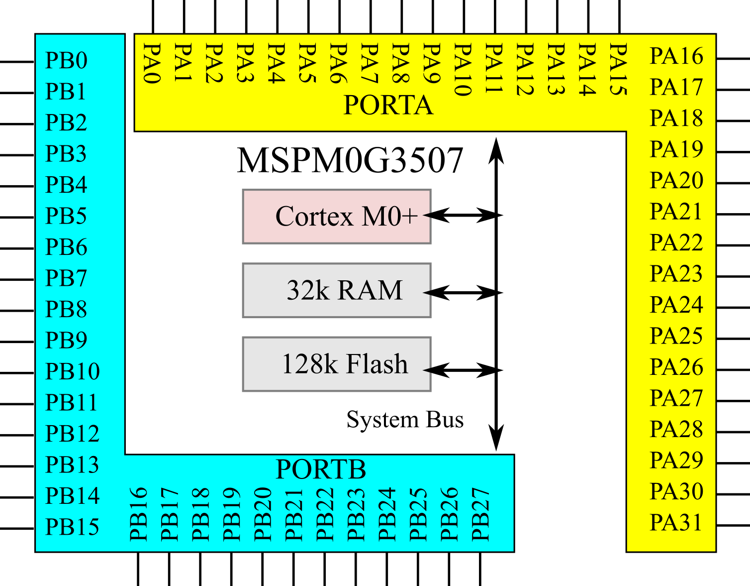
Figure 2.1.1. There are 60 I/O pins on the MSPM0G3507, grouped into two ports.
An interface is defined as the collection of the I/O port, external electronics, physical devices, and software, which combine to allow the computer to communicate with the external world. An example of an input interface is a switch, where the operator pushes or releases the switch, and the software can recognize the switch position. An example of an output interface is a light-emitting diode (LED), where the software can turn the light on and off, and the operator can see whether or not the light is shining. There is a wide range of possible inputs and outputs, which can exist in either digital or analog form. In general, we can classify I/O interfaces into four categories
Parallel - binary data are available simultaneously on a group of pins
Serial - binary data are available one bit at a time on a single pin
Analog - data are encoded as an electrical voltage, current, or power on a single pin
Time - data are encoded as a period, frequency, pulse width, or phase shift on a single pin
Video 2.1.1. Four categories of Input/Output Interfaces
The General Purpose Input Output (GPIO) port is a collection of input/output pins, and it allows the software to read data from input pins (Figure 2.1.2) and write data to output pins (Figure 2.1.3). Initialization software specifies whether a pin will be an input or output.
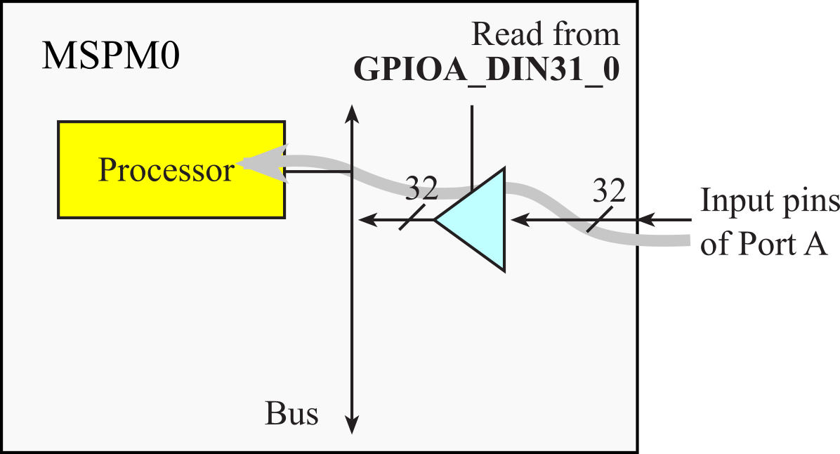
Figure 2.1.2. A GPIO input pins allows for input.
Video 2.1.2. A GPIO input pins allows for input.
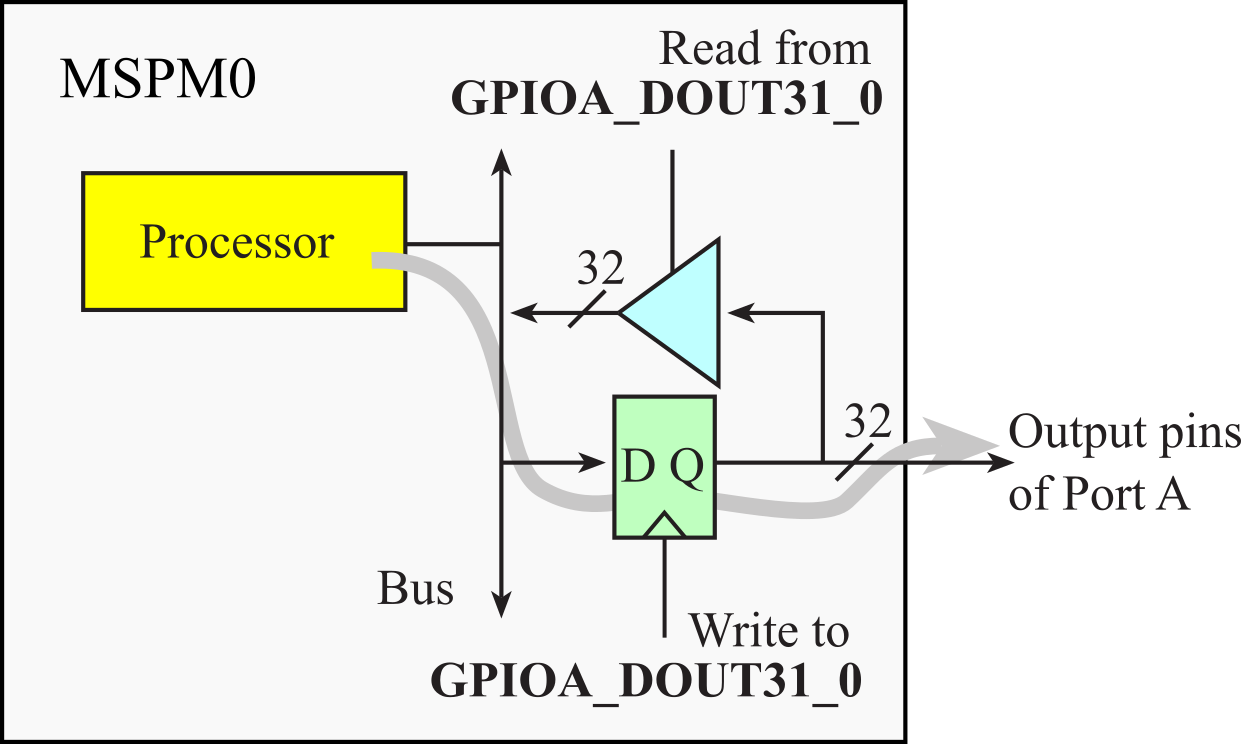
Figure 2.1.3. A GPIO output pins allows for output.
Video 2.1.3. Software writes to DOUT register to perform output.
An I/O register is a location in memory with which software can interface with the I/O port, see Table 2.1.1. On most embedded microcontrollers, the I/O ports are memory mapped. This means the software can access an input/output port simply by reading from or writing to the appropriate address. It is important to realize that even though I/O operations "look" like reads and writes to memory variables, the I/O ports often DO NOT act like memory. For example, some bits are read-only, some are write-only, some can only be cleared, others can only be set, and some bits cannot be modified. There are include statements for both assembly and C that will define symbolic names for the I/O registers as their corresponding addresses. To make our software easier to understand we will use the symbolic definitions for the I/O ports, like GPIOA_DOUT31_0, and not the specific address, like 0x400A1280.
| Address | Access | 31 | ... | 28 | 27 | ... | 1 | 0 | Name |
| 0x400A1280 | R/W | DIO31 | ... | DIO28 | DIO27 | ... | DIO1 | DIO0 | GPIOA_DOUT31_0 |
| 0x400A1380 | R | DIO31 | ... | DIO28 | DIO27 | ... | DIO1 | DIO0 | GPIOA_DIN31_0 |
| 0x400A3280 | R/W | - | - | - | DIO27 | ... | DIO1 | DIO0 | GPIOB_DOUT31_0 |
| 0x400A3380 | R | - | - | - | DIO27 | ... | DIO1 | DIO0 | GPIOB_DIN31_0 |
Table 2.1.1. I/O registers to perform input/output to Ports A and B.
There are many more registers with which we could perform I/O, but we will begin with these simple interactions:
- Read from GPIOA_DIN31_0 gets the current values of the input pins of Port A
- Write to GPIOA_DOUT31_0 sets the output pins of Port A
- Read from GPIOA_DOUT31_0 gets the last value written to GPIOA->DOUT31_0
- Read from GPIOB_DIN31_0 gets the current values of the input pins of Port B
- Write to GPIOB_DOUT31_0 sets the output pins of Port B
- Read from GPIOB_DOUT31_0 gets the last value written to GPIOB->DOUT31_0
The DIN31_0 register is read only. Writing to DIN31_0 has no effect. The DOUT31_0 register is read/write. The register DOUT31_0 does behave like regular memory.
The DOUTSET31_0 DOUTCLR31_0 DOUTTGL31_0 registers are write only, see Table 2.1.2. Reading from these registers has no effect. Writing 0's to these registers have no effect. Writing 1's to bits in these registers will modify the corresponding output pins. We use these three registers when different unrelated software modules need to access the same GPIO port.
| Address | Access | 31 | ... | 28 | 27 | ... | 1 | 0 | Name |
| 0x400A1290 | W | DIO31 | ... | DIO28 | DIO27 | ... | DIO1 | DIO0 | GPIOA_DOUTSET31_0 |
| 0x400A12A0 | W | DIO31 | ... | DIO28 | DIO27 | ... | DIO1 | DIO0 | GPIOA_DOUTCLR31_0 |
| 0x400A12B0 | W | DIO31 | ... | DIO28 | DIO27 | ... | DIO1 | DIO0 | GPIOA_DOUTTGL31_0 |
| 0x400A3290 | W | - | - | - | DIO27 | ... | DIO1 | DIO0 | GPIOB_DOUTSET31_0 |
| 0x400A32A0 | W | - | - | - | DIO27 | ... | DIO1 | DIO0 | GPIOB_DOUTCLR31_0 |
| 0x400A32B0 | W | - | - | - | DIO27 | ... | DIO1 | DIO0 | GPIOB_DOUTTGL31_0 |
Table 2.1.2. I/O registers to perform friendly output.
- Write 1s to DOUTSET31_0 to make the output pins go high
- Write 1s to DOUTCLR31_0 to make the output pins go low
- Write 1s to DOUTTGL31_0 to toggle the output pins (invert from 0 to 1 or 1 to 0)
The DOE31_0 register is configured once during initialization, see Table 2.1.3.
| Address | Access | 31 | ... | 28 | 27 | ... | 1 | 0 | Name |
| 0x400A12C0 | R/W | DIO31 | ... | DIO28 | DIO27 | ... | DIO1 | DIO0 | GPIOA_DOE31_0 |
| 0x400A32C0 | R/W | - | - | - | DIO27 | ... | DIO1 | DIO0 | GPIOB_DOE31_0 |
Table 2.1.3. We set bits in the Data output enable register make that GPIO pin an output.
Each of the 60 I/O pins on the MSPM0G3507 has a 32-bit Pin Control Management Register (PINCM). We write to this register once during initialization to configure the mode. Table 2.1.4 shows some of the bits we will configure.
| Name | Pin | ... | 18 | 17 | 18 | ... | 7 | 6 | 5-0 |
| IOMUXPA0 | PA0 | ... | INENA | PIPU | PIPD | ... | PC | - | PF |
| IOMUXPA1 | PA1 | ... | INENA | PIPU | PIPD | ... | PC | - | PF |
| ... | |||||||||
| IOMUXPB26 | PB26 | ... | INENA | PIPU | PIPD | ... | PC | - | PF |
| IOMUXPB27 | PB27 | ... | INENA | PIPU | PIPD | ... | PC | - | PF |
Table 2.1.4. Each port pin has a separate Pin Control Management Register, also called IOMUX.
- We set bit 18 INENA to specify the pin as input
- We set bit 17 PIPU to enable a pullup resistor on the input
- We set bit 16 PIPD to enable a pulldown resistor on the input
- We set bit 7 PC to allow software to input/output with the pin
- We set bits 5:0 PF to 00001 to specify GPIO mode.
: What do you suppose it means that PF is a 6-bit field?
Before we discuss hardware, let's develop a set of software functions that configure and use PB1 as an output and PB0 as an input. Program 2.1.1 shows software to initialize PB1 as an output. 0x81 is the magic code we write to the PINCM register to make the pin an output.
|
.include "../inc/msp.s" PB1_Init: // PB1 output MOVS R1,#0x81 LDR R0,=IOMUXPB1 // PINCM STR R1,[R0] // PB1 is GPIO LDR R0,=GPIOB_DOE31_0 LDR R1,[R0] // previous MOVS R2,#0x02 // mask ORRS R1,R1,R2 // friendly STR R1,[R0] // enable out BX LR |
#include "msp.h" void PB1_Init(void){ IOMUX->SECCFG.PINCM[PB1INDEX] = 0x81; GPIOB->DOE31_0 |= 0x02; // PB1 output; } |
Program 2.1.1. Software that initializes PB1 as an output.
: Change the assembly code to initialize PB2 as output.
Video 2.1.4. Initialization PB1 as output.
Program 2.1.2 shows software to initialize PB0 as an input. Writing the value 0x00040081 to the PINCM register specifies the pin as GPIO input without internal pull up or pull down resistors.
|
PB0_Init: // PB0 input LDR R1,=IOMUXPB0 // PINCM LDR R0,=0x00040081 STR R0,[R1] // GPIO input
BX LR |
void PB0_Init(void){ IOMUX->SECCFG.PINCM[PB0INDEX] = 0x00040081; } |
Program 2.1.2. Software that initializes PB0 as an input.
: Change the assembly code to initialize PB3 as input.
Video 2.1.5. Initialization PB0 as input.
Program 2.1.3 shows two functions that output to PB1. To change one bit in the port we read the previous values, modify the bit of interest, and then write the entire value back to the output register.
|
PB1_Set: // Make PB1 high LDR R0,=GPIOB_DOUT31_0 LDR R1,[R0] // previous MOVS R2,#0x02 // mask ORRS R1,R1,R2 // set bit STR R1,[R0] // output BX LR PB1_Clr: // Make PB1 low
LDR R0,=GPIOB_DOUT31_0 LDR R1,[R0] // previous MOVS R2,#0x02 // mask BICS R1,R1,R2 // clear bit STR R1,[R0] // output BX LR |
void PB1_Set(void){ // Make PB1 high
GPIOB->DOUT31_0 |= 0x02; // PB1=1; } void PB1_Clr(void){ // Make PB1 low
GPIOB->DOUT31_0 &= ~0x02; // PB1=0; } |
Program 2.1.3. Software outputs to PB1.
: Change the assembly code so it outputs to PB2 instead of PB1.
Video 2.1.6. Software that outputs to PB1.
Program 2.1.4 presents a function that inputs from PB0. To read one bit in the port, we read the entire DIN31_0 register, and then we select the bit of interest using the logical AND operation.
|
// Return R0 with value of PB0 PB0_In: // read PB0 LDR R1,=GPIOB_DIN31_0 LDR R0,[R1] // all bits MOVS R2,#0x01 // mask ANDS R0,R0,R2 // select bit BX LR |
uint32_t PB0_In(void){ // Read PB0
return GPIOB->DIN31_0&0x01; } |
Program 2.1.4. Software inputs from to PB0.
: Change the assembly code so it inputs from PB3 instead of PB0.
Video 2.1.7. Software that inputs from PB0.
Quiz 2.1
2.2. MSPM0G3507 LaunchPad
The heart of the LaunchPad is the MSPM0G3507 microcontroller. The LaunchPad evaluation board (Figure 2.2.1) is a low-cost development board available as part number LP-MSPM0G3507. The microcontroller board provides an integrated In-Circuit Debug Interface (ICDI), which allows programming and debugging of the onboard MSPM0G3507 microcontroller. The USB cable is used by the debugger (ICDI), and it includes a serial port (UART) to send data to the PC.
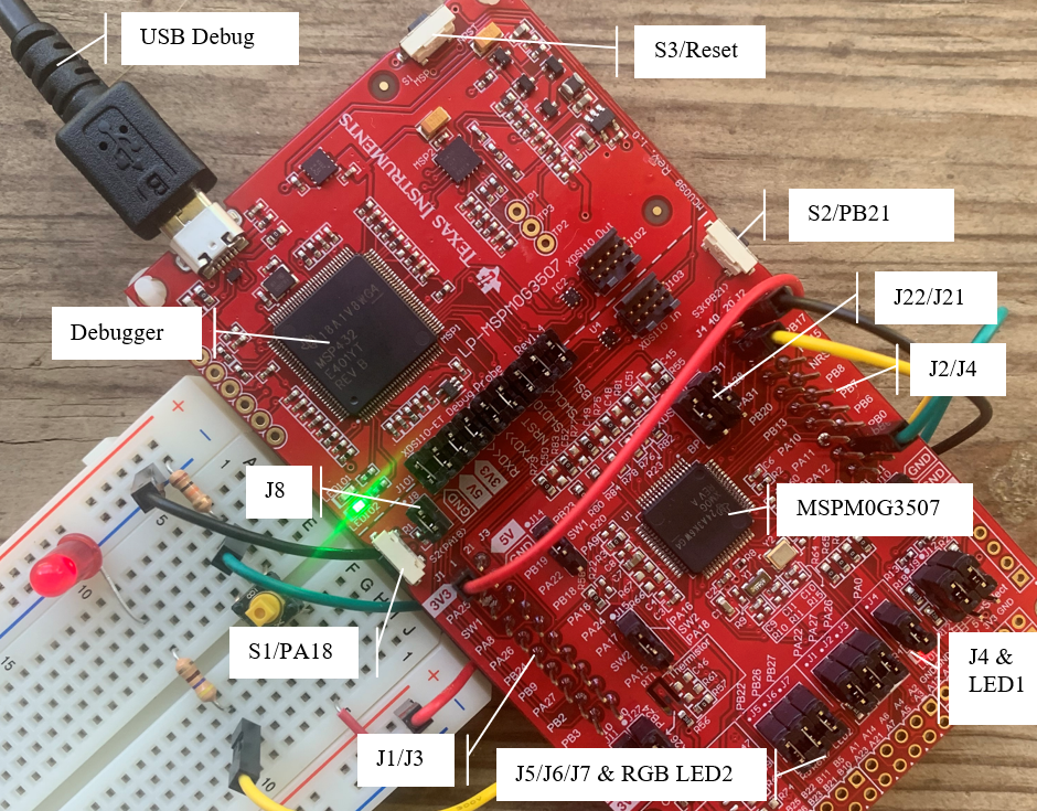
Figure 2.2.1. LaunchPad based on the MSPM0G3507.
Video 2.2.1. Overview of MSPM0G3507 LaunchPad
Sometimes we run bad code on the MSPM0, and the code crashes hard. Other times we try a weird sequence of debugging commands and the debugger freezes. In both cases, we might put the MSPM0 in a state where it can not be programmed. We call this failure state bricked. A bricked MSPM0 shows red error messages when trying to program a project that used to work. We can unbrick the MSPM0 by forcing a physical reset of the bootstrap loader. The BSL_Invoke button is labelled S1 and is located near LED1. The reset button is on the same edge as the USB cable. To unbrick the MSPM0, we
- Press-and-hold S1
- Press and release the Reset button (while holding S1)
- Within the next 10secs, attempt to program the MSPM0, Debug command
- After download is complete, release S1.
Video 2.2.2. How to unbrick the MSPM0G3507.
If the board seems very dead, try performing a factory reset:
https://dev.ti.com/gallery/view/TIMSPGC/MSPM0_Factory_Reset_Tool/ver/1.0.2/
We will begin by interacting with the switches and LEDs on the LaunchPad. For example, bit 0 of Port A is called PA0 and it controls the red LED on the LaunchPad. Figure 2.2.2 shows there are switches connected to PA18 and PB21. There is one 3-color LED connected to PB22-PB27-PB26. The MSPM0 LaunchPad evaluation board has two switches, one red LED1 and one 3-color LED2. See Figure 2.2.2. The S1 switch is positive logic. The S2 switch is negative logic and will require activation of the internal pull-up resistor. See the LaunchPad.c file for software to configure the LaunchPad I/O. Pins PA11-PA10 create a serial port, which is linked through the debugger cable to the PC. The serial link is a physical UART as seen by the MSPM0 and mapped to a virtual COM port on the PC.
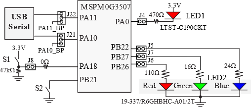
Figure 2.2.2. Switch and LED interfaces on the MSPM0G3507 LaunchPad Evaluation Board. The jumpers J4 J5 J6 J7 J8 can be removed so the corresponding pin can be used for its regular purpose.
Video 2.2.3. MSPM0 LaunchPad Circuit***needs recording***
: How does the software input from Port A?
: How does the software output to Port B?
The following tool allows
you to test your understanding of what happens when you WRITE to the DOUT
register for Port A or Port B.
Note, writing to input pins has no effect. See what happens if you click
on one of the two switches.
In most cases, a software module needs access to only some of the port pins. If two or more software modules access the same port, a conflict will occur if one module changes modes or output values set by another module. It is good software design to write friendly software, which only affects the individual pins as needed. Friendly software does not change the other bits in a shared register. Conversely, unfriendly software modifies more bits of a register than it needs to. The difficulty of unfriendly code is each module will run properly when tested by itself, but weird bugs result when two or more modules are combined.
Video 2.2.4. Writing friendly code
The best way for microcontrollers to access individual port bits is to use read-modify-write software to change just the bits of interest. A read-or-write sequence can be used to set bits. Recall from Figure 2.2.2 there is a three color LED connected to PB27,PB26,PB22. Program 2.2.1 presents software that writes 1's to PB27,PB26,PB22 in a friendly manner, making the LED white.
|
TurnOnLED: LDR R1, =GPIOB_DOUT31_0 LDR R0, [R1] // previous // R2 is the mask for bits 27,26,22 LDR R2,=((1<<27)|(1<<26)|(1<<22)) ORRS R0, R0, R2 // set bits 27,26,22 STR R0, [R1] // perform output BX LR |
// make PB27,PB26,PB22 high void TurnOnLED(void){ GPIOB->DOUT31_0 |= ((1<<27)|(1<<26)|(1<<22)); } |
Program 2.2.1. Software to turn on the 3-color LED.
: What does (1<<27) mean?
A read-and-write sequence can also be used to clear one or more bits. Program 2.2.2 presents software that writes 0's to PB27,PB26,PB22 in a friendly manner, turning the LED off.
|
TurnOffLED: LDR R1, =GPIOB_DOUT31_0 LDR R0, [R1] // previous // R2 is the mask for bits 27,26,22 LDR R2,=((1<<27)|(1<<26)|(1<<22)) BICS R0, R0, R2 // clear bits STR R0, [R1] // perform output BX LR |
// make PB27,PB26,PB22 low void TurnOffLED(void){ GPIOB->DOUT31_0 &= ~((1<<27)|(1<<26)|(1<<22)); } |
Program 2.2.2. Software to turn off the 3-color LED.
The red LED on the LaunchPad is negative logic, so in Program 2.2.3 we clear PA0 to turn on the LED, and in Program 2.2.4 we set PA0 to turn the LED off. In both cases, code is friendly because the software does not affect the other 31 bits of GPIOA_DOUT31_0.
|
LaunchPad_LED1on: LDR R1, =GPIOA_DOUT31_0 LDR R0, [R1] // previous MOVS R2,#0x01 BICS R0, R0, R2 // clear bit 0 STR R0, [R1] // perform output BX LR |
// make PA0 low void LaunchPad_LED1on(void){ GPIOA->DOUT31_0 &= ~0x01; } |
Program 2.2.3. Software to turn on the red LED.
|
LaunchPad_LED1off: LDR R1, =GPIOA_DOUT31_0 LDR R0, [R1] // previous MOVS R2,#0x01 // mask ORRS R0, R0, R2 // set bit 0 STR R0, [R1] // perform output BX LR |
// make PA0 low void LaunchPad_LED1off(void){ GPIOA->DOUT31_0 |= 0x01; } |
Program 2.2.4. Software to turn off the red LED.
Maintenance Tip: When performing output to pins, remember to store a new value to the port. Actual output comes when we write to the DOUT register.
Quiz 2.2
2.3. Interfacing the Microcontroller to a solderless breadboard
To build circuits, we’ll use a solderless breadboard, also referred to as a protoboard. The holes in the protoboard are internally connected in a systematic manner, as shown in Figure 2.3.1. The long rows of holes along the outer sides of the protoboard are electrically connected. Some protoboards like the one in Figure 2.3.1 have four long rows (two on each side), while others have just two long rows (one on each side). We refer to the long rows as power buses. If your protoboard has long rows on the side, we will connect one long row to +3.3V and another long row to ground. In the middle of the protoboard, you’ll find two groups of holes placed in a 0.1 inch grid. Each adjacent row of five pins is electrically connected. We insert components like resistors, switches and LEDs into these holes. If integrated circuits (IC) are to be placed on the protoboard, it is done such that the two rows of pins straddle the center valley.
Video 2.3.1. Connecting PB0 and PB1 to a solderless breadboard.
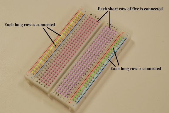
Figure 2.3.1. The pins on each of the four long rows are connected. The 5 pins in each short row are connected. Place a +3.3V wire from the Launchpad to one long row. Place a ground wire from the LaunchPad to another long row.
To build a circuit and to connect the circuit to the microcontroller we will use 22-gauge or 24-gauge solid wires. We strip off about 1/4 to 1/2 inch of insulation so the bare wire can be pushed straight into a hole. We only push one wire into a hole keeping track of which rows are internally connected.
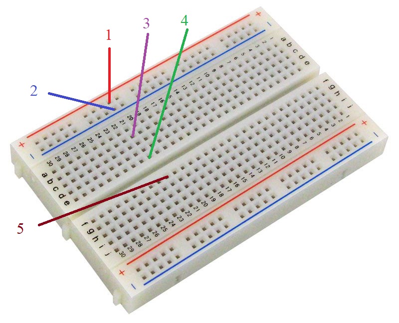
Figure 2.3.2. Solderless breadboard used in the following checkpoints.
: In Figure 2.3.2, the five colored lines represent wires plugged into the protoboard. All five wires are plugged into row 21. Which wires are connected via the protoboard?
: In Figure 2.3.2, what is the typical use of the long row of connections near the red line?
: In Figure 2.3.2, what is the typical use of the long row of connections near the blue line?
Quiz 2.3
2.4. Software Delay Loops
Time is one of the most important aspects of an embedded system. Throughout the course we will develop more complex, but more accurate methods for the software to control when events occur. We will begin with the most simple, a software delay loop. When performing Labs 2 and 3 with software delay loops, you will witness this method is inaccurate and hard to manage. Therefore for Labs 2 and 3 we expect the timing to be approximate. Lab 4 will introduce a hardware timer, and Lab 5 will introduce interrupts. Program 2.4.1 shows one possible way to create a software delay loop. First, we note that our Micrrocontroller's default Clock runs at 32MHz. However, the use of a Phase Lock Loop (PLL) allows us to run the Microcontroller at different speeds, from a minimum of 4MHz up to a maximum of 80MHz. In this text we assume we are runnning at 80MHz. This means, there are 80 x 106 bus cycles in one second, or each bus cycle takes 1/(80 x 106) = 12.5ns (nanoseconds). Instructions on the microcontroller take some number of bus cycles depending upon how much work is involved. For example, most Arithmetic, Logic and Shift operations take 1 bus cycle. LDR and STR take 2 bus cycles. The B ranch instruction takes 1 bus cycle if the branch is not taken and 2 bus cycles if the branch is taken, as taking the branch involves modifiication of the PC. You can find more details about cycle count of instructions in section 3.3. of the Arm Cortex-M0+ Technical Reference Manual.
The Delay subroutine implemented below runs for count cycles, where count is passed in R0. We have a loop (dloop) with 3 instructions in it that take a total of 4 bus cycles: SUBS takes 1, BHS takes 2 and we added the NOP so the total is 4. With a R0 value of count, the loop would take (4 x count) cycles to run. If we wnt it to run for count cycles, we simply make SUBS count in steps of 4, hence the decrement by 4. To get a precise delay, we have to account for the fact that the instruction BX LR itself takes 1 bus cycle, so we start with a count of 1 less than the desired count, which is the purpose of the first SUBS (outside the dloop). This SUBS itself takes 1 bus cycle, so we have to start the dloop with a count 2 less than the desirred value. Now, with a bus clock of 80 MHz, this delay function delays for precisely 12.5ns*count, where count is the integer passed in register R0. In Program 2.4.2 we call Delay with R0 equal to 40 million, which will wait for 40*106 *12.5*10-9 = 500 ms (or half a second). To determine the actual delay you will have to run this code on your microcontroller and measure the delay with a scope or logic analyzer.
//
Input: R0 is count, the amount to delay in bus cycles
.align 2
Delay: SUBS R0,R0,#2
dloop: SUBS R0,R0,#4 // 4 cycles per loop
NOP
BHS dloop
BX LR
Program 2.4.1. Software delay loop.
: In the Program 2.4.1, why do we subtract 2 once?
: In the Program 2.4.1, why do we subtract 4 each time through the loop?
Video 2.4.1. Using a software delay loop to toggle an LED.
|
main: MOVS R0,#0 |
int main(void){ |
Program 2.4.2. LED toggles every 500ms. See Programs 2.2.3 and 2.2.4.
: Write assembly code to delay 1 second.
2.5. Switch/button Interfacing
Before interfacing switches, let's explain how an input port converts voltage into digital logic. Most pins on the MSPM0 microcontrollers are not 5V-tolerant, meaning an input voltage above 3.6 V will be damage the chip. Similiarly, input voltages below 0 will also damage the chip. Voltages from 2.31 to 3.3 V are considered high, and voltages from 0 to 0.99 V will be considered as low. Since the microcontroller is built with CMOS logic, the input current will be less than 50 nA. This is so small, for most situtations, we can assume the input current is 0.
- VIH = 2.31V is the voltage above which the input is considered high.
- VIL = 0.99V is the input voltage below which the input is considered low.
- IIH ≤ 50nA is the current into the pin when the input is high.
- IIL ≤ 50nA is the current into the pin when the input is low.
The first input device we will interface is the switch. Once manipulated by a human, a toggle switch remains in its on or off position. In contrast, a tactile switch or button remains in the on position only when pressed by the human. The button returns to the off position when released by the human.
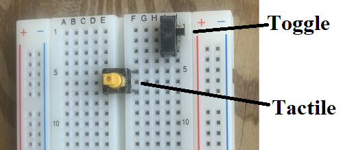
Figure 2.5.1. Two kinds of switches: toggle and tactile.
Switches allow the human to input binary information into the computer. Typically we define the asserted state, or logic true, when the switch is pressed. Contact switches can also be used in machines to detect mechanical contact (e.g., two parts touching, paper present in the printer, window open/closed, or wheels on the ground etc.) A single pole single throw (SPST) switch has two connections as shown in Figure 2.5.2. In a normally open switch (NO), the resistance between the connections is infinite (over 100 MΩ on the B3F tactile switch) if the switch is not pressed, and the resistance is zero (under 0.1 Ω on the B3F tactile switch) if the switch is pressed.
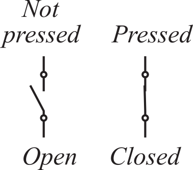
Figure 2.5.2. Single Pole Single Throw (SPST) Switch interface. When not pressed, the switch is open (over 100MΩ). When pressed, the switch is closed (under 0.1Ω).
We encourage you to read the data sheet for your switch and find which pins connect to the switch. Data sheet for the B3F-1059
Video 2.5.1. B3F Switch Datasheet
To convert the 100MΩ/0.1Ω resistance into a digital signal, we can use a pull-down resistor to ground or a pull-up resistor to +3.3V as shown in Figure 2.5.3. Notice that 10 kΩ is 100,000 times larger than the on-resistance of the switch and 10,000 times smaller than its off-resistance. Another way to choose the pull-down or pull-up resistor is to consider the input current of the microcontroller input pin. The current into the microcontroller will be less than 50 nA (shown as IIL and IIH in the data sheet). So, if the current into microcontroller is 50 nA, then the voltage drop across the 10 kΩ resistor will be 0.0005 V, which is negligibly small. With a pull-down resistor shown on the right side of Figure 2.5.3, the digital signal will be low if the switch is not pressed and high if the switch is pressed. The signal being 3.3V when the switch is pressed is defined as positive logic, because the asserted switch state is a logic high. Conversely, with a pull-up resistor shown on the left side of Figure 2.5.3, the digital signal will be high if the switch is not pressed and low if the switch is pressed. The signal being 0V when the switch is pressed is defined as negative logic, because the asserted switch state is a logic low.

Figure 2.5.3. Two ways to interface a Single Pole Single Throw (SPST) Switch to the microcontroller.
: On the left side of Figure 2.5.2, when the switch is pressed, will the signal s be a logic 0 or logic 1?
: On the right side of Figure 2.5.2, when the switch is pressed, will the signal t be a logic 0 or logic 1?
Video 2.5.2. Circuit for Switch Interface (note: input current is 50nA, not 2uA)
To interface a switch we connect it to a pin, and we initialize the pin as an input. Figure 2.5.4 connects the switch to PA8, but any microcontroller pin could have been used.
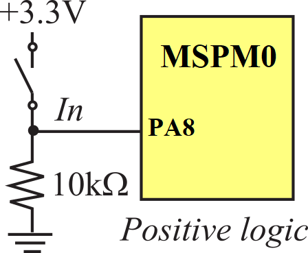
Figure 2.5.4. Interface of a switch to a microcomputer input.
Figure 2.5.5 shows how we could build this circuit with a protoboard and a LaunchPad. The brown-black-orange resistor is 10kΩ. The B3F switch should plug directly into the protoboard. The actual switch is across the pins that are closer to each other. The pins that are farther from each other will fit across the gap in the middle of the protoboard. It doesn't matter what color the wires are, but in this figure the wires are black, purple and blue. The two black wires are ground, the two purple wires are +3.3V, and the blue wire is the signal in, which connects the switch to pin PA8 of the microcontroller.
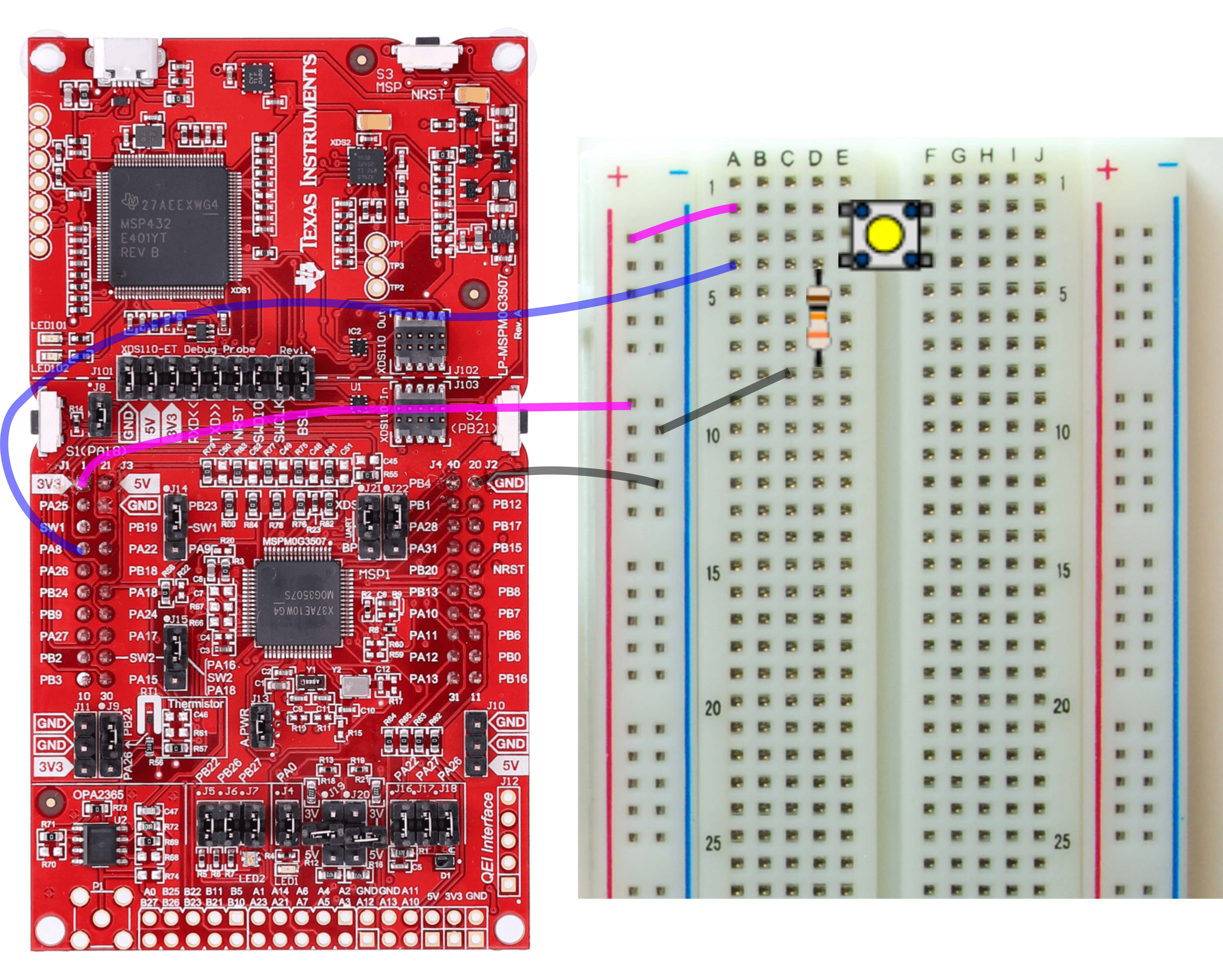
Figure 2.5.5.
Construction of the interface of a B3F switch to a microcomputer input on PA8.
: Notice the switch in Figure 2.5.4 has four connections to the breadboard, but the switch in Figure 2.5.4 circuit only has two connections. What are the two extra connections on the actual switch?
The initialization function will set the direction register to input and enable the pin. This code assumes LaunchPad_Init() has been called. The function LaunchPad_Init() should be called exactly once at the start of the system, because it will reset all of Port A and Port B. Notice the software is friendly because it just affects PA8 without affecting the other bits in Port A. The input function reads Port A and returns a true (0x100) if the switch is pressed and returns a false (0) if the switch is not pressed. The software in Program 2.5.1 is called a driver, and it includes an initialization, which is called once, and a second function that can be called to read the current state of the switch. Writing software this way is called an abstraction, because it separates what the switch does (Init and Input) from how it works (PortA, bit 5, and MSPM0). The input function reads the entire port and selects bit 5 using a logical AND.
|
// Assembly version |
// C version |
Program 2.5.1. Software interface for a switch on PA8.
Maintenance Tip: When interacting with just some of the bits of an I/O register it is better to modify just the bits of interest, leaving the other bits unchanged. In this way, the action of one piece of software does not undo the action of another piece. Modifying just the bits of interest is called friendly.
Observation: One of the complicating issues with mechanical switches is they can bounce (oscillate on and off) when touched and when released. The contact bounce varies from switch to switch and from time to time, but usually bouncing is a transient event lasting less than 5 ms. We can eliminate the effect of bounce if we design software that waits at least 10 ms between times we read the switch values.
: What does it mean to classify this switch interface as positive logic?
Quiz 2.5
2.6. LED Interfacing
Before interfacing LEDs, let's review how an output port converts digital logic into voltage. Pins PA31, PA28, PA11, and PA10 can be high drive outputs, sourcing/sinking up to 20mA. The remaining pins are standard drive and can source or sink up to 6mA as an output.
- VOH ≥ 2.9V is the voltage when the output is high.
- VOL ≤ 0.4V is the voltage when the output is low.
- IOH ≤ 6 mA is the current out of the pin when the output is high.
- IOL ≤ 6 mA is the current out of the pin when the output is low.
A light emitting diode (LED) emits light when an electric current passes through it. LEDs have polarity, meaning current must pass from anode to cathode to activate, see Figure 2.6.1. The anode is labelled a or + , and cathode is labelled k or -. The cathode is the short lead and there may be a slight flat spot on the body of round LEDs. Thus, the anode is the longer lead. The brightness of an LED depends on the applied electrical power (P=Vd*Id). Notice in the LED operating range of 5 to 40 mA, the voltage only changes from 1.8 to 2.2V. For this reason, we will establish the desired brightness by setting the LED current rather than trying to set the LED voltage.
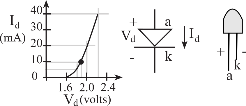
Figure 2.6.1. Positive logic LED interface (Lite-On LTL-4213).
: Notice black dot in Figure 2.9 shows Vd=1.9V and Id=10mA for a power of 19mW. What would be the LED power if the LED voltage were to increase just a little bit toVd=2V?
We encourage you to open up the data sheet for your LED and find the curve similar to Figure 2.6.1. See the data sheet for HLMP-4700 or LTL-4213.
Video 2.6.2. Circuit for LED Interface
When the LED current is less than 6 mA, we can interface it directly to an output pin without using any integrated circuits. The HLMP-4700 LED shown in Figure 2.6.2a has an operating point of 1.6 V and 1 mA.

Figure 2.6.2. Interface of a low current LED, like the HLMP-4700.
For the positive logic interface (Figure 2.6.2b) we calculate the resistor value based on the desired LED voltage and current
R = (VOH
- Vd) / Id =
(3.1 -
1.6) /0.001 =
1500Ω
where VOH is the output high voltage of the microcontroller output pin, which will be about 3.1V when sourcing 1mA of current. Since VOH can vary from 2.4 to 3.3 V, it makes sense to choose a resistor from a measured value of VOH, rather than the minimum value of 2.4 V. Negative logic means the LED is activated when the software outputs a zero. For the negative logic interface (Figure 2.6.2c) we use a similar equation to determine the resistor value
R = (3.3 - Vd
-
VOL ) / Id =
(3.3 - 1.6 - 0.2) /0.001 =
1500Ω
where VOL
is the output low voltage of the microcontroller output pin, which will be about
0.2V when sinking 1mA of current. Since VOL can
vary from 0 to 0.4 V, it makes sense to choose a resistor from a
measured value of VOL, rather than the maximum
value of 0.4 V.
Figure 2.6.3 shows how we could build this circuit with a protoboard and a LaunchPad. The brown-green-red resistor is 1.5kΩ. The LED should plug directly into the protoboard. The longer lead on the LED is the positive or anode. It doesn't matter what color the wires are, but in this figure the wires are black, red and green. The two black wires are ground, and the green wire is the signal out, which connects the LED anode to pin PB1 of the microcontroller.
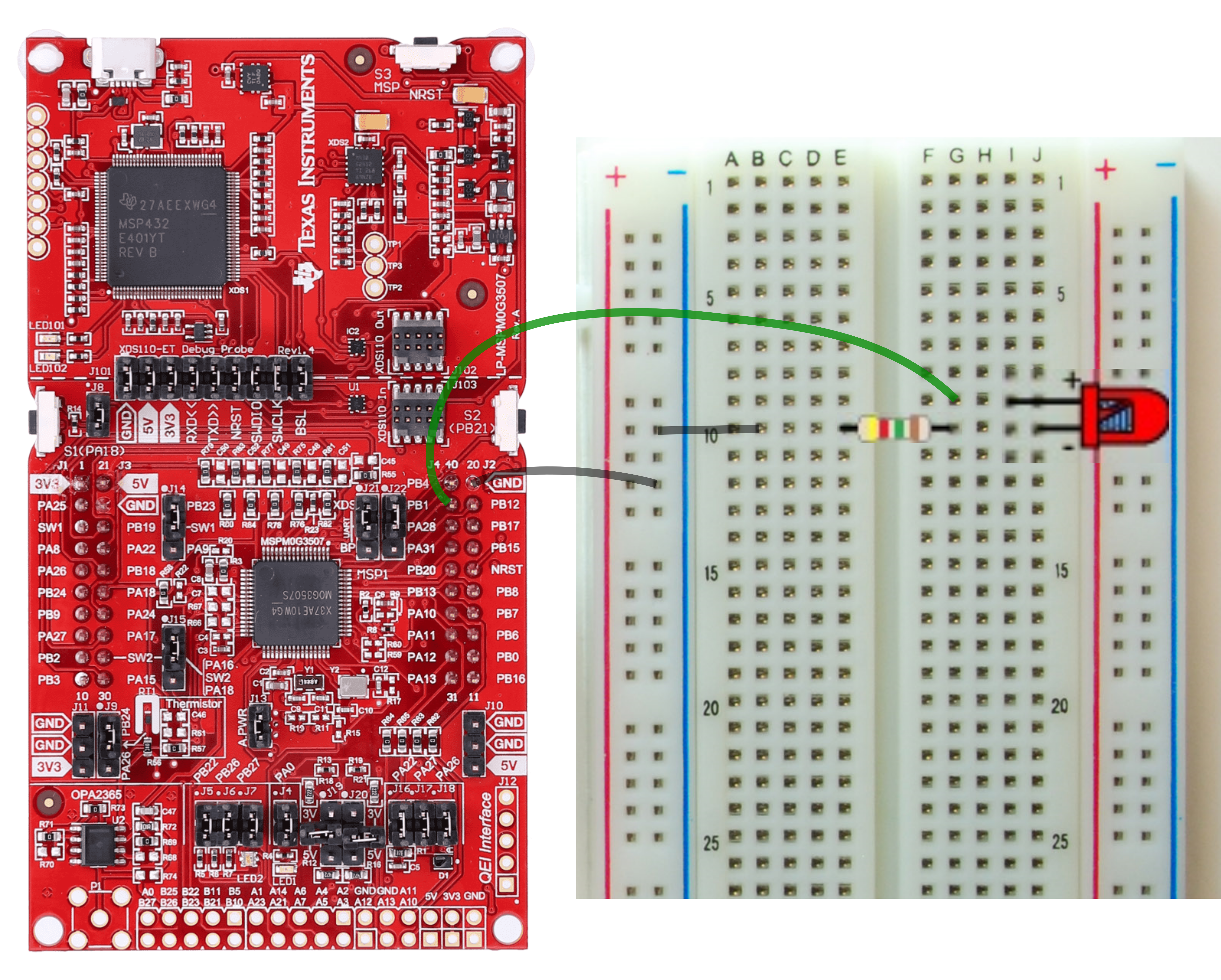
Figure 2.6.3.
Construction of the interface of an LED to the PB1 output.
: What resistor value in of Figure 2.6.2 is needed if the desired LED operating point is 1.8V and 5 mA? Use the positive logic interface and, VOH of 3.2V.
: What resistor value in of Figure 2.6.2 is needed if the desired LED operating point is 1.7V and 2 mA? Use the negative logic interface and, VOL of 0.2V.
A driver or firmware is a set of software functions to facilitate the use of an input/output port. Program 2.6.1 is an simple example of driver because it encapulates everything we might wish to do with an LED. Drivers will include an initialization, e.g., LED_Init, which is called once at the beginning. The other functions in the driver can be called to turn on and off the LED as needed. Writing software this way is called an abstraction, because it separates what the LED does (Init, On, Off) from how it works (PortB, bit 1, MSPM0). Program 2.6.1 shows two ways to change PB1. Both ways are friendly, but using the DOUTSET and DOUTCLR registers is faster and simpler. This code assumes LaunchPad_Init has been called.
|
// Assembly version |
// C version |
Program 2.6.1. Software driver for an LED on PB1
: What does it mean to classify this LED interface as positive logic?
Observation: One of the advantages of using DOUTSET and DOUTCLR is the software becomes thread-safe, meaning it will operate properly when executed in a system with interrupts. Programs LED_OnSlow and LED_OffSlow have critical sections, meaning they will not operate properly when executed in a system with interrupts. We will learn more about critical sections in Chapter 8.
If the LED current is above 6 mA, like the LTL-4213, we cannot connect it directly to the microcontroller because the high currents may damage the chip. There are many possible solutions to interface an LED needing more than 8 mA of current. Examples include 7405, 7406 or PN2222. We have chosen the ULN2003 because it has 7 drivers in each package. The ULN2003 comes in a DIP package with 7 base (B) signals, 7 collector (C) signals and one emitter (E) pin. Figure 2.6.4 shows one driver in the ULN2003.The B signals are the inputs, the C signals are the outputs, and the E pin will be grounded. If the base input is high, the collector output will be low (0.5V). If the base input is low, the collector output will float (neither high nor low).
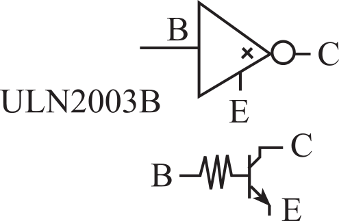
Figure 2.6.4. The ULN2003 LED driver with 7 darlington N-channel transistors.
For high current LEDs we typically use the 5V supply
rather than the 3.3V, because the available current at 5V is often much
more than the available current at 3.3V. Figure 2.6.5 shows how to
interface a 10 mA 1.9V LED using the ULN2003. When the software writes a
logic 1 to the output port, the input to the ULN2003 becomes high, output
from the ULN2003 becomes low, 10 mA travels through the LED, and the LED
is on. When the software writes a logic 0 to the output port, the input to
the ULN2003 becomes low, output from the ULN2003 floats (neither high
nor low), no current travels through the LED, and the LED is dark.
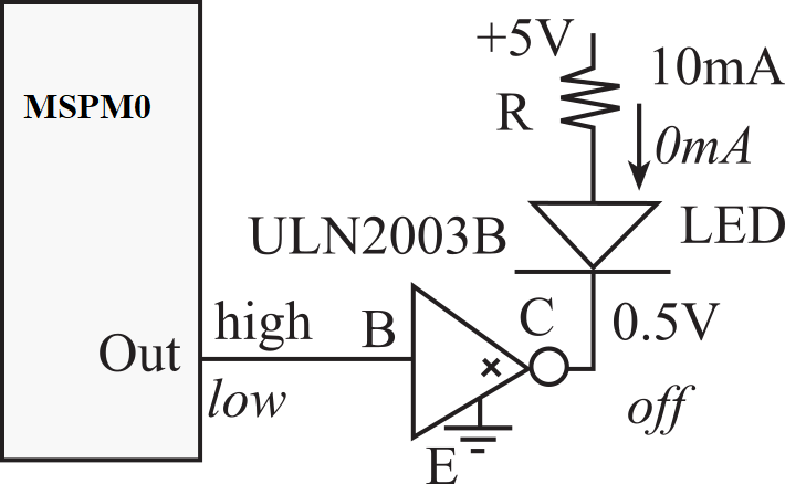
Figure 2.6.5. Interface a high current LED using a ULN2003 driver.
The value of the resistor is selected to establish the proper LED current. When active, the LED voltage will be between 1.8 and 2.2 V, and the power delivered to the LED will be controlled by its current. If the desired brightness requires an operating point of 1.9 V at 10 mA, then the resistor value should be
R = (5 - Vd - VCE) / Id = (5 - 1.9- 0.5) /0.01 = 260Ω
where Vd, Id is the desired LED operating point, and VCE is the output low voltage of the LED driver. If we use a standard resistor value of 270Ω in place of the 260Ω, then the current will be (5-1.9-0.5V)/270Ω, which is about 9.6 mA. This slightly lower current is usually acceptable.
: What resistor value in Figure 2.6.5 is needed if the desired LED operating point is Vd=1.7V and Id=11 mA?
: What resistor value in Figure 2.6.5 is needed if the desired LED operating point is Vd=2.1V and Id=25 mA?
Quiz 2.6
2.7. Pulse width modulation
Controlling time is an important function of an
embedded system. One of the methods software can perform to set the
delivered power to an external device is pulse width modulation
(PWM). The basic idea is to oscillate an output so fast the external
device does not respond to the individual on and off events. Rather, the
delivered power will be a function of the average, called duty cycle.
Let H be the time the output is high, and L the time the output is low.
For PWM we will set P=H+L as a constant, and adjust H and L. The duty
cycle is defined as
Duty Cycle = H/(H+L)
The human eye can see a flashing LED up to about 10
Hz. If we flash the LED at 100 Hz, our eyes will see a constant light, but
the brightness of the LED will depend linearly on the duty cycle. In
particular if the LED operating point is Vd, Id,
the LED power will be
Power = Vd*Id*H/(H+L)
Video 2.7.1. Pulse Width Modulation ***needs recording.
Program 2.7.1 presents a simple PWM output. Notice that
this implementation uses all the processor time. H can vary from 4 to 799996 bus cycles,
while L varies from 799996 to 4. H+L should be constant, in this example 800,000*12.5ns = 10ms.
|
main: MOVS R0,#0 |
int main(void){ |
Program 2.7.1. Software implementation of 75% PWM (see also Program 2.6.1).
: If H+L=100000, creating a 100 Hz wave in Program 2.7.1, how many different duty cycles can be created? How bits of precision does this represent?
The following tool allows you see the effect of Period and DutyCycle in Program 2.7.1. Dragging the slider bars sets H+L to Period, and set H to Period*DutyCycle.
: Drag the handle to set the period to be about 500ms. At what rate should the LED be flashing?
: What do your eyes observe if the period is less than 50ms?
: As you drag just the duty cycle bar left and right, does the period change?
Observation: Using PWM we can create virtually any color on the 3-color LED. For example, the burnt orange color code for the Texas Longhorns logo is Pantone: PMS 159 C, Hex Color: #BF5700, RGB: (191, 87, 0). To make burnt orange we oscillate the red signal at a duty cycle of 191/255, oscillate green at a duty cycle at 87/255, and set the blue signal to 0.
Quiz 2.7
2.8. Designing a Security System
Some problems are so unique that they require the engineer to invent completely original solutions. Most of the time, however, the engineer can solve even complex problems by building the system from components that already exist. Creativity will still be required in selecting the proper components, making small changes in their behavior (tweaking), arranging them in an effective and efficient manner, and then verifying the system satisfies both the requirements and constraints. When young engineers begin their first job, they are sometimes surprised to see that education does not stop with college graduation, but rather is a life-long activity. In fact, it is the educational goal of all engineers to continue to learn both processes (rules about how to solve problems) and products (hardware and software components). As the engineer becomes more experienced, he or she has a larger toolbox from which processes and components can be selected.
The hardest step for most new engineers is the first one: where to begin? We begin by analyzing the problem to create a set of specifications and constraints in the form of a requirements document. Next, we look for components, in the form of previously debugged solutions, which are similar to our needs. Often during the design process, additional questions or concerns arise. We at that point consult with our clients to clarify the problem. Next we rewrite the requirements document and get it reapproved by the clients.
It is often difficult to distinguish whether a parameter is a specification or a constraint. In actuality, when designing a system it often doesn’t matter into which category a parameter falls, because the system must satisfy all specifications and constraints. Nevertheless, when documenting the device it is better to categorize parameters properly. Specifications generally define in a quantitative manner the overall system objectives as given to us by our customers.
Constraints, on the other hand, generally define the boundary space within which we must search for a solution to the problem. If we must use a particular component, it is often considered a constraint. In this class, we constrain most designs to include a MSPM0 LaunchPad. Constraints also are often defined as an inequality, such as the cost must be less than $50, or the battery must last for at least one week. Specifications on the other hand are often defined as a quantitative number, and the system satisfies the requirement if the system operates within a specified tolerance of that parameter. Tolerance can be defined as a percentage error or as a range with minimum and maximum values.
In engineering everything is either a system or an interface between systems. For example a switch can be considered a system. When we interface it to the LaunchPad the switch-LaunchPad combination is a new system. Therefore, we begin by collecting the components required to build the system. We then combine the components and debug the system. As the components are combined we create new more powerful components. When writing software, we can use flowcharts to develop new algorithms. The more we can simulate the system, the more design possibilities we can evaluate, and the quicker we can make changes. Debugging involves both making sure it works, together with satisfying all requirements and constraints.
2.8.1. Requirements
First, lets develop a requirements document. The main purpose of a requirements document is to serve as an agreement between you and your clients describing what the system will do. This agreement can become a legally binding contract. Write the document so that it is easy to read and understand by others. It should be unambiguous, complete, verifiable, and modifiable.
The requirements document should not include how the system will be designed. This allows the engineer to make choices during the design to minimize cost and maximize performance. Rather it should describe the problem being solved and what the system actually does. It can include some constraints placed on the development process. Ideally, it is co-written by both the engineers and the non-technical clients. However, it is imperative that both the engineers and the clients understand and agree on the specifics in the document.
Video 2.8.1. Requirments Document
Requirements document for the security system
- Overview
- Objectives: Design a security system with two sensors and one alarm. Contact switches will be used for the sensors. If the window is secure the switch will be pressed, and if the window is open, the switch will be released. The alarm condition will be a flashing LED. The system can be activated/deactivated with a toggle switch.
- Process: We will first prototype it on a breadboard using a LaunchPad, two momentary switches, a toggle switch, and an LED. Hardware and software designs will be developed and tested. Once the prototype is tested, the momentary switches can be replaced with switches that fit into the windows and doors, and the flashing LED can be replaced with an audio alarm. The number of sensors will need to be increased to allow one sensor to be placed in each window and door of the house.
- Roles and Responsibilities: Dr. Yerraballi will develop the hardware and Dr. Valvano will develop the software, both will test.
- Interactions with Existing Systems: We will use a LaunchPad. It will be powered through the USB cable either with AC outlet or stand-alone battery. The components of the prototype will be selected, if possible, from the parts in the lab kit.
- Terminology: A momentary switch has a spring, such that if no force is applied the contact will be open. Applying force continuously will close the contact on the momentary switch. A toggle switch can be placed in either the open or closed state, and force is required to change from open to closed or from closed to open.
- Security: The wires between the sensors and the microcontroller will need to be hidden. However, cutting the wires should constitute a breach, setting off the alarm.
- Function Description
- Functionality: There are two contact switches that measure the status of your home. Each contact switch is positioned in the frame of a window or a door. If the switch is closed or pressed the window is secure, but if either switch is open it means the window is open and the home is unsecure.
- Scope: The scope of this design will involve hardware/software prototype design, but will not include legal, marketing, or financial aspects.
- Prototypes: We will use a breadboard and LaunchPad.
- Performance: If either sensor shows the window is insecure and the system is activated the alarm should occur. The performance is defined as functionally correct. There is no particular specification for the minimum response time between the arrival of an insecure state and the alarm signal.
- Usability: There is also a toggle switch with which the user can use to activate or deactivate the alarm. If the alarm is activated, the LED will flash at 5 Hz if either switch is not pressed.
- Safety: No concerns
-
Deliverables
- Reports: Videos will be recorded and converted to a design chapter in the MOOC Embedded Systems – Shape the World.
- Audits: None
- Outcomes: We will create a prototype system
2.8.2. Components
Before we get into the actual design of the Security system, lets take stock of the components we will use in building the prototype.
Video 2.8.3. Building the circuit
2.8.3. Hardware Design
A data flow graph is a block diagram of the system, showing the flow of information. Arrows point from source to destination. Notice that a data flow graph looks like a block diagram of the system. In fact we draw a data flow graph by showing how the components are connected together. By visualizing the flow of data we are able to identify the components of the system and the nature of the data they work with.
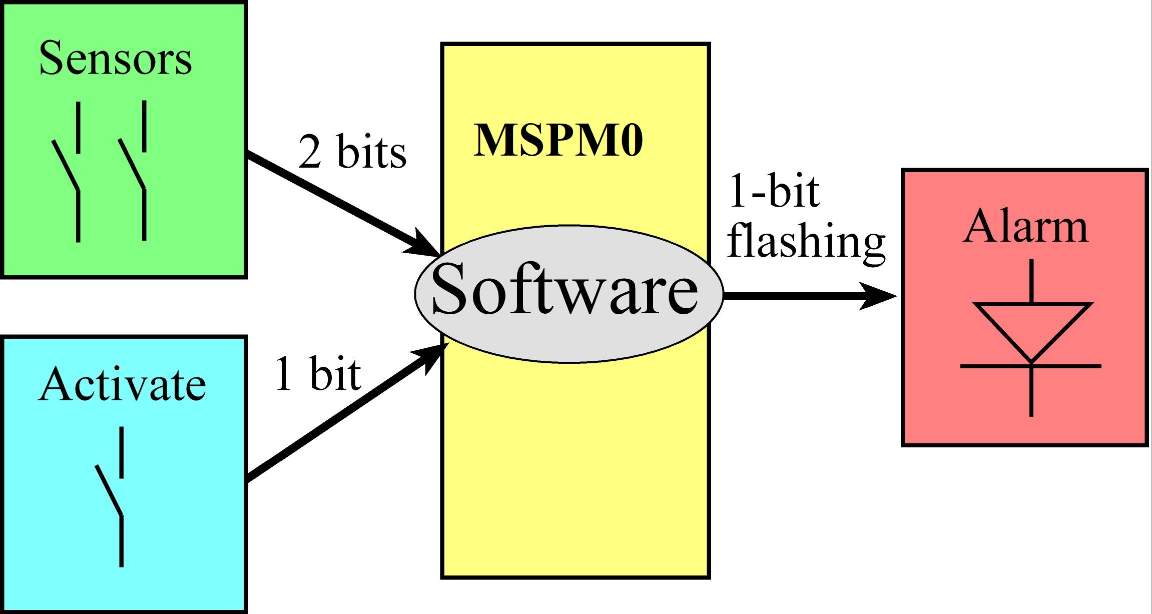
Figure 2.8.1. Data Flow Graph for Security System
The data-flow diagram gives us a blueprint for both the hardware circuit we are going to build and the software we are going to write. Lets first build the circuit:

Figure 2.8.2. Hardware circuit
: Describe the similarities between a data flow graph and a hardware circuit.
2.8.4 Software Design
Programs themselves are written in a linear or one-dimensional fashion. In other words, we type one line of software after another in a sequential fashion. Writing programs this way is a natural process, because the computer itself usually executes the program in a top-to-bottom sequential fashion. This one-dimensional format is fine for simple programs, but conditional branching and function calls may create complex behaviors that are not easily observed in a linear fashion. Even the simple systems have multiple software tasks. Furthermore, a complex application will require multiple microcontrollers. Therefore, we need a multi-dimensional way to visualize software behavior. Flowcharts are one way to describe software in a two-dimensional format, specifically providing convenient mechanisms to visualize multi-tasking, branching, and function calls. Flowcharts are very useful in the initial design stage of a software system to define complex algorithms. As an added benefit, flowcharts can be used in the final documentation stage of a project in order to assist in its use or modification.
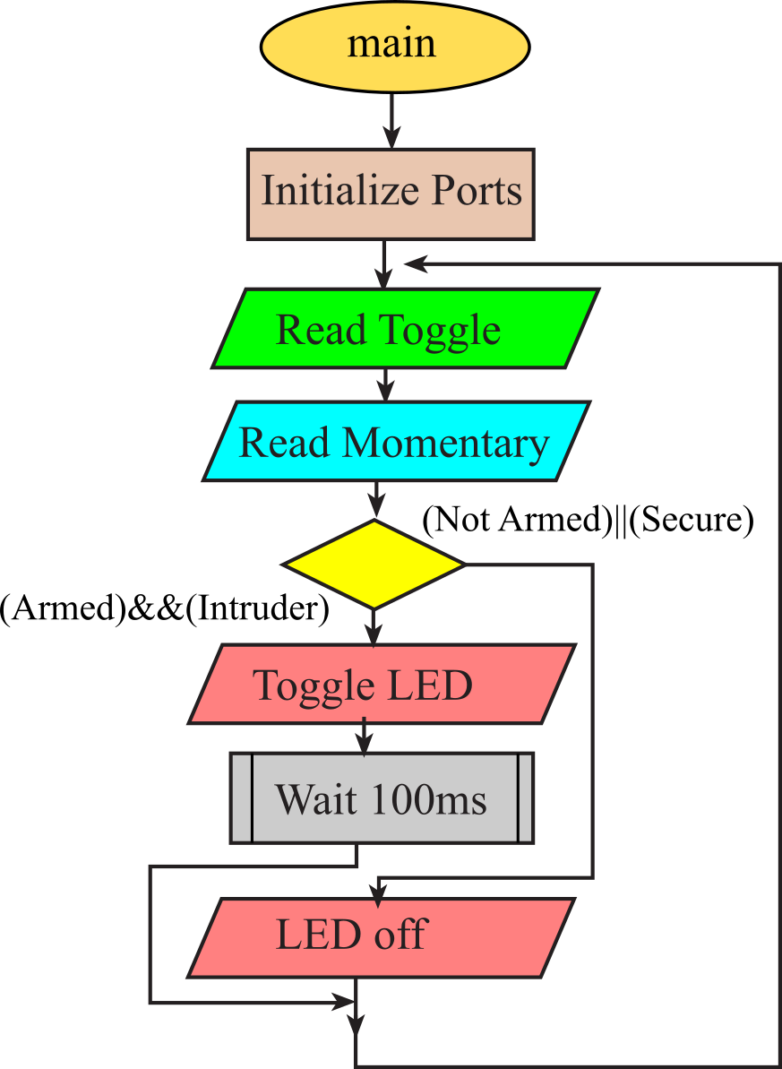
Figure 2.8.3. Flowchart for the Software
The code that implements the flowchart design described above is given below. This solution uses a friendly approach to accessing Port B. Which implies that we could use the other pins in Port B without changing this code.
|
Init: // PB4 output, PB2,PB1,PB0 input |
// PB4 output, PB2,PB1,PB0 input |
Program 2.8.1. Software system that flashes the LED
if it is armed and if there is an intruder.
: Explain how the main program uses registers R0-R2 as compared to how is uses R4-R7.
: Why are the values in R4-R7 set once, before the loop?
2.8.5. Testing
Video 2.8.5. Testing the circuit
As a general practice embedded systems developers start with first testing their solutions in a simulated environment (if possible) before running it on the real board with real hardware. Note that, just because your testing proves successful in simulation it does not mean it will succeed on the real board. However, failure to run in simulation almost always guarantees that it will fail on the real board.
2.8.6 Conclusion
We have successfully designed, built and tested a Security system. As a last step, we'll look back at the requirements and see if we met the timing specifications. In particular, we will check to see if our calculations used for sizing the resistors in the switch and LED interfaces match actual observations.
2.9. Designing a NOT gate using a LaunchPad
In this section we will combine many of the concepts presented in this chapter to design, build and test a NOT gate using the MSPM0 microcontroller. Any two GPIO pins could have been used, but we chose PB0 as input and PB1 as output. The system will make the PB1 output the logic NOT of the input on PB0. We will test the NOT gate by using a switch on PB0 to generate an input signal, and use an LED on PB1 to visualize the output. Basically if we press the switch, the input on PB0 will be high. The system will make the output on PB1 low, and the LED will be off. Conversely, if we release the switch, the input on PB0 will be low. The system will make the output on PB1 high, and the LED will be on. Figure 2.9.1 shows the data flow graph and Figure 2.9.2 shows the circuit used to test the not gate.
Video 2.9.1 Designing a Not gate ***needs recording

Figure 2.9.1. Data flow graph for the NOT gate.
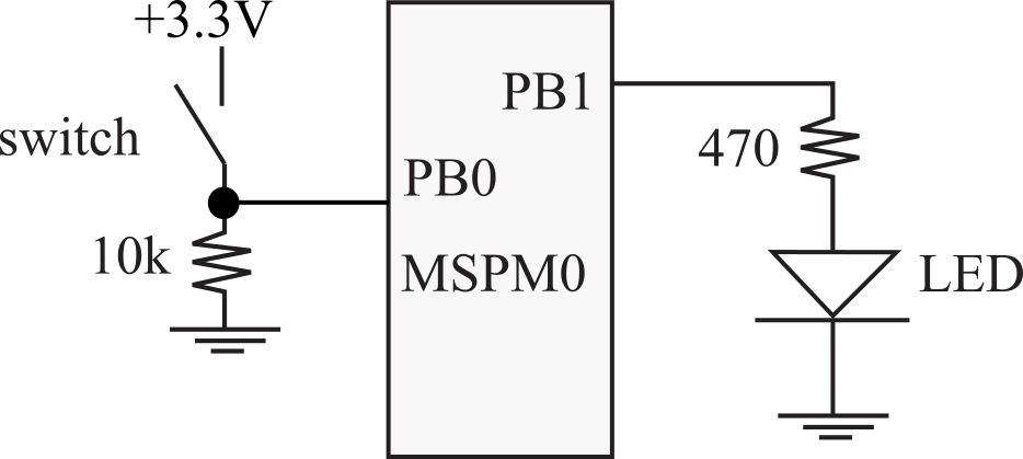
Figure 2.9.2. Circuit to test NOT gate.
To use GPIO pins we must first initialize the port. The pseudo code in Program 2.9.1 describes the NOT gate software. The initialization occurs once at the start, setting the two IOMUX registers and bit 1 of the DOE register. To read the state of the input, we read all the bits from DIN and use the AND operation to select just bit 0. We toggle the input data to implement the NOT operation and shift the result into position of bit 1. The shifting is required because the output pin exists in bit 1 position. The affect a change in just one output pin we: a) read all bits; b) clear the bit we wish to change; c) combine the 31 existing bits with the one new bit; and d) write the entire 32-bit value back to DOUT.
Video 2.9.2 Flow chart and Pseudo code ***needs recording
1) Initialize input pin and output pin
Set IOMUXPB1 to 0x00000081
Set IOMUXPB0 to 0x00040081
Set bit 1 in DOE
2) Read input from switch
Read all of DIN
Select just bit 0
3) Output = NOT(input)
Toggle just bit 0
Move bit 0 into bit 1
a) Read all of DOUT
b) Clear existing bit 1
c) Combine existing bits with new bit 1
d) Write to DOUT
4) Repeat steps 2,3 over and over
Program 2.9.1. Pseudo code for NOT gate.
Video 2.9.3 Morph pseudo code to assembly, reverse type into CCS ***needs recordingThe software shown in Program 2.9.2 implements the above pseudo code.
|
Init: |
void Init(void){ |
Program 2.9.1. NOT gate with PB1 as the output and PB0 as the input.
To test the system, we connect the switch to PB0 and LED to PB1, and single step through the code. We step through the loop with the switch not pressed to see the LED come on, and with the switch pressed to see the LED go off. If we connect a logic analyzer to PB1 and PB0, we test dynamic behavior of the system.
Video 2.9.4 Debug in CCS, debug with voltmeter and two-channel scope ***needs recording: Why is 0x81 stored into IOMUXPB1?
: Why is 0x00040081 stored into IOMUXPB0?
: Why do we set bit 1 of GPIOB_DOE31_0?
: Within the loop, what is the purpose of the ANDS instruction?
: Within the loop, what is the purpose of the EORS instruction?
: Within the loop, what is the purpose of the LSLS instruction?
: Within the loop, what is the purpose of the BICS instruction?
: Within the loop, what is the purpose of the ORRS instruction?
: In Program 2.9.2 runs, we defined a function Init, even though it was called only once. Would it have been better to embed the code directly into the main program eliminating the function call/return?
: In Program 2.9.2, consider registers R1, R2, R3 inside the loop. Perform an equivalence mapping from these three registers to the local variables in, out, and data in the C code.
Quiz 2.9
2.10. On Reset
Most microcontrollers have a button called the Reset
button. The Reset button on the MSPM0G3507 is labeled RESET (S3) and
located on the same side as the USB connector. Pressing the Reset
button triggers the Reset Procedure.
The reset procedure also executes when power is supplied to the the
microcontroller, in other words when the USB connector is connected to a power
source. The reset procedure involves 3 steps:
- The Stack Pointer, SP (R13) is initialized at reset to the 32-bit value stored at memory address 0x00000000. This location for the MSPM0G3507 holds the value 0x20208000, which is the address of the bottom of the RAM (0x20200000+32KiB = 0x20208000). This gives the stack maximum room to grow when data are pushed on it.
- The Program Counter, PC (R15) is initialized at reset to the 32-bit value stored at memory address 0x00000004 (called the Reset Vector). This location corresponds to the begining of the Interrupt Vector Table which holds addresses of Interrupt Service Routines that we want to execute when corresponding interrupts occur. The Reset Button triggers one such interrupt, i.e., the Reset Interrupt. The address stored there is the address of the "Reset Handler".
- The Link Register (R14) is initialized at reset to 0xFFFFFFFF, an initial value of no particular significance.
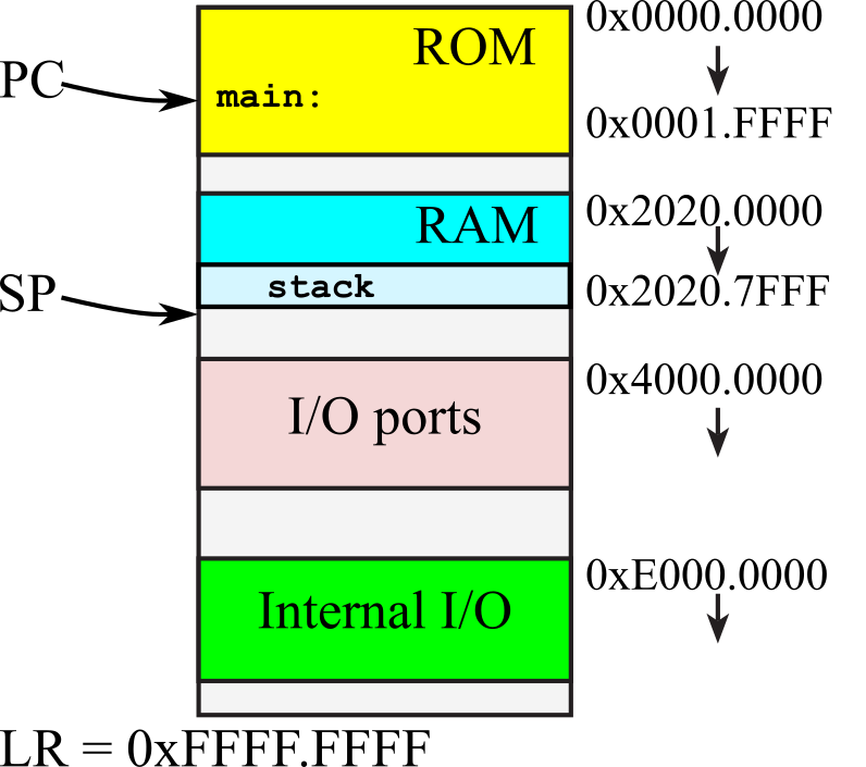
Figure 2.10.1. Initial values on reset, PC points to main, SP points to the bottom of the stack and LR is 0xFFFFFFF.
Note that at the end of the Reset Procedure, the PC points at the Reset
Handler and the code present there executes. This code calls an
initialization routine which eventually calls the main subroutine that is the entry point of an assembly/C program. The initilization routine when the entry point is the main in a C program, initilizes global variables and then calls main. In assembly it simply calls main.
: On reset where does our software begin execution?
: Notice the initial SP is 0x20208000, which does not point to RAM. Why?
2.11. Lab 2 Hardware Interfacing LED, Switch
The details of the lab 2 can be found in GoogleDocs:
Lab 2. Hardware Interfacing of LED, Switch
This material was created to teach ECE319K at the University of Texas at Austin
Reprinted with approval from Introduction to Embedded Systems Using the MSPM0+, ISBN: 979-8852536594

Embedded
Systems - Shape the World by Jonathan Valvano and Ramesh Yerraballi is
licensed under a Creative
Commons
Attribution-NonCommercial-NoDerivatives 4.0 International License.
Based on a work at http://users.ece.utexas.edu/~valvano/mspm0/