
Chapter
3: Introduction to Interfacing
Jonathan Valvano and Ramesh Yerraballi
What makes this course so much fun is you will make your microcontroller interact with real physical devices. Input/output devices are critical components of an embedded system. In this chapter, you will learn how to connect switches and LEDs to the microcontroller. You will use switches to input data and use LEDs to output results. The switch, LED, and LaunchPad components will then be combined to create a system. To interface the switches and LEDs, you will need a solid understanding of Ohm's Law. If you may need to review current, voltage, power, and resistance, please see Appendix: Electronics.
Table of Contents:
Video 3.0. Circuit elements and Interfacing them to a Microcontroller
Reference material relative to this chapter:
As our software becoming more complex, we will need
to create functions. The SP points to data on the top of the stack.
We use push to save data and pop to retrieve data. The stack operates in a
last in first out manner. Let's present rules for using the stack
1. Functions should have an equal number of
pushes and pops
2. Stack accesses should not be performed
outside the allocated area
3. Stack reads and writes should not be
performed within the free area
4. Stack push should first decrement SP,
then store the data
5. Stack pop should first read the data,
and then increment
The stack grows downwards in memory as we push data on to it so, although
we refer to the most recent item as the “top of the stack” it
is actually the item stored at the lowest address! To push data
on the stack, the stack pointer is first decremented by 4, and then the
32-bit information is stored at the address specified by SP. To pop data
from the stack, the 32-bit information pointed to by SP is first
retrieved, and then the stack pointer is incremented by 4. SP points to
the last item pushed, which will also be the next item to be popped. The
boxes in Figure 3.1 represent 32-bit storage elements in RAM. The grey
boxes in the figure refer to actual data stored on the stack, and the
white boxes refer to locations in the stack area, but do not contain stack
data. This figure illustrates how the stack is used to push the contents
of Registers R0, R1, and R2 in that order. Assume Register R0 initially
contains the value 1, R1 contains 2, and R2 contains 3. The drawing on the
left shows the initial stack. The software executes these six instructions
in this order:
PUSH {R0}
PUSH {R1}
PUSH {R2}
POP {R3}
POP {R4}
POP {R5}

Figure 3.1. Stack picture showing three numbers first being pushed, then three numbers being popped. You are allowed to draw stack pictures so that the lowest address is on the top (like this one) or so that lowest address is on the bottom. It is important however to be clear, accurate, and consistent.
Remember the order in the register list does not matter. The register with the lower number is stored in memory with the lower address. These are the same instructions
PUSH {R2,R5}
PUSH {R5,R2}
We use the BL instruction to call a
subroutine. The BL instruction will save the return address in LR
and branch to the subroutine. The BX LR will return
the LR back into the PC, causing control flow to revert
back to the place from which the function was called. If one function
calls another it will need to save the LR on the stack. In
general we will adhere to the following rules according to ARM
Architecture Procedure Call Standard (AAPCS)
We use R0,R1,R2,R3 as input
parameters
We use R0 as the return parameter.
We can freely use R0,R1,R2,R3,R12 without
needing to push or pop.
We can use R4-R11, but must push the
values at the start and pop the values at then end.
Time is one of the most important aspects of an embedded system. Throughout the course we will develop more complex, but more accurate methods for the software to control when events occur. We will begin with the most simple, a software delay loop. When performing Labs 3 and 4 with software delay loops, you will witness this method is inaccurate and hard to manage. Therefore for Labs 3 and 4 we expect the timing to be approximate. Lab 5 will introduce a hardware timer, and Lab 6 will introduce interrupts. Program 3.1 shows one possible way to create a software delay loop. The NOP instructions are added to increase the value of the time delay. To determine the actual delay you will have to run this code on your microcontroller and measure the delay with a scope or logic analyzer. This delay function is 100ns*count. The ALIGN 8 pseudo-op fixes a time of 3 bus cycles to execute the BNE instruction regardless of the machine code alignment.
;
Input: R0 is count, the amount to delay in 100ns
ALIGN 8
Delay NOP ;dummy operation
NOP
NOP
NOP
SUBS R0,R0,#1
BNE Delay
BX LR
Program 3.1. Software delay loop.
One of the ways we affect execution flow is the conditional. In the last chapter, we presented if-then, while-loop, and do-while in C. Here, we present a simple approach to create conditionals in assembly. To compare two values, they must be the same type.
First, we present an approach to conditionally test for individual bits.
Let mask specify which bit to test. For example, to test bit 3, we set the mask to 0x08.
In general the mask for bit n is 1<<n.
The approach is
Bring the entire value into R0
Check for bit n using ANDS R0,R0,#mask
Execute one of the following conditionals
BEQ target ; Branch if R0 bit n is 0
BNE target ; Branch if R0 bit n is 1
For example, let's write software that sets bit 1 of variable V1 to 1 if bit 8 of variable V0 is set. The flowchart is given the following figure. Notice, we skip over the body if bit 8 is clear.
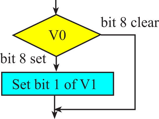
For the assembly implementation, we assume variable V0 is in register R0 and V1 is in register R1. The mask for bit 8 is 0x0100. The assembly version destroys R12.
|
ANDS R12,R0,#0x0100 BEQ next ORR R1,R1,#0x02 ; set bit 1 next |
if((V0&0x0100) == 0x0100{ V1 |= 0x02; } |
Program 3.2. Conditional to test individual bits.
Next, we
present if-then for signed 32-bit integers. The approach is
Bring the first value into R0
Bring the second value into R1
Compare the two values using CMP R0,R1
Execute one of the following signed conditionals
BEQ target ; Branch if R0 equals R1
BNE target ; Branch if R0 does not
equal R1
BLT target ; Branch if R0 is less than
R1 (signed)
BLE target ; Branch if R0 is less than
or equal to R1 (signed)
BGE target ; Branch if R0 is greater
than or equal to R1 (signed)
BGT target ; Branch if R0 is greater
than R1 (signed)
The approach is similar when comparing two unsigned
32-bit integers
Bring the first value into R0
Bring the second value into R1
Compare the two values using CMP R0,R1
Execute one of the following unsigned
conditionals
BEQ target ; Branch if R0 equals R1
BNE target ; Branch if R0 does not
equal R1
BLO target ; Branch if R0 is less than
R1 (unsigned)
BLS target ; Branch if R0 is less than
or equal to R1 (unsigned)
BHS target ; Branch if R0 is greater
than or equal to R1 (unsigned)
BHI target ; Branch if R0 is greater
than R1 (unsigned)
Examples of conditional operations were presented back in
Section 2.6.
The LaunchPad evaluation board (Figure 3.2) is a low-cost development board available as part number EK-TM4C123GXL. The microcontroller board provides an integrated In-Circuit Debug Interface (ICDI), which allows programming and debugging of the onboard TM4C123 microcontroller. One USB cable is used by the debugger (ICDI), and the other USB allows the user to develop USB applications (device). The user can select board power to come from either the debugger (ICDI) or the USB device (device) by setting the Power selection switch.
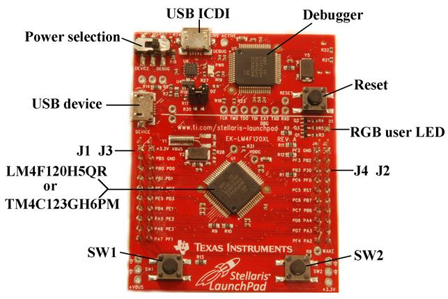
Figure 3.2. Tiva LaunchPad based on the TM4C123GH6PM.
Pins PA1 – PA0 create a serial port, which is linked through the debugger cable to the PC. The serial link is a physical UART as seen by the TM4C and mapped to a virtual COM port on the PC. The USB device interface uses PD4 and PD5. The JTAG debugger requires pins PC3 – PC0. The LaunchPad connects PB6 to PD0, and PB7 to PD1. If you wish to use both PB6 and PD0 you will need to remove the R9 resistor. Similarly, to use both PB7 and PD1 remove the R10 resistor.
The Tiva LaunchPad evaluation board has two switches and one 3-color LED. See Figure 3.3. The switches are negative logic and will require activation of the internal pull-up resistors. In particular, you will set bits 0 and 4 in GPIO_PORTF_PUR_R register. The LED interfaces on PF3 – PF1 are positive logic. To use the LED, make the PF3 – PF1 pins an output. To activate the red color, output a one to PF1. The blue color is on PF2, and the green color is controlled by PF3. The 0-Ω resistors (R1, R2, R11, R12, R13, R25, and R29) can be removed to disconnect the corresponding pin from the external hardware.
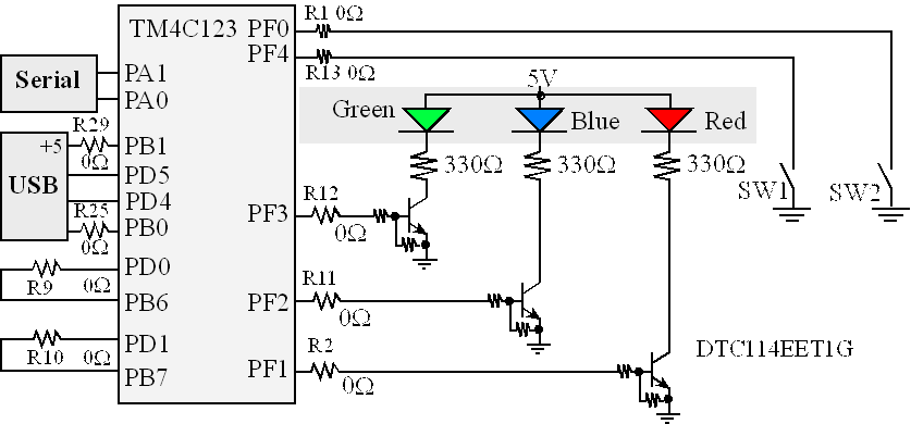
Figure 3.3. Switch and LED interfaces on the Tiva LaunchPad Evaluation Board. The zero ohm resistors can be removed so the corresponding pin can be used for its regular purpose.
The following tool allows
you to test your understanding of what happens when you WRITE to the DATA
register for PortF.
Note, writing to input pins has no effect. See what happens if you click
on one of the two switches.
Video 3.2. Device registers, Port Initialization steps with an PortF as an example
In most cases, a software module needs access to only some of the port pins. If two or more software modules access the same port, a conflict will occur if one module changes modes or output values set by another module. It is good software design to write friendly software, which only affects the individual pins as needed. Friendly software does not change the other bits in a shared register. Conversely, unfriendly software modifies more bits of a register than it needs to. The difficulty of unfriendly code is each module will run properly when tested by itself, but weird bugs result when two or more modules are combined.
Consider the problem that a software module needs to output to just Port A bit 7. After enabling the clock for Port A, we use read-modify-write software to initialize just pin 7. The following initialization does not modify the configurations for the other 7 bits in Port A. Unlocking is not required for PA7 (just PD7 and PF0 require unlocking)
SYSCTL_RCGCGPIO_R |= 0x00000001; // activate clock for Port A
delay = SYSCTL_RCGCGPIO_R; // allow time for clock to start
GPIO_PORTA_DIR_R |= 0x80; // PA7 outGPIO_PORTA_DEN_R |= 0x80; // enable digital I/O on PA7
There is no conflict if two or more modules enable the clock for Port A. The best way for microcontrollers to access individual port bit is to use read-modify-write software to change just one pin. A read-or-write sequence can be used to set bits.
|
LDR R1, =GPIO_PORTA_DATA_R LDR R0, [R1] ; previous ORR R0, R0, #0x80 ; set bit 1 STR R0, [R1] |
// make PA7 high GPIO_PORTA_DATA_R |= 0x80; |
A read-and-write sequence can be used to clear one or more bits.
|
LDR R1, =GPIO_PORTA_DATA_R LDR R0, [R1] ; previous BIC R0, R0, #0x80 ; clear bit 1 STR R0, [R1] |
// make PA7 low GPIO_PORTA_DATA_R &= ~0x80; |
Video 3.3. Software Development of solution
Video 3.4. Writing friendly code
To build circuits, we’ll use a solderless breadboard, also referred to as a protoboard. The holes in the protoboard are internally connected in a systematic manner, as shown in Figure 3.4. The long rows of holes along the outer sides of the protoboard are electrically connected. Some protoboards like the one in Figure 3.4 have four long rows (two on each side), while others have just two long rows (one on each side). We refer to the long rows as power buses. If your protoboard has long rows on the side, we will connect one long row to +3.3V and another long row to ground. In the middle of the protoboard, you’ll find two groups of holes placed in a 0.1 inch grid. Each adjacent row of five pins is electrically connected. We insert components like resistors, switches and LEDs into these holes. If integrated circuits (IC) are to be placed on the protoboard, it is done such that the two rows of pins straddle the center valley.
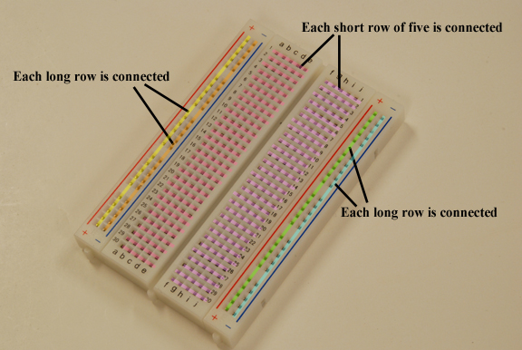
Figure 3.4. The pins on each of the four long rows are connected. The 5 pins in each short row are connected. Place a +3.3V wire from the Launchpad to one long row. Place a ground wire from the LaunchPad to another long row.
To build a circuit and to connect the circuit to the microcontroller we will use 22-gauge or 24-gauge solid wires. We strip off about 1/4 to 1/2 inch of insulation so the bare wire can be pushed straight into a hole. We only push one wire into a hole keeping track of which rows are internally connected.
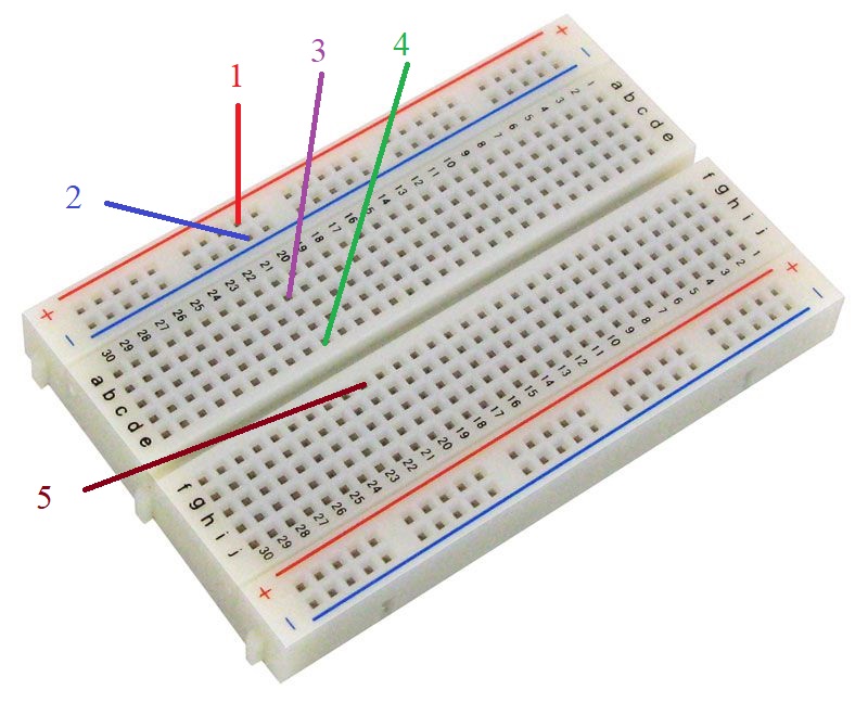
: In the above figure, the five colored lines represent wires plugged into the protoboard. All five wires are plugged into row 21. Which wires are connected via the protoboard?
Before interfacing switches, let's review how an input port converts voltage into digital logic. Most pins on the TM4C microcontrollers are 5V-tolerant, meaning an input voltage from 2.145 to 5.0 V will be considered high, and a voltage from 0 to 1.155 V will be considered as low. Since the microcontroller is built with CMOS logic we assume the current into the input port is 0.
The first input device we will interface is the switch. It allows the human to input binary information into the computer. Typically we define the asserted state, or logic true, when the switch is pressed. Contact switches can also be used in machines to detect mechanical contact (e.g., two parts touching, paper present in the printer, window open/closed, or wheels on the ground etc.) A single pole single throw (SPST) switch has two connections as shown in Figure 3.5. In a normally open switch (NO), the resistance between the connections is infinite (over 100 MΩ on the B3F tactile switch) if the switch is not pressed, and the resistance is zero (under 0.1 Ω on the B3F tactile switch) if the switch is pressed.
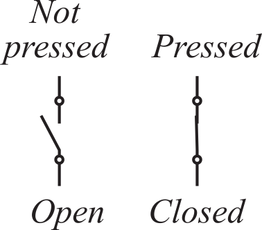
Figure 3.5. Single Pole Single Throw (SPST) Switch interface. When not pressed, the switch is open (over 100MΩ). When pressed, the switch is closed (under 0.1Ω).
We encourage you to read the data sheet for your switch and find which pins connect to the switch. Data sheet for the B3F-1059
Video 3.5. B3F Switch Datasheet
To convert the 100MΩ/0.1Ω resistance into a digital signal, we can use a pull-down resistor to ground or a pull-up resistor to +3.3V as shown in Figure 3.6. Notice that 10 kΩ is 100,000 times larger than the on-resistance of the switch and 10,000 times smaller than its off-resistance. Another way to choose the pull-down or pull-up resistor is to consider the input current of the microcontroller input pin. The current into the microcontroller will be less than 2µA (shown as IIL and IIH in the data sheet). So, if the current into microcontroller is 2µA, then the voltage drop across the 10 kΩ resistor will be 0.02 V, which is negligibly small. With a pull-down resistor shown on the right side of Figure 3.6, the digital signal will be low if the switch is not pressed and high if the switch is pressed. The signal being 3.3V when the switch is pressed is defined as positive logic, because the asserted switch state is a logic high. Conversely, with a pull-up resistor shown on the left side of Figure 3.6, the digital signal will be high if the switch is not pressed and low if the switch is pressed. The signal being 0V when the switch is pressed is defined as negative logic, because the asserted switch state is a logic low.

Figure 3.6. Two ways to interface a Single Pole Single Throw (SPST) Switch to the microcontroller.
: On the left side of Figure 3.6, when the switch is pressed, will the signal s be a logic 0 or logic 1?
: On the right side of Figure 3.6, when the switch is pressed, will the signal t be a logic 0 or logic 1?
Video 3.6. Circuit for Switch Interface
To interface a switch we connect it to a pin, and we initialize the pin as an input. Figure 3.7 connects the switch to PA5, but any microcontroller pin could have been used.
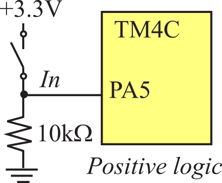
Figure 3.7. Interface of a switch to a microcomputer input.
Figure 3.8 shows how we could build this circuit with a protoboard and a LaunchPad. The brown-black-orange resistor is 10kΩ. The B3F switch should plug directly into the protoboard. The actual switch is across the pins that are closer to each other. The pins that are farther from each other will fit across the gap in the middle of the protoboard. It doesn't matter what color the wires are, but in this figure the wires are black, red and green. The two black wires are ground, the two red wires are +3.3V, and the green wire is the signal in, which connects the switch to pin PA5 of the microcontroller.
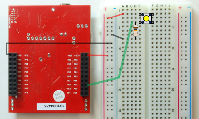
Figure 3.8. Construction of the interface of a B3F switch to a microcomputer input.
: Notice the switch in Figure 3.8 has four connections to the breadboard, but the switch in Figure 3.7 circuit only has two connections. What are the two extra connections on the actual switch?
The initialization function will set the direction register to input and enable the pin. Notice the software is friendly because it just affects PA5 without affecting the other bits in Port A. The input function reads Port A and returns a true (0x20) if the switch is pressed and returns a false (0) if the switch is not pressed. The software in Program 3.3 is called a driver, and it includes an initialization, which is called once, and a second function that can be called to read the current state of the switch. Writing software this way is called an abstraction, because it separates what the switch does (Init and Input) from how it works (PortA, bit 5, and TM4C123). The input function reads the entire port and selects bit 5 using a logical AND.
; Assembly version
Switch_Init
LDR R0,=SYSCTL_RCGCGPIO_R
LDR R1,[R0]
ORR R1,R1,#0x01 ;activate clock for Port A
STR R1,[R0]
NOP ; allow time for clock to start
NOP ; allow time for clock to start
LDR R0,=GPIO_PORTA_DIR_R
LDR R1,[R0]
BIC R1,R1,#0x20 ;direction PA5 input
STR R1,[R0]
LDR R0,= GPIO_PORTA_DEN_R
LDR R1,[R0]
ORR R1,R1,#0x20 ;enable PA5 digital port
STR R1,[R0]
BX LR
Switch_Input
LDR
R1,=GPIO_PORTA_DATA_R
LDR R0,[R1]
AND R0,R0,#0x20 ; 0x20(pressed) or 0(not pressed)
BX LR
//
C version
void Switch_Init(void){ volatile uint32_t delay;
SYSCTL_RCGCGPIO_R |= 0x01; // activate clock for Port A
delay = SYSCTL_RCGCGPIO_R; // allow time for clock to start
GPIO_PORTA_DIR_R &= ~0x20; // direction PA5 input
GPIO_PORTA_DEN_R |= 0x20; // enable PA5 digital port
}
uint32_t Switch_Input(void){
return(GPIO_PORTA_DATA_R&0x20); // 0x20(pressed) or 0(not pressed)
}
Program 3.3. Software interface for a switch on PA5.
Maintenance Tip: When interacting with just some of the bits of an I/O register it is better to modify just the bits of interest, leaving the other bits unchanged. In this way, the action of one piece of software does not undo the action of another piece. Modifying just the bits of interest is called friendly.
Observation: One of the complicating issues with mechanical switches is they can bounce (oscillate on and off) when touched and when released. The contact bounce varies from switch to switch and from time to time, but usually bouncing is a transient event lasting less than 5 ms. We can eliminate the effect of bounce if we design software that waits at least 10 ms between times we read the switch values.
Before interfacing LEDs, let's review how an output port converts digital logic into voltage. Software can configure output pins to set IOH and IOL to 2mA, 4mA or 8mA. All ports have DR2R DR4R and DR8R registers, which software can use to select the maximum current on each output pin.
A light emitting diode (LED) emits light when an electric current passes through it. LEDs have polarity, meaning current must pass from anode to cathode to activate, see Figure 3.9. The anode is labelled a or + , and cathode is labelled k or -. The cathode is the short lead and there may be a slight flat spot on the body of round LEDs. Thus, the anode is the longer lead. The brightness of an LED depends on the applied electrical power (P=Vd*Id). Notice in the LED operating range of 5 to 40 mA, the voltage only changes from 1.8 to 2.2V. For this reason, we will establish the desired brightness by setting the LED current rather than trying to set the LED voltage.
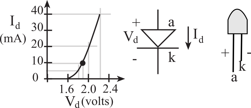
Figure 3.9. Positive logic LED interface (Lite-On LTL-10223W).
: Notice black dot in Figure 3.9 shows Vd=1.9V and Id=10mA for a power of 19mW. What would be the LED power if the LED voltage were to increase just a little bit toVd=2V?
We encourage you to open up the data sheet for your LED and find the curve similar to Figure 3.9. Data sheet for HLMP-4700. .
Video 3.8. Circuit for LED Interface
When the LED current is less than 8 mA, we can interface it directly to an output pin without using any integrated circuits. The LED shown in Figure 3.10a has an operating point of 1.6 V and 1 mA.

Figure 3.10. Interface of a low current LED
For the positive logic interface (Figure 3.10b) we calculate the resistor value based on the desired LED voltage and current
R = (VOH
- Vd) / Id =
(3.1 -
1.6) /0.001 =
1500Ω
where VOH is the output high voltage of the microcontroller output pin, which will be about 3.1V when sourcing 1mA of current. Since VOH can vary from 2.4 to 3.3 V, it makes sense to choose a resistor from a measured value of VOH, rather than the minimum value of 2.4 V. Negative logic means the LED is activated when the software outputs a zero. For the negative logic interface (Figure 3.10c) we use a similar equation to determine the resistor value
R = (3.3 - Vd
-
VOL ) / Id =
(3.3 - 1.6 - 0.2) /0.001 =
1500Ω
where VOL
is the output low voltage of the microcontroller output pin, which will be about
0.2V when sinking 1mA of current. Since VOL can
vary from 0 to 0.4 V, it makes sense to choose a resistor from a
measured value of VOL, rather than the maximum
value of 0.4 V.
Figure 3.11 shows how we could build this circuit with a protoboard and a LaunchPad. The brown-green-red resistor is 1.5kΩ. The LED should plug directly into the protoboard. The longer lead on the LED is the positive or anode. It doesn't matter what color the wires are, but in this figure the wires are black, red and green. The two black wires are ground, and the green wire is the signal out, which connects the switch to pin PA2 of the microcontroller.
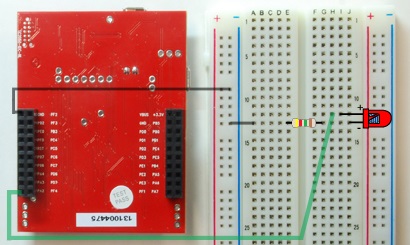
Figure 3.11. Construction of the interface of an LED to a microcomputer output.
: What resistor value in of Figure 3.10 is needed if the desired LED operating point is 1.8V and 5 mA? Use the positive logic interface and, VOH of 3.2V.
: What resistor value in of Figure 3.10 is needed if the desired LED operating point is 1.7V and 2 mA? Use the negative logic interface and, VOL of 0.2V.
The software in Program 3.4 is called a driver, and it includes an initialization, which is called once, and two functions that can be called to turn on and off the LED. Writing software this way is called an abstraction, because it separates what the LED does (Init, On, Off) from how it works (PortA, bit 2, TM4C123).
; Assembly version
LED_Init
LDR R0,=SYSCTL_RCGCGPIO_R
LDR R1,[R0]
ORR R1,R1,#0x01 ;activate clock for Port A
STR R1,[R0]
NOP
NOP ; allow time for clock to start
LDR R0,=GPIO_PORTA_DIR_R
LDR R1,[R0]
ORR R1,R1,#0x04 ;direction PA2 output
STR R1,[R0]
LDR R0,= GPIO_PORTA_DEN_R
LDR R1,[R0]
ORR R1,R1,#0x04 ;enable PA2 digital port
STR R1,[R0]
BX LR
LED_On
LDR R1,=GPIO_PORTA_DATA_R
LDR R0,[R1]
ORR R0,R0,#0x04 ; bit 2 high
STR R0,[R1]
BX LR
LED_Off
LDR R1,=GPIO_PORTA_DATA_R
LDR R0,[R1]
BIC R0,R0,#0x04 ; bit 2 low
STR R0,[R1]
BX LR
// C version
void LED_Init(void){ volatile uint32_t delay;
SYSCTL_RCGCGPIO_R |=
0x01; // activate clock for
Port A
delay =
SYSCTL_RCGCGPIO_R; // allow
time for clock to start
GPIO_PORTA_DIR_R |=
0x04; // set direction
to output
GPIO_PORTA_DEN_R |=
0x04; // enable
digital port
}
// Make PA2 high
void LED_On(void){
GPIO_PORTA_DATA_R |= 0x04;
}
// Make PA2 low
void LED_Off(void){
GPIO_PORTA_DATA_R &= ~0x04;
}
Program 3.4. Software interface for an LED on PA2
If the LED current is above 8 mA, we cannot connect it directly to the microcontroller because the high currents may damage the chip. There are many possible solutions to interface an LED needing more than 8 mA of current. Examples include 7405, 7406 or PN2222. We have chosen the ULN2003B because it has 7 drivers in each package. The ULN2003B comes in a DIP package with 7 base (B) signals, 7 collector (C) signals and one emitter (E) pin. Figure 3.12 shows one driver in the ULN2003B.The B signals are the inputs, the C signals are the outputs, and the E pin will be grounded. If the base input is high, the collector output will be low (0.5V). If the base input is low, the collector output will float (neither high nor low).
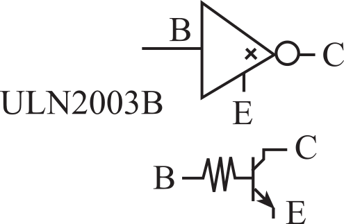
Figure 3.12. The ULN2003B LED driver.
For high current LEDs we typically use the 5V supply
rather than the 3.3V, because the available current at 5V is often much
more than the available current at 3.3V. Figure 3.13 shows how to
interface a 10 mA 1.9V LED using the ULN2003B. When the software writes a
logic 1 to the output port, the input to the ULN2003B becomes high, output
from the ULN2003B becomes low, 10 mA travels through the LED, and the LED
is on. When the software writes a logic 0 to the output port, the input to
the ULN2003B becomes low, output from the ULN2003B floats (neither high
nor low), no current travels through the LED, and the LED is dark.
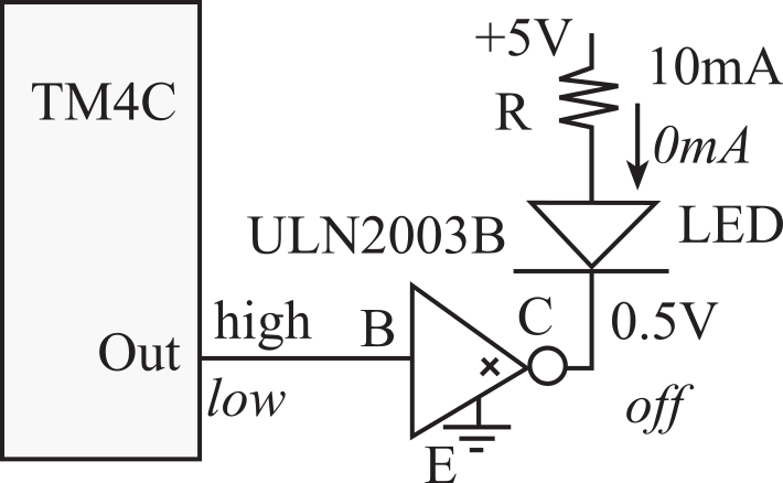
Figure 3.13. Interface a high current LED using a ULN2003B driver.
The value of the resistor is selected to establish the proper LED current. When active, the LED voltage will be between 1.8 and 2.2 V, and the power delivered to the LED will be controlled by its current. If the desired brightness requires an operating point of 1.9 V at 10 mA, then the resistor value should be
R = (5 - Vd - VCE) / Id = (5 - 1.9- 0.5) /0.01 = 260Ω
where Vd, Id is the desired LED operating point, and VCE is the output low voltage of the LED driver. If we use a standard resistor value of 270Ω in place of the 260Ω, then the current will be (5-1.9-0.5V)/270Ω, which is about 9.6 mA. This slightly lower current is usually acceptable.
: What resistor value in Figure 3.13 is needed if the desired LED operating point is Vd=1.7V and Id=11 mA?
Controlling time is an important function of an
embedded system. One of the methods software can perform to set the
delivered power to an external device is pulse width modulation
(PWM). The basic idea is to oscillate an output so fast the external
device does not respond to the individual on and off events. Rather, the
delivered power will be a function of the average, called duty cycle.
Let H be the time the output is high, and L the time the output is low.
For PWM we will set P=H+L as a constant, and adjust H and L. The duty
cycle is defined as
Duty Cycle = H/(H+L)
The human eye can see a flashing LED up to about 10
Hz. If we flash the LED at 100 Hz, our eyes will see a constant light, but
the brightness of the LED will depend linearly on the duty cycle. In
particular if the LED operating point is Vd, Id,
the LED power will be
Power = Vd*Id*H/(H+L)
Program 3.5 presents a simple PWM output. Notice that
this implementation uses all the processor time.
; R4 is H, the time the LED is on
; R5 is L, the time the LED is off (H+L should be constant)
PWM BL LED_On
MOV R0,R4 ;H
BL Delay
BL LED_Off
MOV R0,R5 ;L
BL Delay
B PWM
Program 3.5. Software implementation of PWM.
: If H+L=100000, creating a 100 Hz wave in Program 3.5, how many different duty cycles can be created? How bits of precision does this represent?
Some problems are so unique that they require the engineer to invent completely original solutions. Most of the time, however, the engineer can solve even complex problems by building the system from components that already exist. Creativity will still be required in selecting the proper components, making small changes in their behavior (tweaking), arranging them in an effective and efficient manner, and then verifying the system satisfies both the requirements and constraints. When young engineers begin their first job, they are sometimes surprised to see that education does not stop with college graduation, but rather is a life-long activity. In fact, it is the educational goal of all engineers to continue to learn both processes (rules about how to solve problems) and products (hardware and software components). As the engineer becomes more experienced, he or she has a larger toolbox from which processes and components can be selected.
The hardest step for most new engineers is the first one: where to begin? We begin by analyzing the problem to create a set of specifications and constraints in the form of a requirements document. Next, we look for components, in the form of previously debugged solutions, which are similar to our needs. Often during the design process, additional questions or concerns arise. We at that point consult with our clients to clarify the problem. Next we rewrite the requirements document and get it reapproved by the clients.
It is often difficult to distinguish whether a parameter is a specification or a constraint. In actuality, when designing a system it often doesn’t matter into which category a parameter falls, because the system must satisfy all specifications and constraints. Nevertheless, when documenting the device it is better to categorize parameters properly. Specifications generally define in a quantitative manner the overall system objectives as given to us by our customers.
Constraints, on the other hand, generally define the boundary space within which we must search for a solution to the problem. If we must use a particular component, it is often considered a constraint. In this class, we constrain most designs to include a Tiva LaunchPad. Constraints also are often defined as an inequality, such as the cost must be less than $50, or the battery must last for at least one week. Specifications on the other hand are often defined as a quantitative number, and the system satisfies the requirement if the system operates within a specified tolerance of that parameter. Tolerance can be defined as a percentage error or as a range with minimum and maximum values.
In engineering everything is either a system or an interface between systems. For example a switch can be considered a system. When we interface it to the LaunchPad the switch-LaunchPad combination is a new system. Therefore, we begin by collecting the components required to build the system. We then combine the components and debug the system. As the components are combined we create new more powerful components. When writing software, we can use flowcharts to develop new algorithms. The more we can simulate the system, the more design possibilities we can evaluate, and the quicker we can make changes. Debugging involves both making sure it works, together with satisfying all requirements and constraints.
First, lets develop a requirements document. The main purpose of a requirements document is to serve as an agreement between you and your clients describing what the system will do. This agreement can become a legally binding contract. Write the document so that it is easy to read and understand by others. It should be unambiguous, complete, verifiable, and modifiable.
The requirements document should not include how the system will be designed. This allows the engineer to make choices during the design to minimize cost and maximize performance. Rather it should describe the problem being solved and what the system actually does. It can include some constraints placed on the development process. Ideally, it is co-written by both the engineers and the non-technical clients. However, it is imperative that both the engineers and the clients understand and agree on the specifics in the document.
Video 3.9. Requirments Document
Before we get into the actual design of the Security system, lets take stock of the components we will use in building the prototype.
A data flow graph is a block diagram of the system, showing the flow of information. Arrows point from source to destination. Notice that a data flow graph looks like a block diagram of the system. In fact we draw a data flow graph by showing how the components are connected together. By visualizing the flow of data we are able to identify the components of the system and the nature of the data they work with.
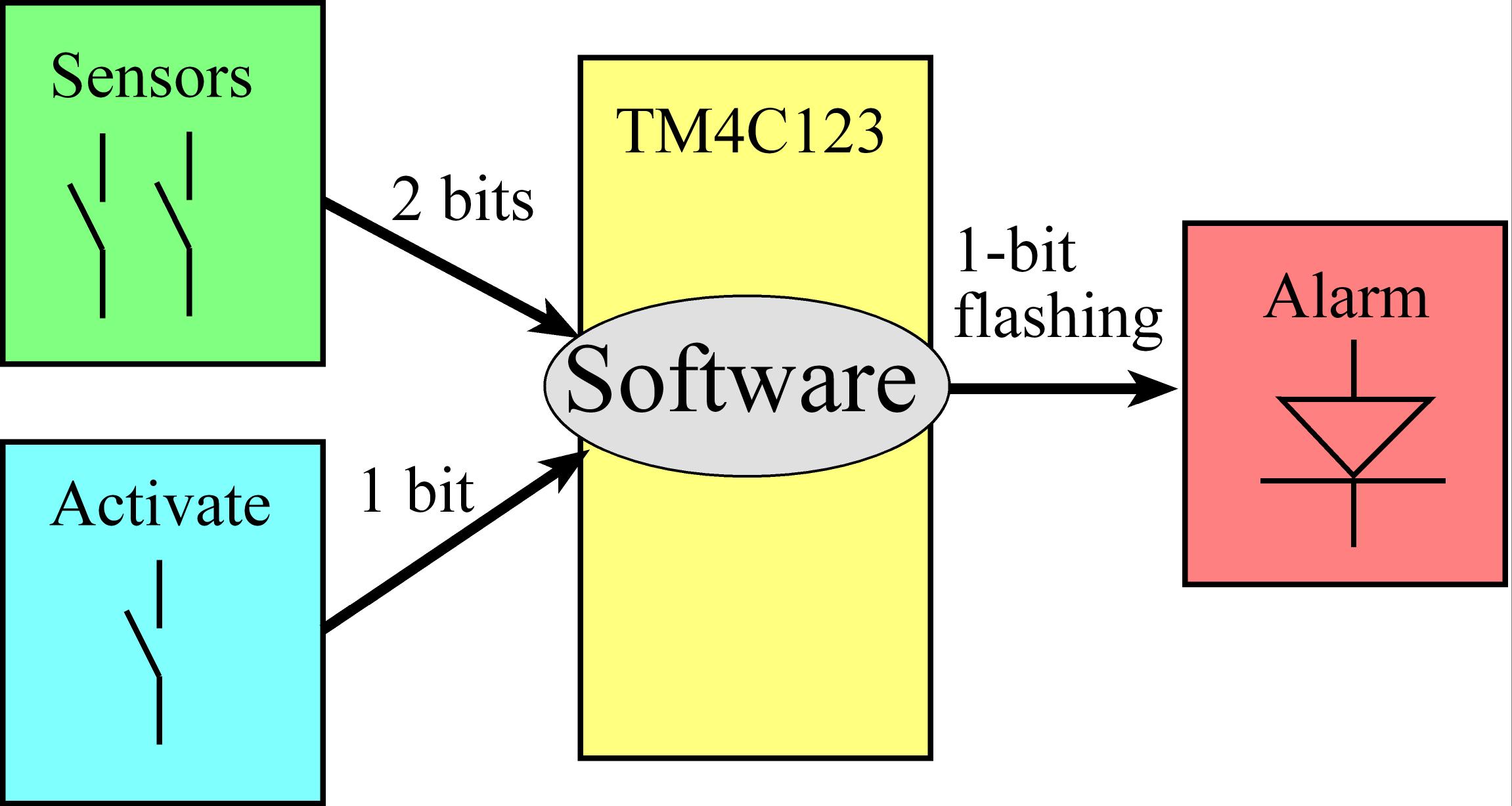
Figure 3.14. Data Flow Graph for Security System
The data-flow diagram gives us a blueprint for both the hardware circuit we are going to build and the software we are going to write. Lets first build the circuit:
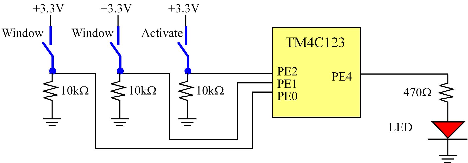
Figure 3.15. Hardware circuit
Video 3.12. Building the circuit
Programs themselves are written in a linear or one-dimensional fashion. In other words, we type one line of software after another in a sequential fashion. Writing programs this way is a natural process, because the computer itself usually executes the program in a top-to-bottom sequential fashion. This one-dimensional format is fine for simple programs, but conditional branching and function calls may create complex behaviors that are not easily observed in a linear fashion. Even the simple systems have multiple software tasks. Furthermore, a complex application will require multiple microcontrollers. Therefore, we need a multi-dimensional way to visualize software behavior. Flowcharts are one way to describe software in a two-dimensional format, specifically providing convenient mechanisms to visualize multi-tasking, branching, and function calls. Flowcharts are very useful in the initial design stage of a software system to define complex algorithms. As an added benefit, flowcharts can be used in the final documentation stage of a project in order to assist in its use or modification.
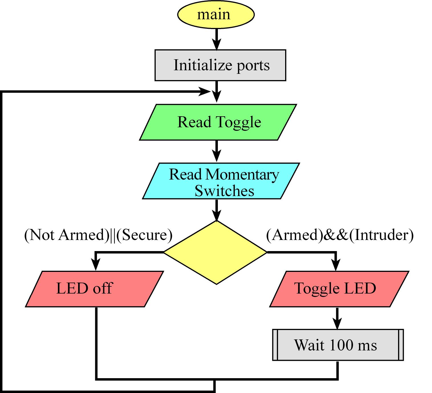
Figure 3.16. Flowchart for the Software
The code that implements the flowchart design described above is given below. This solution uses a friendly approach to accessing Port E. Which implies that we could use the other pins in Port E without changing this code.
void
delayms(uint32_t
ms);
void EnableInterrupts(void);
int main(void){ uint32_t volatile delay;
uint32_t
arm,sensor;
TExaS_Init(); // activate multimeter, 80 MHz
SYSCTL_RCGCGPIO_R |=
0x10; // Port E clock
delay =
SYSCTL_RCGCGPIO_R; // wait
3-5 bus cycles
GPIO_PORTE_DIR_R |=
0x10; // PE4 output
GPIO_PORTE_DIR_R &=
~0x07; // PE2,1,0 input
GPIO_PORTE_DEN_R |=
0x17; // enable
PE4,PE2,PE1,PE0
EnableInterrupts();
while(1){
arm = GPIO_PORTE_DATA_R&0x04;
// arm 0 if deactivated, 1 if activated
sensor = GPIO_PORTE_DATA_R&0x03; // 1 means ok,
0 means break in
if((arm==0x04)&&(sensor != 0x03)){
GPIO_PORTE_DATA_R ^= 0x10;
// toggle output for alarm
delayms(100); // 100ms delay
makes a 5Hz period
}else{
GPIO_PORTE_DATA_R &=
~0x10; // LED off if deactivated
}
}
}
Program 3.6. Software system that flashes the LED
if it is armed and if there is an intruder.
As a general practice embedded systems developers start with first testing their solutions in a simulated environment (if possible) before running it on the real board with real hardware. Note that, just because your testing proves successful in simulation it does not mean it will succeed on the real board. However, failure to run in simulation almost always guarantees that it will fail on the real board.
Video 3.14. Testing in Simulation
Video 3.15. Testing the Prototype
We have successfully designed, built and tested a Security system. As a last step, we'll look back at the requirements and see if we met the timing specifications. In particular, we will check to see if our calculations used for sizing the resistors in the switch and LED interfaces match actual observations.
Reprinted with approval from Introduction to Embedded Systems, 2022, ISBN: 978-1537105727
